Atomic structure of the single step and dynamics of Sn adatoms on the SiSn surface
Abstract
The atomic structure of well-ordered single steps on the SiSn surface and the dynamics of Sn adatoms in the vicinity of these steps were studied. The work was performed using low temperature scanning tunneling microscopy (LT-STM) and ab initio calculations based on the density functional theory. The STM tip was used to record the tunneling current versus time on top of oscillating adatoms, keeping the feedback loop turned off. The dynamics of adatoms, detected as the telegraph noise present in the tunneling current, was registered near the steps at 80 K. The atomic structure model of the single steps consisting of Sn atomic chains along the steps was developed. This structure leads to the formation of potential double-wells near the steps acting as traps for Sn atoms and explains the fluctuating current recorded in these areas.
pacs:
68.35.Md, 68.43.Fg, 68.35.JaI INTRODUCTION
Among other chemical elements used in silicon-based heterostructures for micro- and photoelectronic applications, tin attracts particular interest since it belongs to the same group as silicon and germanium. Although the Si surface is a primary substrate for the fabrication of functional heterostructures based on GeSn solid solutions Wirths et al. (2016), Si substrates provide a higher hole mobility for GeSn MOSFETs Maeda et al. (2015). However, the epitaxial growth of high-quality GeSn alloys on the Si surface is still a challenge because of the Sn surface segregation and low solubility in the Ge matrix Wirths et al. (2016); Oehme et al. (2013). On the Si surface, GeSn structures without the Sn segregation are observed after the low-temperature growth of 5 nm amorphous GeSn layer Maeda et al. (2015) or after the initial Sn film growth followed by the Ge deposition and substrate annealing Yu et al. (2016). In the second case, the Sn film starting from an even submonolayer thickness acts as a surface active agent affecting the following epitaxial growth on the Si surface Dolbak and Olshanetsky (2008); Lin (1995); Iwanari and Takayanagi (1992); Iwanari et al. (1992). In particular, the surfactant Sn layer enhances the surface diffusion and suppresses the 2D island nucleation during the Ge/Si Dolbak and Olshanetsky (2008) and Si/Si Iwanari and Takayanagi (1992); Iwanari et al. (1992) epitaxy on the Si surface and prevents the Ge segregation in near-surface layers of the Si substrate Lin (1995). This modification of the atomic processes on the growing Si surface is related to the formation of Sn-induced surface reconstructions, different from the intrinsic dimer-adatom-stacking fault structure Takayanagi et al. (1985), which change the nature of the interaction between deposited atoms and the substrate. The presence of preliminarily formed Sn-induced reconstructions on the Si surface also changes the orientations of the epitaxial Sn layers growing at room temperatures Ryu et al. (2002). The investigation of the Sn/Si surface atomic structure forming at the initial stages of Sn film growth is a way to understand how to avoid the Sn segregation at the following stages of GeSn structure fabrication.
Depending on the substrate temperature and deposited coverage, the Sn adsorption on the Si(111)-7×7 surface induces the formation of the following ordered surface phases Charrier et al. (2001); Nogami et al. (1989); Törnevik et al. (1994): ( shortly), (mosaic phase) and . The structure, atomic and electronic properties of these reconstructions on the Si surface were well studied by the scanning tunneling microscopy (STM) technique Nogami et al. (1989); Törnevik et al. (1994, 1991); Eriksson et al. (2010); Levermann et al. (1996); Ichikawa and Cho (2003) and by ab initio calculations Ichikawa and Cho (2003); Ressel et al. (2004). To reveal the properties of a perfect reconstructed surface, these investigations were carried out mostly on singular regions far from surface defects and atomic steps always existing on real substrates. However, the kinetics of epitaxial growth and structural transitions on the Si surface is directly determined by the features of atomic processes near the steps Latyshev et al. (1992); Kato et al. (2000) depending on the step edge orientation Romanyuk et al. (2007); Voigtländer (2001); Teys et al. (2014); Rogilo et al. (2013). One interesting consequence of this is the reduced symmetry island growth on the higher symmetry substrate demonstrated in case of the Si and Ge epitaxy on the SiBi surface Romanyuk et al. (2007). In the present work, we used STM and ab initio calculations based on the density functional theory to reveal the atomic structure of the steps on the SiSn surface and to study the dynamics of adsorbed atoms in the vicinity of such steps.
The paper is organized as follows: after reviewing the experimental and calculation procedures, we report on the atomic structure model of the single step on the SiSn surface, give corresponding experimental and calculated STM images and show the localization of empty and filled electronic states near the steps. In Sec. 4.2 we first review the previous results related to the Sn adatom dynamics on the flat Sn surface regions of Si and Ge. Then we report the STM data related to the adatom dynamics on the stepped SiSn surface, calculate the potential energy surfaces (PES) for Sn and Si adatoms, compare the experimental and calculated data, and explain the fluctuating current detected near the steps.
II METHODS
II.1 Experimental procedure
The experiments were carried out using an ultra-high vacuum system (base pressure ) equipped with a low temperature scanning tunneling microscope (LT-STM, Omicron) and a low energy electron diffraction (LEED). Silicon substrates were cut from Si n-type wafers with resistivity . The sample preparation started from clean Si surfaces. The Si clean surface was prepared by the annealing at and flashing the sample at for about . The samples were resistively heated by a direct current. The surface reconstruction was confirmed by LEED and STM before the Sn evaporation. Sn was evaporated from a Knudsen effusion cell. The effusion cell was thoroughly outgassed before its use in order to maintain the pressure in the range during the metal deposition. The evaporation rate was measured by using the quartz crystal thickness monitor. A nominal monolayer Sn deposition was performed at room temperature, followed by the sample annealing at . After that the formation of the Sn reconstruction was confirmed by LEED and STM. Electrochemically etched tungsten STM tips were used after a cleaning procedure by electron bombardment. The reported STM images were recorded at 80 K in the constant-current mode. The STM scanner was calibrated by using the Si surface as a reference.
Tunneling current vs time traces (“current traces” hereafter) were acquired concomitantly to the acquisition of constant current STM images by interrupting the tip scan every five points and five lines over the chosen area. At every single grid point, the STM feedback loop was switched off and the tunneling current was recorded with a sampling rate of . In this way, we could observe steps in the current trace if an adatom underneath the STM tip is unstable, i.e. moves horizontally or vertically. Furthermore, it is possible to exactly locate the position of moving adatoms on the STM images. To show where such traces were recorded on the sample surface, we calculated the standard deviation () of all the current traces and reported these values on the z axis of a grid. The resulting images (hereinafter called “ maps”) show a brighter color for higher values, evidencing where the adatom movement occurs. It is important to emphasize that, with such an acquisition method, the uncertainties of the actual tip location during the current trace acquisition are greatly reduced because the STM image and the current traces are acquired concomitantly. The maximum limit of the detectable frequency in the current traces in our STM system is estimated to be , while the lower limit is about . The method was successfully applied to the study of Sn atom dynamics on flat SiSn and GeSn surfaces at low temperatures Ronci et al. (2005, 2007) and was described in detail in Ref. Ronci et al., 2010.
II.2 Computational details
The calculations were carried out using the pseudopotential Troullier and Martins (1991) density functional theory siesta code Soler et al. (2002) within generalized gradient approximation (GGA) to the exchange and correlation interactions between electrons Perdew et al. (1996). We did not consider the corrections to GGA, which could help to better describe the electron correlation effects in the SiSn system. Such corrections, although having some influence on the calculated electronic structure Flores et al. (2001); Profeta and Tosatti (2007); Modesti et al. (2007); Schuwalow et al. (2010), are expected to have a small impact on the calculated total energies and forces, and the resulting atomic structure, studied in this work. The valence states were expressed as linear combinations of the Sankey-Niklewski-type numerical atomic orbitals Soler et al. (2002). In the present calculations, the polarized double- functions were assigned for all atom species. This means two sets of s- and p-orbitals plus one set of d-orbitals on silicon and tin atoms, and two sets of s-orbitals plus a set of p-orbitals on hydrogen atoms. The electron density and potential terms were calculated on a real space grid with the spacing equivalent to a plane-wave cut-off of 200 Ry.
In our calculations we used (111)-slabs with single steps in the step-down direction (-steps in short). The dangling bonds at the slabs bottom side were saturated by H atoms, while the top -terraces were constructed according to the Sn atomic model consisting of Sn-adatoms on -sites Nogami et al. (1989). The slab thickness was about Å (four Si-bilayers), and the Å thick vacuum layer was used. The positions of all slab atoms (except for the Si atoms in the bottom bilayer and all H atoms) were fully optimized until the atomic forces became less than eV/Å. Two different calculation cells were used in this work. For the calculation of relative formation energies and PES maps, we used slabs with lateral dimensions and a grid of -points in the Brillouin zone Monkhorst and Pack (1976). Larger slabs with lateral dimensions and a grid of -points were used for the calculation of STM images. Si and Sn chemical potentials were calculated using bulk unit cells and -point grids. The Sn chemical potential was calculated using the bulk -phase of Sn having the diamond structure and known as gray tin. The calculated Si and Sn bulk-lattice constants are and , which are close to experimental values and , respectively. The constant-current STM images were produced based on the Tersoff-Hamann approximation Tersoff and Hamann (1985) using the eigenvalues and eigenfunctions of the Kohn-Sham equation Kohn and Sham (1965) for a relaxed atomic structure. Experimental and calculated STM images were processed using the WSxM software Horcas et al. (2007).
In this work, we compared the relative formation energies of the stepped SiSn surface according to different atomic configurations of the step edge. The SiSn surface having an unreconstructed step edge (described in the text) after the structure relaxation was treated as a reference surface. The relative surface formation energies (per unit area) were calculated according to the procedure described in Ref. Battaglia et al., 2008:
| (1) |
where is the unit cell area of the slab in the xy plane, refers to the total energy of the reference slab containing the unreconstructed step after the structure relaxation, is the total energy of the slab according to the trial step model, and account for the number of Si and Sn atoms in the trial model in excess of those in the reference model.
and are the chemical potentials of Si and Sn, which are the energy per atom in the reservoirs with which the surface is assumed to be in equilibrium. Since the surface is in equilibrium with the bulk Si substrate, is the energy per atom in bulk Si. The adsorbate chemical potential was treated as a variable, since its exact value is unknown. It corresponds to a real physical variable that can be externally tuned Battaglia et al. (2008). Under thermodynamic equilibrium conditions the surface having the lowest formation energy will be realized. The change of leads to a change of surface formation energy, which may be followed by structural phase transitions. The chemical potential in bulk -phase Sn () may be considered as the upper bound for the Sn chemical potential. If , then bulk -phase Sn would be energetically more favorable than any adsorbed phase, which would lead to the precipitation of bulk Sn on the Si surface. In the opposite case of extreme low values, the clean Si surface with no Sn adatoms becomes the most stable. Thus, the low/high values should favor atomic structures with a low/high amount of Sn atoms on the Si surface, respectively. In this work we are interested in the intermediate values, when the Sn-Si compound surface phases are stable.
The PES maps describing the energetics of adatoms on the stepped SiSn surface were produced for the positions of the adsorbed probe Sn (Si) atom within a symmetry-irreducible half of the calculation cell. For each xy-coordinate, the adsorbed atom was initially placed approximately Å above the surface and its z-coordinate was allowed to relax, while the coordinates in the xy-plane were kept fixed. The positions of all remaining atoms, but the bottom Si-H units, were fully optimized until atomic forces became less than eV/Å. The total of 444 points forming a grid with about Å spacing were calculated in the calculation cell half. The PES data for the whole calculation cell were recovered by applying the mirror symmetry transformation to the calculated PES data. The exact energies of local energy minima on PES were calculated with a free-moving probe atom placed near the local energy minima.
III RESULTS AND DISCUSSION
III.1 Atomic structures of the single step on the SiSn surface
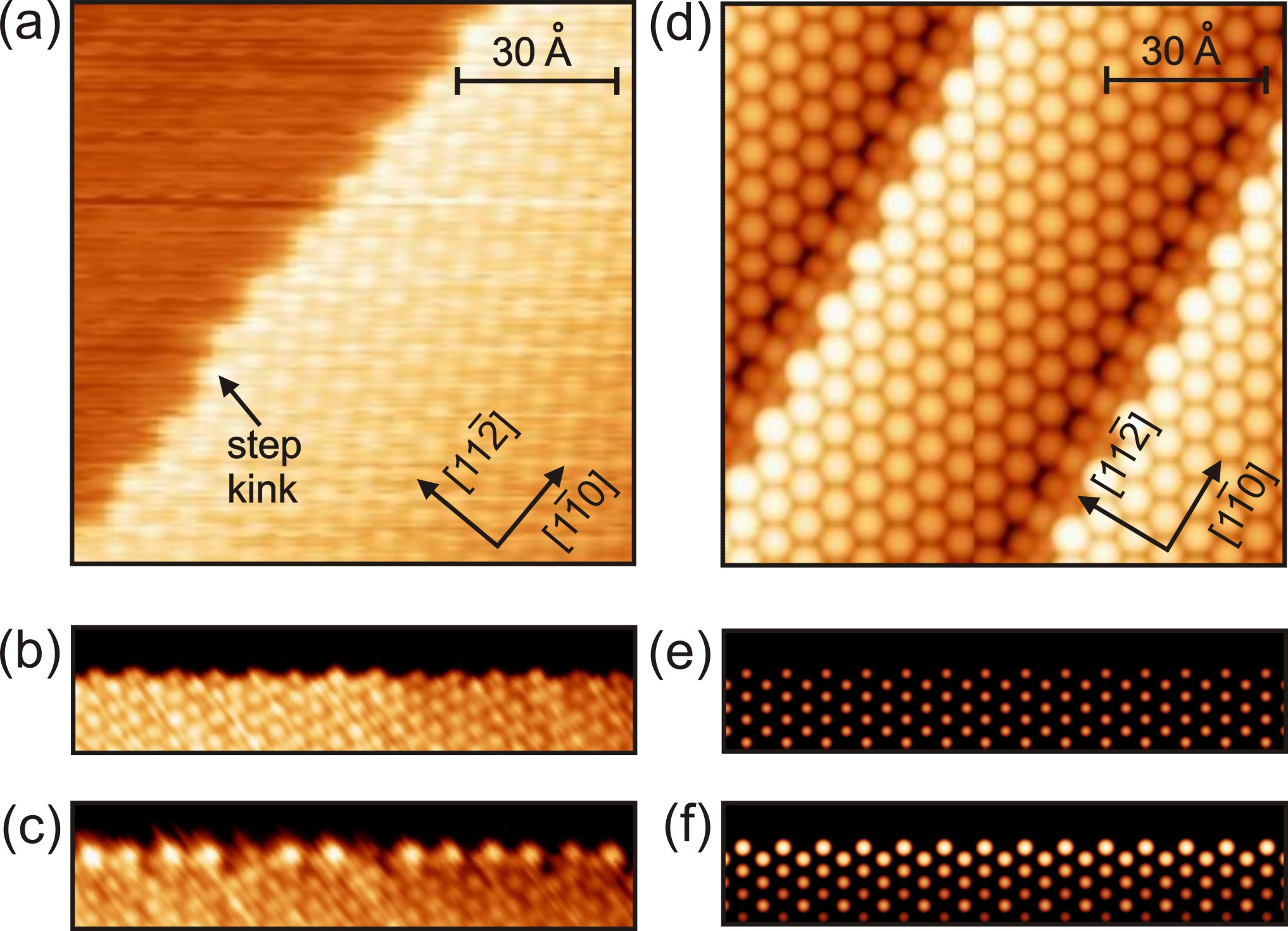
The starting point of our investigation of the step atomic structure is the information provided by STM images. In Fig. 1(a) is a typical STM-image of the atomic step found on the SiSn surface. Each bright spot in the STM image represents a Sn adatom. In Figs. 1(b) and 1(c) are the high-resolution STM-images of the step edge obtained at and , respectively. It is seen in Fig. 1(c) that the Sn adatoms at the upper terrace edge look brighter than those far from it at . Since this effect was observed only at a negative bias, then it is unlikely that it is a real topography feature. The effect is most probably due to a charge transfer and associated higher density of filled local electron states (electrons) at the Sn atoms located at the upper terrace edge.
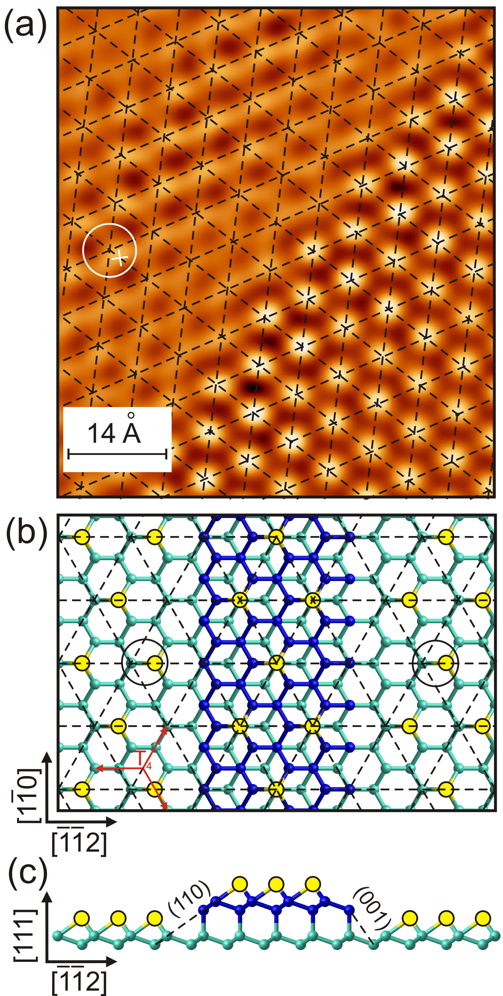
In Fig. 2(a) is the experimental STM image of the single step on the SiSn surface acquired at after a linear distortion correction and an FFT band pass filtering. The key for understanding the step edge directions is in the mutual alignment of the Sn lattices on the neighboring terraces separated by the single step. Accordingly, the hexagonal lattice was drawn across the Sn adatom positions on the upper terrace (lower right part of Fig. 2(a). It is clear that the Sn adatoms on the lower terrace (upper left part of Fig. 2(a)) are located on the same lines drawn perpendicular to the step edge as the Sn adatoms on the upper terrace. Two (the only possible) models of unreconstructed steps on the SiSn surface compatible with the above observation are shown in Figs. 2(b) and 2(c). Thus, the direction along the step edge in Figs. 1(a) and 2(a) is of -type, as it follows from the models shown in Figs. 2(b) and 2(c).
A more difficult question is the step-down direction in the experimental STM images shown in Figs. 1(a) and 2(a). This direction can be either , resulting in a step in which the bonds configuration is the same as on unreconstructed surface (right parts of Figs. 2(b) and 2(c)) or , in which the bonds configuration is as on the surface (left parts of Figs. 2(b) and 2(c)). It should be noted that these two directions are physically nonequivalent for crystals with a diamond lattice, i.e. they lead to a different step atomic structure with different properties. To solve this problem, we note that the bright spots (Sn atoms) on the lower terrace shown in Fig. 2(a) are shifted from the nearest nodes of the hexagonal lattice by about lattice period ( Å) towards the step edge. The shift is clearly visible near the central part of the lower terrace. The Sn atom positions on the lower terrace near the step edge should be ignored since, in this area, the image may be altered by an undesired tunneling through the side of the STM tip. The same shift direction can be observed only for steps. Therefore, the steps observed in our experimental STM images in Figs. 1(a) and 2(a) are steps.
The trial atomic models of the steps for ab initio calculations were constructed in accordance with the information provided by experimental STM images. In this work, we compare the stability of different step configurations by calculating the relative formation energies of regular stepped surfaces according to various step models. The step formation energies were not calculated explicitly.
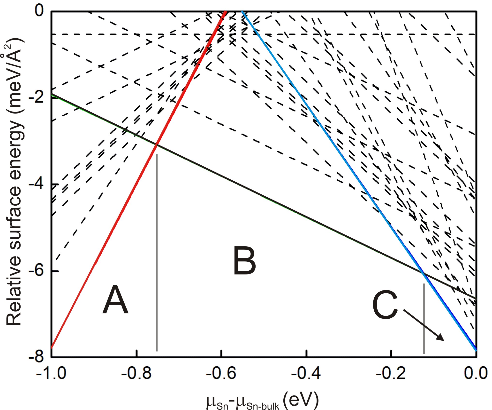
We performed an extensive search for the lowest energy atomic configuration of the stepped SiSn surface. 50 atomic models were evaluated, and our results are shown in Fig. 3. Three solid lines - red, black, and blue - represent the surface energy graphs for three lowest energy atomic configurations, A, B, and C, depending on the value, while the dashed lines in Fig. 3 are from other higher energy trial models.
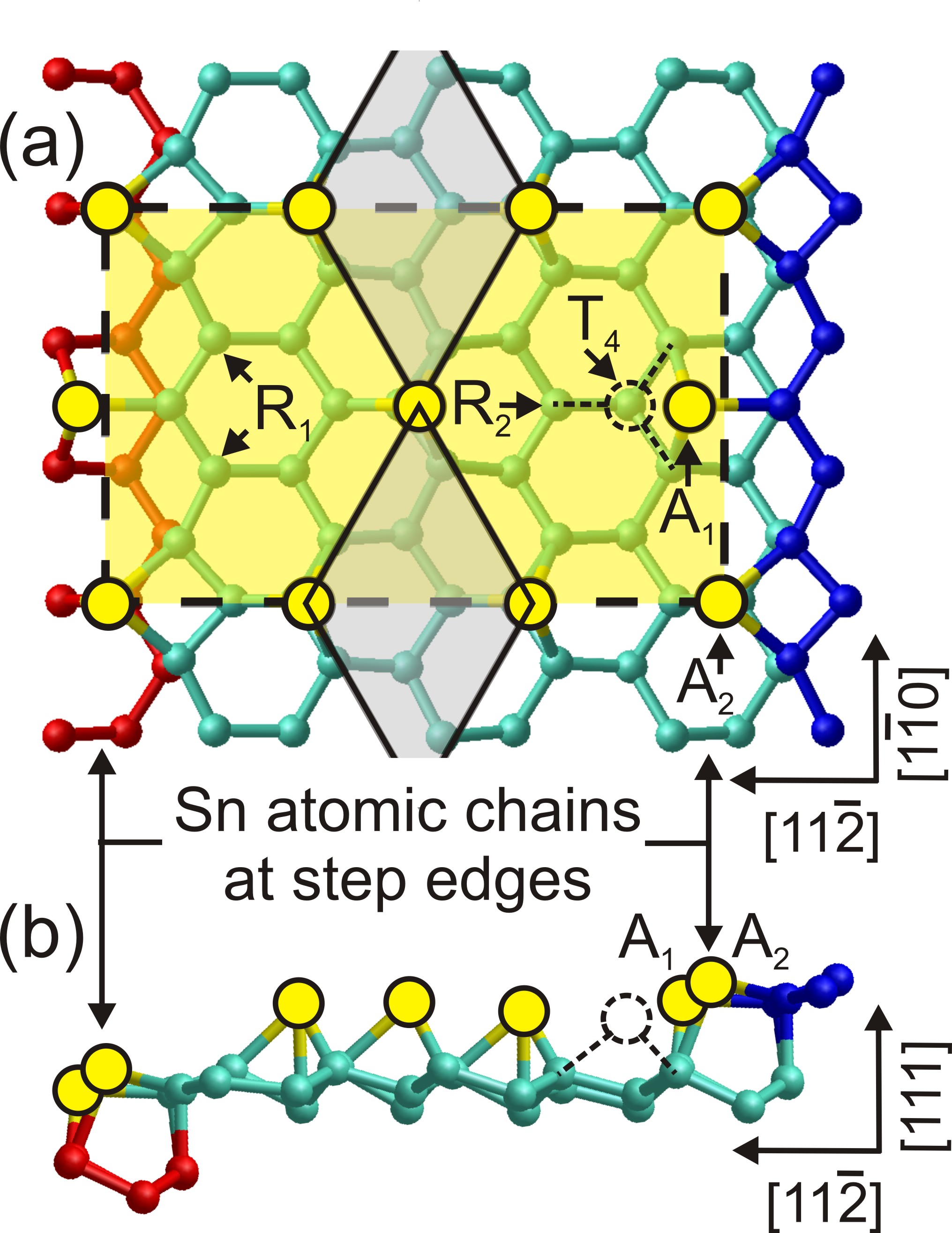
The atomic step model “B”, which is stable in a wide range of values (Fig. 3) is shown in Fig. 4. The difference between this model and the model of unreconstructed step shown in Figs. 2(b) and 2(c) (left parts of these figures) is the presence of Sn atomic chain consisting of and Sn adatoms decorating the step edge. The adatom can be considered as the one taken from the Sn structure on the lower terrace by shifting from the neighboring site to the step edge (see the dashed circle outlining the previous position of this adatom). The adatom is an additional Sn atom, not existing in the unreconstructed step model. The model “B” contains Si atoms with unsaturated dangling bonds (rest atoms): on the upper terrace and on the lower terrace. The rest atoms show the -like (planar) configuration of saturated bonds after the structure relaxation. While exists also in the unreconstructed step model, the emergence of is caused by the Sn atom shift leading to the formation of step edge atom. All other Si bonds in the model, except for the bonds on and atoms, are saturated. It is difficult to resolve ,, and atoms experimentally since Sn adatoms, in the vicinity of the upper terrace edge, strongly hinder their imaging. The possible reason of why Sn atoms prefer and positions at the step edges is the bigger size of Sn atoms, as compared to that of Si. As a result, Sn atoms better fit the positions with large distances to the closest neighbors, as it is the case for and .
Model “C” is stable at the excess of Sn on Si surface, just before precipitation of the bulk Sn (Fig. 3). The only difference between “B” and “C” models is that, in case of the “C” model, the Si rest atom is substituted with the Sn atom. Both models result in very similar calculated STM images. Model “A” is stable at low values and contains no Sn atoms at all. This clean Si surface model is basically the unreconstructed step edge model shown in Figs. 2(b) and 2(c) (left parts) where all Sn atoms on terraces are substituted by Si atoms. Thus, the terraces in model “A” are structurally similar to the mosaic Sn -phase observed after the partial self-cleaning of Si terraces at elevated temperatures Charrier et al. (2001); Törnevik et al. (1994). The models “A” and “C” determine the upper and lower stability boundaries of the “B” model, which is most likely to be relevant for the experimentally observed step structure.
In Fig. 1(d) is a large-scale calculated STM image of the SiSn surface based on the atomic step model “B” shown in Fig. 4. In Figs. 1(e) and 1(f) are the STM images of the step edges calculated for and , respectively. The latter two images exhibit the same features as the experimental STM images shown in Figs. 1(b) and 1(c): namely, the spots associated with Sn adatoms at the very edge of the upper terrace are brighter than other spots on the filled states STM images ( ). This effect was not observed at in agreement with the experimental data (Figs. 1(b) and 1(e)). Thus, the experimental and calculated STM images demonstrate a good match, which is a prerequisite for a correct atomic model. It should be noted that few other trial models exhibited the same effect of bright terrace edges as the model shown in Fig. 4, but these atomic configurations had significantly higher formation energies.
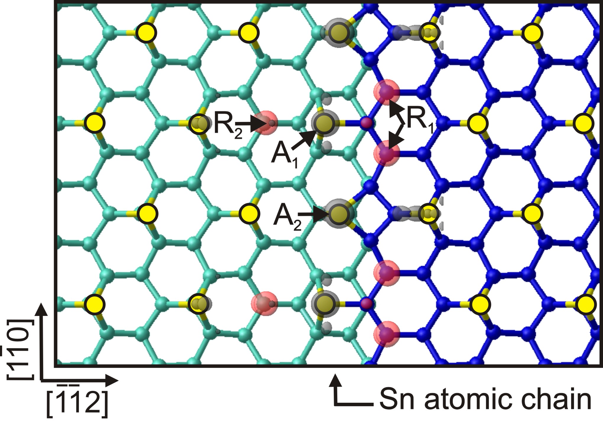
The charge distribution near the step edge is the reason for the increased intensity on Sn adatoms in the filled states experimental and calculated STM images. This effect was investigated in more detail. The calculated local density of states (LDOS) isosurfaces integrated in a 1.0 eV energy window below and above the calculated Fermi level are shown in Fig. 5. The atomic model superimposed on this pattern allows identifying the atoms acting as electron donors or acceptors. It is clear that the empty states are mostly concentrated on the Si rest atoms, while filled states are mostly located on and atoms of the Sn chain. Few filled states are also found on the Sn atoms near the lower and upper terrace edges.
III.2 PES and dynamics of Sn adatoms on the SiSn surface with steps
The dynamical fluctuations of Sn atoms on flat Sn/Si and Sn/Ge surfaces were studied in detail in Refs. Ronci et al., 2005 and Ronci et al., 2007 by recording the tunneling current as a function of time. Vertical fluctuations of Sn atoms within the surface reconstruction are related to the phase transition during the temperature decrease. The process is well described within the dynamical fluctuations model, at least in case of the Sn/Ge system. According to this model, the static structure is unstable and transforms into the structure with the Sn adatoms buckled up and down Avila et al. (1999). The observation of the structure, according to this theory, is due to the time averaged vertical fluctuations of Sn atoms, which is Å between the up-and-down positions on Sn/Ge Gori et al. (2009). The fluctuations were observed at in the Sn/Ge system and at in the Sn/Si system. While the stable structure was actually observed in the Sn/Ge system at , the reconstruction on Sn/Si persists even at a very low temperature, down to Ronci et al. (2010). The reason for that is a very low energy barrier ( Ronci et al. (2007)) associated with the phase transition on Sn/Si, which is much lower than that on Sn/Ge ( Ronci et al. (2005)). This results in the notable quantum tunneling of Sn adatoms between two stable positions on Sn/Si and that destroys the structural order Ronci et al. (2007).
Due to the very low energy barrier in the Sn/Si system, the frequency of Sn dynamical fluctuations at is expected to be well above the maximum limit of detectable frequency in our STM measurements (about ). It is possible to estimate how high the energy barriers have to be in order to observe the dynamical fluctuations in STM. To this end, we make use of the frequency () of thermally activated dynamical fluctuations using an Arrhenius relation , where , , and stand for the Boltzmann constant, sample temperature and attempt frequency, respectively, which can be approximated by the Debye frequency of Si (). Thus, for the upper limit of detectable frequency (), we get and for the lower limit () - .
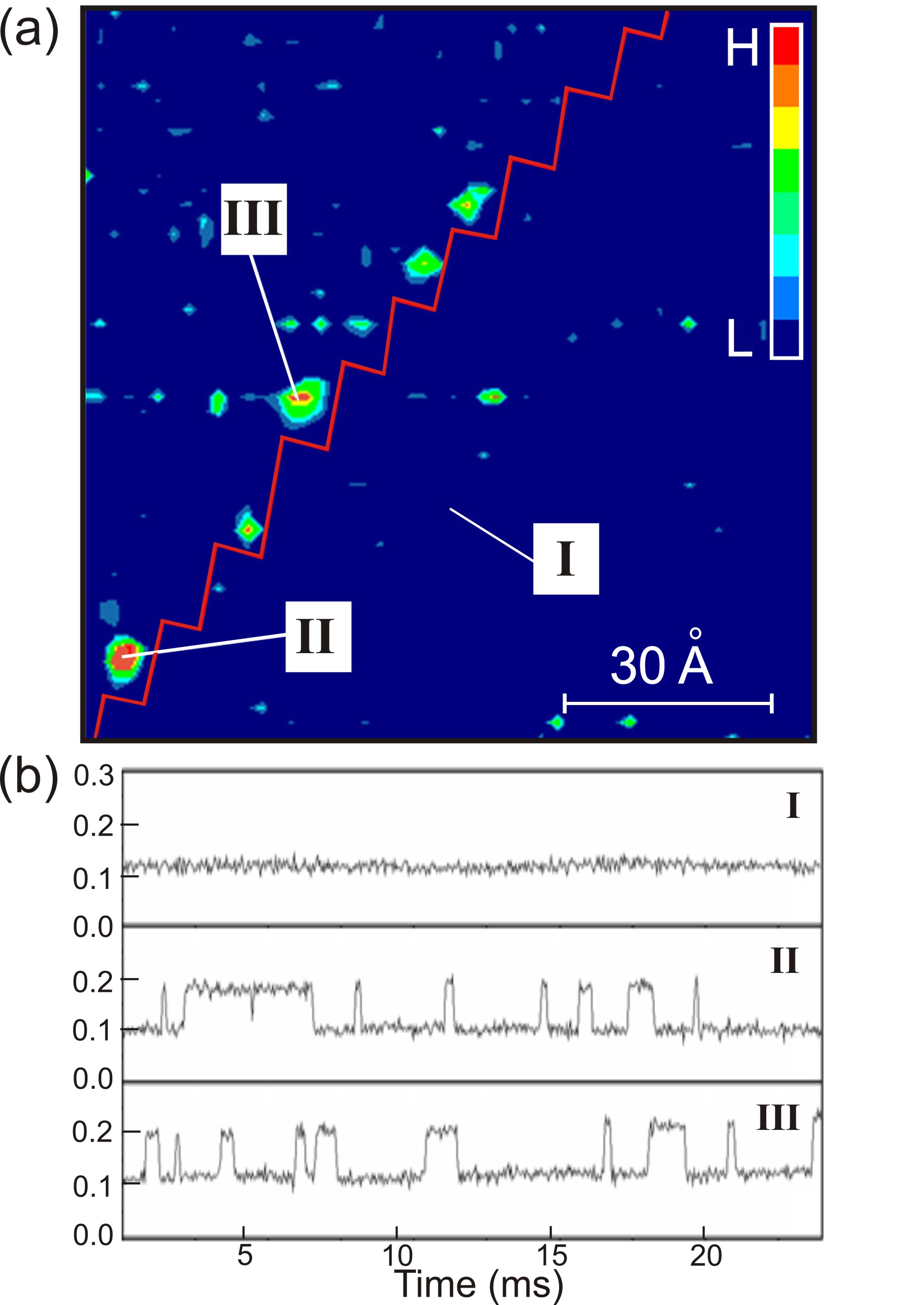
Figure 6(a) shows the map acquired concomitantly with the STM image shown in 1(a). All the current traces recorded on the terrace show a flat profile () consistent with the expected high frequency of Sn dynamical fluctuations at 80 K (see the current trace collected at point I, for example). However, the map clearly exhibits bright spots at the lower side of step edge, that show the presence of current traces with a high standard deviation value. As an example, two stepped current traces collected at points II and III are reported in Fig. 6(b). The observation of stepped current traces near the step edge at indicates that the energy barrier for the fluctuating adatoms in that area is much larger than that on the flat Sn/Si surface. It is also worth noting that, in spite of a very regular step structure visible in the STM image in Fig. 1(a), only a few irregular spots are visible in the map in Fig. 6(a). The reason for that will be clear from the results presented below.
The calculated PES for a Sn probe atom on the stepped SiSn surface with the atomic model “B” overlaid is shown in Fig. 7. Bright regions correspond to the energy minima, while dark regions indicate energy maxima. It is clear that the Sn adatom positions on the surface are the highest energy maxima on PES. This is because these atoms have only one dangling bond and, therefore, these sites are not favorable for the adsorption of additional probe Sn atom having four valence electrons. The positions of rest atoms also show energy maxima, but their values are lower than those found on Sn atoms.
| N | Relative energy (eV) | |
|---|---|---|
| Sn | Si | |
| 1 | 0 | 0 |
| 2 | -0.33 | -0.48 |
| 3 | -0.58 | -0.55 |
| 4 | -0.28 | -0.61 |
| 5 | -0.19 | -0.51 |
| 6 | -0.07 | -0.23 |
| 7 | -0.37 | -0.52 |
| 8 | -0.49 | -0.68 |
| 9 | -0.39 | -0.47 |
| 10 | -0.18 | -0.23 |
All Si bonds on the SiSn surface are saturated by Sn atoms making this surface inert. Thus, according to Fig. 7, each Sn half unit cell shows only a single shallow local minimum on site (minimum ). The energy of this local minimum is taken as the energy zero in our calculations. The energies calculated for different energy minima on PES for Sn and Si probe atoms are shown in Tab. 1. As expected, the deepest minima are located near the step edge since this area contains many unsaturated bonds. According to Fig. 7, each rest atom is surrounded by four local minima on PES: , 2, 3, 3 for and , 8, 9, 10 for . The region between and adatoms contains three additional minima: , 5, 6. The location of the deep local minima around rest atoms and near adatoms is typical of the surfaces containing these atoms, and it was also observed in other systems Chang and Wei (2003); Zhachuk et al. (2010). The reason for this is that the adsorbed atom in the vicinity of rest atoms and adatoms may effectively saturate several bonds. According to Tab. 1, the two neighboring minima near labeled on PES are the deepest (global) minima for the probe Sn atom on the stepped SiSn surface. Therefore, these minima should be the preferential adsorption sites for Sn atoms at a low sample temperature.
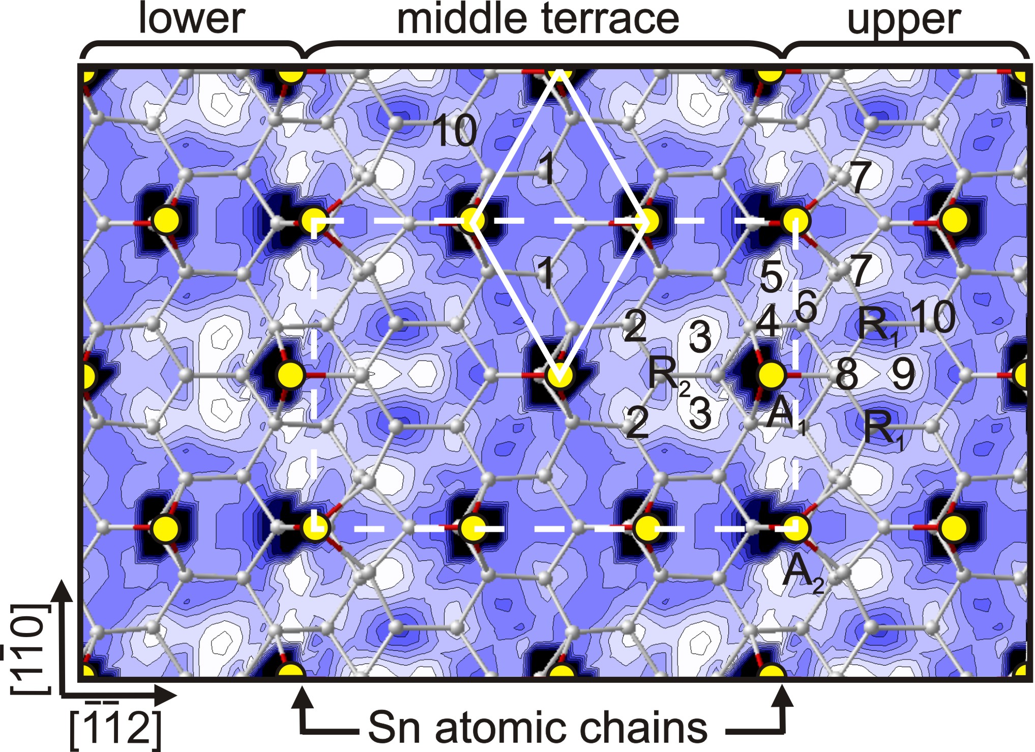
The calculated PES (Fig. 7) shows that the energy barrier between two neighboring sites is among the lowest on the surface. As it follows from the symmetry of the computational cell, the saddle point between these two sites is situated in the plane crossing atom. The total energy related to this saddle point was calculated by relaxing the atomic structure while restricting the Sn probe atom movement to the plane. It was found that the energy barrier between two neighboring sites is as low as . Thus, these two global minima sites are separated by a low energy barrier and form a double well for the adsorbed Sn atoms. The calculated energy barrier is close to the range suitable for the observation of the thermally activated dynamical fluctuations in STM ( at 80 K). Therefore, we suggest that an additional adsorbed Sn atom should flip between two traps of the double well at 80 K. The irregular bright spots visible on the lower terrace near the step edge in the map (Fig. 6(a)) originate, most probably, from the random Sn atoms trapped in the double wells. Note that there is a good correspondence between the positions of double wells along the step edge (Fig. 7, between edgemost Sn adatoms on the upper terrace) and the positions of bright spots in the measured map (Fig. 6(a)). This observation is an additional proof of the developed step model and proposed interpretation of the experimental data.
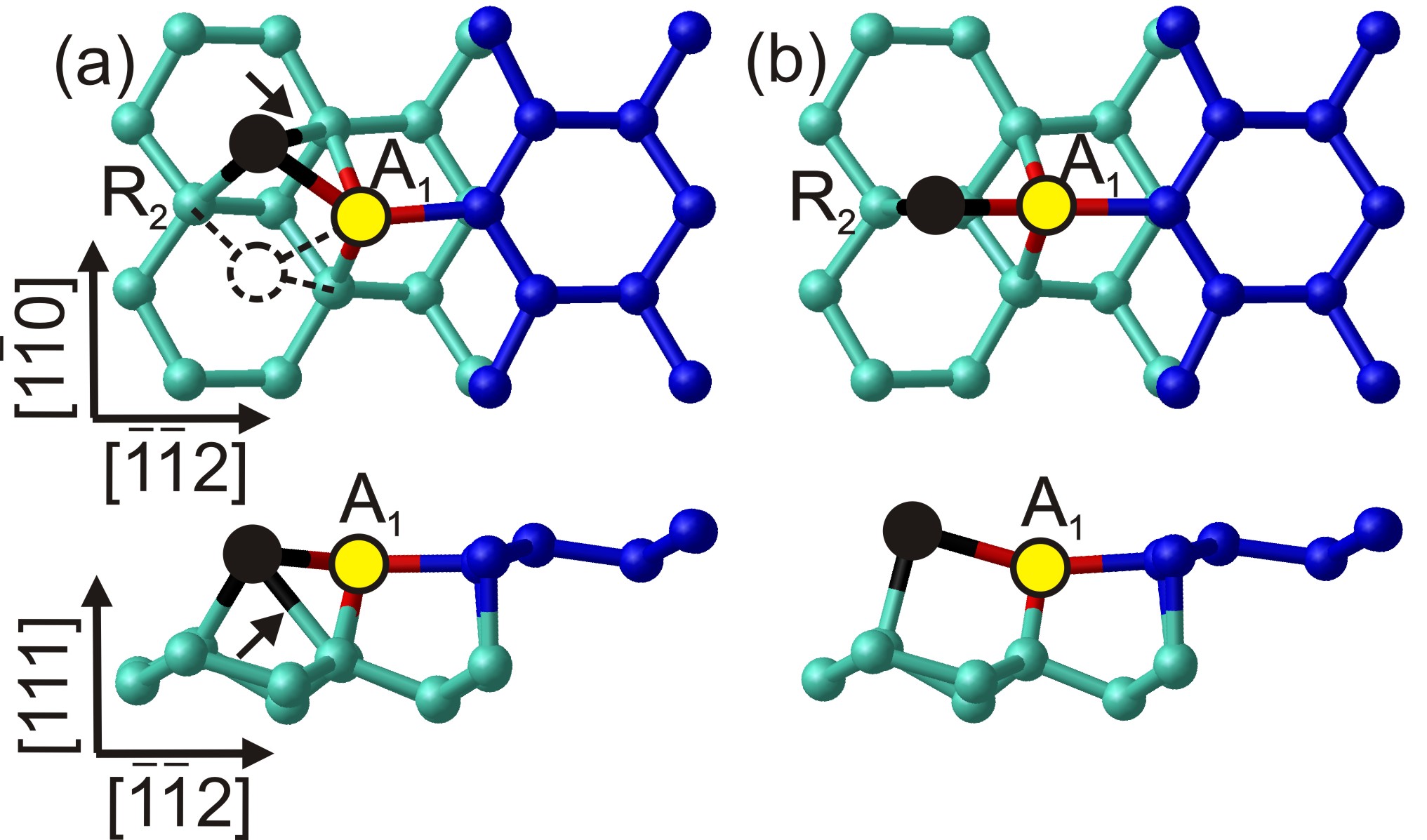
The atomic configuration related to the PES energy minima in the double well is shown in Fig. 8(a). According to this configuration, the adsorbed probe Sn atom is three-fold coordinated. The first bond is connected to the Si rest atom on the (111) terrace, the second bond is connected to the Sn adatom of the Sn atomic chain. The third bond (marked with an arrow) shares its connection to the substrate Si atom with the Sn adatom. The bond length between two Sn atoms is 2.95 Å, being very close to the calculated bond length in bulk -phase Sn (2.91 Å). The bond lengths between the Sn adatom and Si substrate are 2.76 Å, 2.72 Å, 3.02 Å, while, for the probe Sn atom, they are 2.82 Å and 3.06 Å. The longest and, therefore, weakened Sn-Si bonds of about 3 Å in each group are connected to the same five-fold coordinated (overcoordinated) Si substrate atom. When the probe Sn atom is in its saddle position, as shown in Fig. 8(b), the weak bond between this atom and the overcoordinated substrate Si atom is broken. The height change when moving the probe Sn atom from the position of energy minima to the saddle point is 0.57 Å.
For the sake of completeness, we also calculated PES for the probe Si atom on the stepped SiSn surface to check if the observed fluctuations of tunneling current in STM can be caused by trapped Si atoms. We found that the positions of energy maxima and minima on PES are very similar to the ones observed for the probe Sn atom. This is explained by the same number of valence electrons in Si and Sn atoms. However, the values of calculated local energy minima, in case of the probe Si atom, are different. It is shown in Tab. 1 that the global minimum for the probe Si atom is on the site, which is on the upper terrace just behind the adatom (Fig. 7). This result suggests that, unlike Sn atoms, Si atoms must accumulate at the upper terrace edge and be stationary at 80 K. Since this was not observed in the experimental STM images of step edges (Figs. 1(a)-1(c)), then Si adatoms can be excluded.
IV CONCLUSIONS
In summary, the structure of the single step and dynamics of adatoms on the SiSn surface were investigated by LT-STM at 80 K and ab initio calculations. The atomic model of the single steps on the SiSn surface was developed. The model contains Sn atomic chains along the step edges. The adatom dynamics was detected at the lower side of the step edge in STM at 80 K. The PES calculated using the developed step model reveals the presence of double wells at the lower side of the step edge acting as traps for adsorbed Sn atoms. The random Sn atoms trapped within the double wells and flipping between two stable states explain the fluctuating current detected in STM at 80 K.
Acknowledgements.
RAZ would like to thank the Novosibirsk State University for providing the computational resources. Cluster computations and paper writing were supported by the Russian Science Foundation (project no. 19-72-30023).References
- Wirths et al. (2016) S. Wirths, D. Buca, and S. Mantl, Prog. Cryst. Growth Charact. Mater. 62, 1 (2016).
- Maeda et al. (2015) T. Maeda, W. Jevasuwan, H. Hattori, N. Uchida, S. Miura, M. Tanaka, N. D. M. Santos, A. Vantomme, J. P. Locquet, and R. R. Lieten, Jpn. J. Appl. Phys. 54, 04DA07 (2015).
- Oehme et al. (2013) M. Oehme, D. Buca, K. Kostecki, S. Wirths, B. Holländer, E. Kasper, and J. Schulze, J. Cryst. Growth. 384, 71 (2013).
- Yu et al. (2016) K. Yu, D. L. Zhang, H. Cong, X. Zhang, Y. Zhao, B. W. Cheng, and C. B. Li, in IEEE 13th Int. Conf. Gr. IV Photonics (2016) p. 34.
- Dolbak and Olshanetsky (2008) A. E. Dolbak and B. Z. Olshanetsky, Cent. Eur. J. Phys. 6, 634 (2008).
- Lin (1995) X. W. Lin, J. Vac. Sci. Technol. B 13, 1805 (1995).
- Iwanari and Takayanagi (1992) S. Iwanari and K. Takayanagi, J. Cryst. Growth. 119, 229 (1992).
- Iwanari et al. (1992) S. Iwanari, Y. Kimura, and K. Takayanagi, J. Cryst. Growth. 119, 241 (1992).
- Takayanagi et al. (1985) K. Takayanagi, Y. Tanishiro, S. Takahashi, and M. Takahashi, Surf. Sci. 164, 367 (1985).
- Ryu et al. (2002) J. T. Ryu, T. Fujino, M. Katayama, Y. B. Kim, and K. Oura, Appl. Surf. Sci. 190, 139 (2002).
- Charrier et al. (2001) A. Charrier, R. Pérez, F. Thibaudau, J. M. Debever, J. Ortega, F. Flores, and J. M. Themlin, Phys. Rev. B 64, 115407 (2001).
- Nogami et al. (1989) J. Nogami, S. Park, and C. F. Quate, J. Vac. Sci. Technol. A 7, 1919 (1989).
- Törnevik et al. (1994) C. Törnevik, M. Göthelid, M. Hammar, U. O. Karlsson, N. G. Nilsson, S. A. Flodström, C. Wigren, and M. Östling, Surf. Sci. 314, 179 (1994).
- Törnevik et al. (1991) C. Törnevik, M. Hammar, N. G. Nilsson, and S. A. Flodström, Phys. Rev. B 44, 13144 (1991).
- Eriksson et al. (2010) P. E. J. Eriksson, J. R. Osiecki, K. Sakamoto, and R. I. G. Uhrberg, Phys. Rev. B 81, 235410 (2010).
- Levermann et al. (1996) A. H. Levermann, P. B. Howes, K. A. Edwards, H. T. Anyele, C. C. Matthai, J. E. Macdonald, R. Feidenhans’l, L. Lottermoser, L. Seehofer, G. Falkenberg, and R. L. Johnson, Appl. Surf. Sci. 104–105, 124 (1996).
- Ichikawa and Cho (2003) T. Ichikawa and K. Cho, Jpn. J. Appl. Phys. 42, 5239 (2003).
- Ressel et al. (2004) B. Ressel, C. D. Teodoro, G. Profeta, L. Ottaviano, V. Cháb, and K. C. Prince, Surf. Sci. 562, 128 (2004).
- Latyshev et al. (1992) A. V. Latyshev, A. B. Krasilnikov, and A. L. Aseev, Appl. Surf. Sci. 60–61, 397 (1992).
- Kato et al. (2000) T. Kato, T. Takajyo, H. Tochihara, and W. Shimada, Jpn. J. Appl. Phys. 39, 4307 (2000).
- Romanyuk et al. (2007) K. Romanyuk, V. Cherepanov, and B. Voigtländer, Phys. Rev. Lett. 99, 126103 (2007).
- Voigtländer (2001) B. Voigtländer, Surf. Sci. Rep. 43, 127 (2001).
- Teys et al. (2014) S. A. Teys, K. N. Romanyuk, and B. Z. Olshanetsky, J. Cryst. Growth. 404, 39 (2014).
- Rogilo et al. (2013) D. I. Rogilo, L. I. Fedina, S. S. Kosolobov, B. S. Ranguelov, and A. V. Latyshev, Phys. Rev. Lett. 111, 036105 (2013).
- Ronci et al. (2005) F. Ronci, S. Colonna, S. D. Thorpe, A. Cricenti, and G. LeLay, Phys. Rev. Lett. 95, 156101 (2005).
- Ronci et al. (2007) F. Ronci, S. Colonna, A. Cricenti, and G. LeLay, Phys. Rev. Lett. 99, 166103 (2007).
- Ronci et al. (2010) F. Ronci, S. Colonna, A. Cricenti, and G. LeLay, J. Phys.: Condens. Matter 22, 264003 (2010).
- Troullier and Martins (1991) N. Troullier and J. L. Martins, Phys. Rev. B 43, 1993 (1991).
- Soler et al. (2002) J. M. Soler, E. Artacho, J. D. Gale, A. García, J. Junquera, P. Ordejón, and D. Sánchez-Portal, J. Phys.: Condens. Matter 14, 2745 (2002).
- Perdew et al. (1996) J. P. Perdew, K. Burke, and M. Ernzerhof, Phys. Rev. Lett. 77, 3865 (1996).
- Flores et al. (2001) F. Flores, J. Ortega, R. Pérez, A. Charrier, F. Thibaudau, J. M. Debever, and J. M. Themlin, Prog. Surf. Sci. 67, 299 (2001).
- Profeta and Tosatti (2007) G. Profeta and E. Tosatti, Phys. Rev. Lett. 98, 086401 (2007).
- Modesti et al. (2007) S. Modesti, L. Petaccia, G. Ceballos, I. Vobornik, G. Panaccione, G. Rossi, L. Ottaviano, R. Larciprete, S. Lizzit, , and A. Goldoni, Phys. Rev. Lett. 98, 126401 (2007).
- Schuwalow et al. (2010) S. Schuwalow, D. Grieger, and F. Lechermann, Phys. Rev. B 82, 035116 (2010).
- Monkhorst and Pack (1976) H. J. Monkhorst and J. D. Pack, Phys. Rev. B 13, 5188 (1976).
- Tersoff and Hamann (1985) J. Tersoff and D. R. Hamann, Phys. Rev. B 31, 805 (1985).
- Kohn and Sham (1965) W. Kohn and L. J. Sham, Phys. Rev. 140, A1133 (1965).
- Horcas et al. (2007) I. Horcas, R. Fernández, J. M. Gómez-Rodríguez, J. Colchero, J. Gómez-Herrero, and A. M. Baro, Rev. Sci. Instrum. 78, 013705 (2007).
- Battaglia et al. (2008) C. Battaglia, P. Aebi, and S. C. Erwin, Phys. Rev. B 78, 075409 (2008).
- Avila et al. (1999) J. Avila, A. Mascaraque, E. G. Michel, M. C. Asensio, G. LeLay, J. Ortega, R. Pérez, and F. Flores, Phys. Rev. Lett. 82, 442 (1999).
- Gori et al. (2009) P. Gori, F. Ronci, S. Colonna, A. Cricenti, O. Pulci, , and G. LeLay, EPL 85, 66001 (2009).
- Chang and Wei (2003) C. M. Chang and C. M. Wei, Phys. Rev. B 67, 033309 (2003).
- Zhachuk et al. (2010) R. Zhachuk, B. Olshanetsky, J. Coutinho, and S. Pereira, Phys. Rev. B 81, 165424 (2010).