Mirror symmetric on-chip frequency circulation of light
Abstract
Integrated circulators and isolators are important for developing on-chip optical technologies, such as laser cavities, communication systems, and quantum information processors. These devices appear to inherently require mirror symmetry breaking to separate backwards from forwards propagation, so existing implementations rely upon magnetic materials, or interactions driven by propagating waves. In contrast to previous work, we demonstrate a mirror symmetric nonreciprocal device. Our device comprises three coupled photonic resonators implemented in thin-film lithium niobate. Applying radio frequency modulation, we drive conversion between the frequency eigenmodes of this system. We measure nearly 40 dB of isolation for approximately 75 mW of RF power near 1550 nm. We simultaneously generate nonreciprocal conversion between all of the eigenmodes in order to demonstrate circulation. Mirror symmetric circulation significantly simplifies the fabrication and operation of nonreciprocal integrated devices. Finally, we consider applications of such on-chip isolators and circulators, such as full-duplex isolation within a single waveguide.
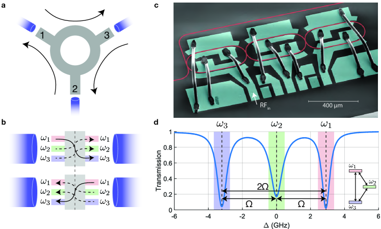
Circulators are nonreciprocal devices that allow propagating signals to cycle between three channels, e.g., as shown in Fig 1a. A circulator can isolate components from each other, i.e., it can prevent reflections from returning to the source of a signal, simply by terminating one of its three channels through absorption. For example if we terminate port in Fig. 1a, signals will propagate from , but would be terminated, thereby preventing reflections on the third port from propagating back to the first port. There is flexibility in selecting the input and output channels. In many realizations, the channels are the incoming and outgoing waves in the waveguides connected to port . However, other realizations are also possible. In this work, our input channels correspond to the incoming waves at different frequencies in one waveguide (on the left in Fig. 1b), and the output channels correspond to the outgoing waves at different frequencies in the other side of the waveguide (on the right in Fig. 1b). Unlike more typical three-waveguide configurations, this type of circulator is compatible with mirror symmetry Wang et al. (2021): by imposing the same scattering relations between the frequency channels for light traveling from right to left in the device, we obtain a second frequency circulation, related to the first by reflection about the center axis (dashed line in Fig. 1b).
The mirror symmetry of our circulator means that its physical implementation can be simpler than more traditional circulators and isolators, which require mirror symmetry breaking. Many of these demonstrations use magnetic materials Bi et al. (2011); Tzuang et al. (2014); Srinivasan and Stadler (2018); Huang et al. (2016); Yan et al. (2020); Sobu et al. (2013), traveling waves Kittlaus et al. (2018, 2021); Kim et al. (2021); Shen et al. (2016); Ruesink et al. (2016); Kang et al. (2011); Kim et al. (2015); Dong et al. (2015); Hafezi and Rabl (2012); Tian et al. (2021); Sohn et al. (2021), or multiple modulators emitting with different phases Fang et al. (2012); Lira et al. (2012); Doerr et al. (2011); Yu and Fan (2009); Dostart et al. (2021) to induce a sense of direction and nonreciprocal propagation. As a consequence of mirror symmetry in our device, a single radio frequency (RF) electro-optic modulator (EOM) is sufficient to generate circulation between three optical frequency channels. As we show here, this significantly simplifies hardware implementations of nonreciprocal photonic circuits.
Results
We demonstrate a device on a thin film lithium niobate (TFLN) platform that consists of three coupled photonic racetrack resonators. The first resonator is coupled to a bus waveguide, as shown in Fig. 1c. The modes of racetrack resonators () and () are coupled at a rate (), while and are not directly coupled (). Our device uses the guided mode, which on X-cut TFLN has large electro-optic coupling to fields parallel to both the chip surface and the crystal Z axis. Electrodes fabricated across each racetrack enable independent DC bias tuning of the uncoupled or bare mode frequencies via the linear electro-optic effectWeis and Gaylord (1985). This is necessary to counteract drift and fabrication disorder.
We set the desired operating point by using the DC bias to tune all of the bare mode frequencies to be equal, which yields three evenly spaced resonances in the coupled or dressed basis with frequencies . In an ideal system, the spacing is with . These three resonances couple to the bus waveguide through their spatial overlaps with the first racetrack and therefore lead to dips in the transmission spectrum, as shown in Fig. 1d. This overlap also means that RF modulation of the racetrack adjacent to the bus waveguide couples all three resonances together, as depicted by the schematic three-level system in Fig. 1d.
We apply an RF modulation of the form:
| (1) |
The frequency corresponds to the microwave modulation frequency. In an ideal system with equal inter-modal couplings , we would set to . Fabrication disorder and tuning imprecision means that the ’s are slightly different. For example, and , as inferred for the data in Fig. 1d, so we drive at , the average of the difference between the measured coupled resonance frequencies and . Driving at scatters light between dressed modes and , whereas the drive scatters light between modes and . For any pair of dressed modes, two possible transition pathways exist, as depicted by the schematic inset in Fig. 1d. One pathway is a direct transition, whereas the other is a two-step transition through the third mode. By varying the amplitudes and relative phases of the two RF tones, we enhance or suppress different pathways by generating interference. In the ideal disorder-free model, forward isolation (mode ) is maximized for the phase condition .
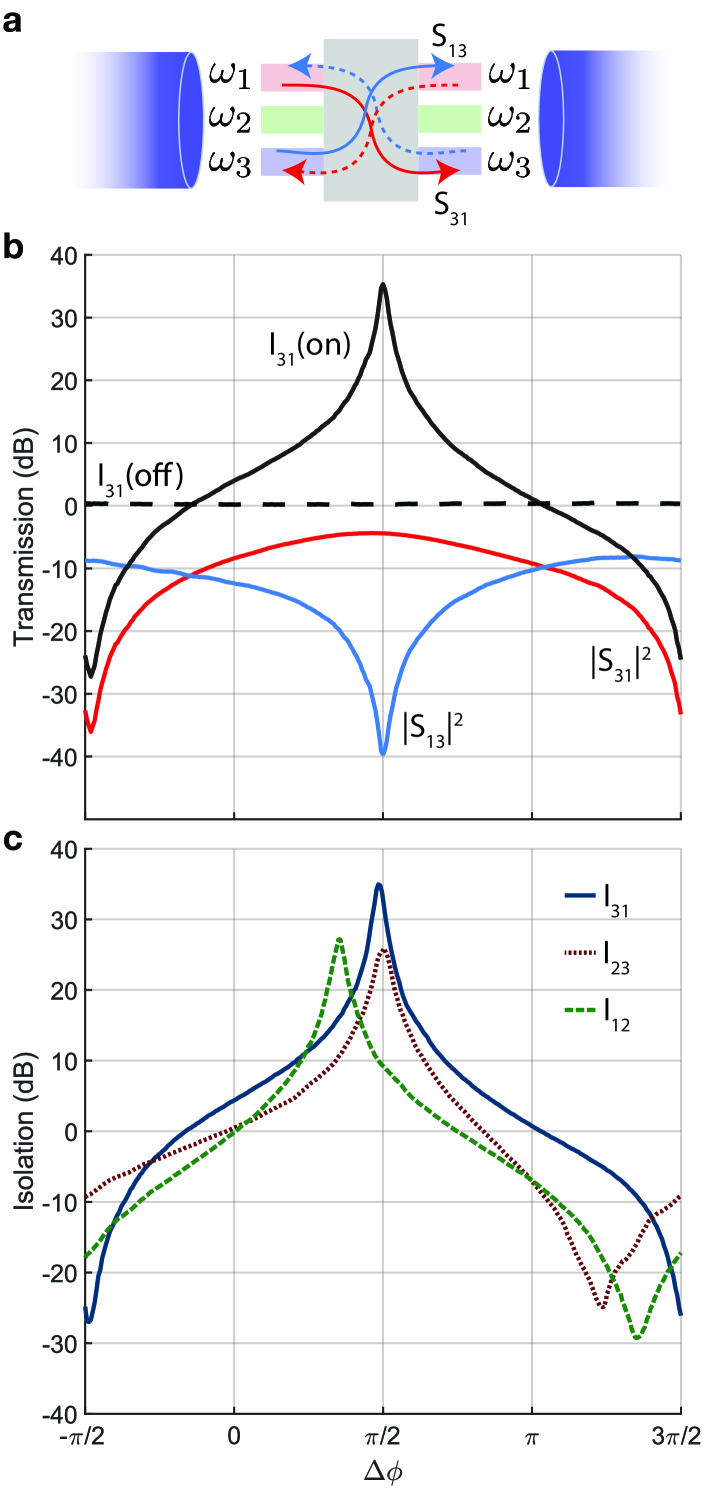
We characterize the performance of our circulator by measuring the scattering parameters , which quantify how the amplitude of each incoming wave at frequency is converted to the amplitude of an outgoing wave at frequency , propagating in the same direction in the opposite waveguide. This is depicted in Fig. 2a. We define an isolation parameter as
This characterizes the asymmetry between forward and backward frequency conversion for a pair of modes. As shown in Fig. 2b for channels and , it is clear that forward scattering from occurs efficiently while the backward scattering is strongly suppressed. This leads to approaching when the driving phase condition is and are correctly tuned, as explained below. Similar isolation is observed for other pairs of channels.
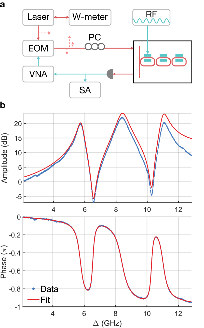
We obtain the scattering and isolation parameters described above by first characterizing the device’s linear spectrum, with the RF modulation turned off. We measure the optical transmission parameter as a function of frequency, which we then use to infer and DC-tune the device’s parameters. This transmission amplitude evaluated at frequencies corresponds to since it describes transmission through the device without a change in frequency. We place a laser tone at frequency , blue-detuned from all of the resonances, and feed it through a commercial electro-optic modulator (EOM) before sending it to the device. Driving the EOM with a vector network analyzer (VNA), we generate two sidebands at . By sweeping the VNA modulation frequency, we move one sideband across the cavity response, which then beats against the optical feed-through, , on a subsequent RF photodiode connected to the VNA. Sweeping the VNA frequency allows us to see, nearly in real-time, the hybridized mode structure of the device, as shown in Fig. 3b. Our device exhibits DC bias drift as a result of photorefraction, a common challenge in lithium niobate devicesMcKenna et al. (2020); Jiang et al. (2017); Xu et al. (2021). This measurement technique enables us to observe and compensate for these changes as the optical input power and DC bias both affect the spectrum. We fit a complete model of the measurement, including the EOM transmission, cavity response, and phase response measured by the VNA in order to determine all of the device’s optical parameters (loss rates, resonant frequencies, etc.). An example of such a fit is depicted in Fig. 3c. We can also extract the sideband transmission from these spectra.
We then measure the “active” device by turning on the RF drive and characterizing the scattering between frequency channels. Since VNA measurements only find linear scattering parameters, characterizing the scattering between frequencies requires a different measurement scheme than that described above. Keeping the laser at , we modulate the EOM at frequency in order to generate and input light at frequency . We infer all of the optical powers in the different channels by making RF measurements of their beating against the feed-through light at . This presents a minor complication for inferring , as the beat notes generated by both EOM sidebands interfere at RF frequency . This ambiguity can be resolved by comparing measurements of to the independently measured scattering parameters (see previous paragraph) when RF modulation to the chip is turned off. Note that the other scattering parameters can be inferred without this complication, so the isolation parameters are unaffected. For all scattering parameters, we record the RF power in the beat note corresponding to optical frequency , while varying the RF phase . This power is proportional to . We take the ratio of the measured power in to that of the unmodulated transmission at the signal frequency . By factoring out the contribution from the non-resonant input tone at , we obtain the scattering parameters (see SI).
The scattering parameter measurements shown in Fig. 2 are taken for optimized values of the RF drive amplitude . When the RF drive is turned down, i.e., , but the drive is kept on, we do not observe isolation (dashed line in Fig. 2b). For tuned values of and , we observe simultaneous isolation between the three pairs of dressed frequencies, demonstrating circulator-like behavior, as depicted in Fig. 2c.
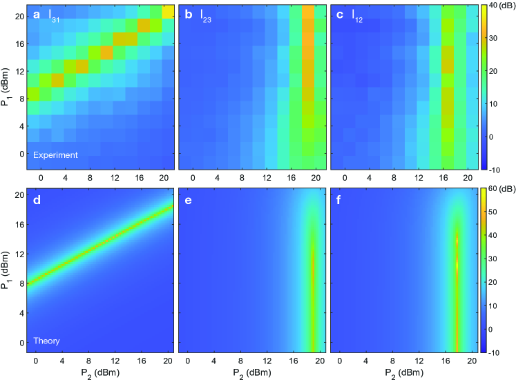
We next characterize the RF power-dependent operation of our device by varying the modulation amplitudes and . For each power combination, we sweep the phase condition of the RF sources through multiple periods and extract the peak isolation observed for each transition. We generate maps of the isolation versus RF power, depicted in Fig. 4a-c. Each pixel is normalized by linear scattering parameters, analogously to the data in Fig. 2. The optical device characteristics used for this normalization are extracted from the VNA trace in Fig. 3, taken prior to varying the RF power.
Figures 4d-f depict theoretical plots of device performance obtained from coupled mode theory and show good agreement with the measured trends. We attribute differences between theory and experiment, such as the slopes in the maps and the locations of peak isolation in and , to mode drifts over the full course of measurement. This drift could emerge from either DC bias drift, which introduces disorder in the mode hybridization, or from high-power RF-induced drift (see SI). We assume this drift does not significantly affect the normalization factor we use for data processing, which is obtained from the initial VNA trace. From the theoretical plots, we infer a high-frequency bare mode modulation rate MHz. This rate closely matches the directly measured low-frequency modulation rate MHz.
We can understand the trends in the isolation factor RF power dependence by studying the coupled mode theory description of the dynamicsWang et al. (2021). The RF modulation scatters photons between the dressed modes at a rate proportional to , where is the electro-optic tuning of the bare RF-coupled mode. We observe strong enhancement in in Fig. 4a,d along a locus corresponding to . This condition is found by noting that for cancellation to occur, the rate at which direct scattering occurs, , needs to match the rate of indirect scattering , which is approximately 111By second-order perturbation theory.. Here, is the linewidth (full-width, half-max – FWHM) of the second dressed mode. A more detailed analysisWang et al. (2021) indicates that maximum isolation is given by:
where .
A similar line of reasoning explains the large isolation regions in Fig. 4b,c,e,f. For example, note that a peak requires interference between two scattering processes – a direct process , occurring with a rate , and an indirect process , occurring at a rate . This interference is maximized when the rates are nearly equal. A more detailed coupled mode analysis confirms that the ideal condition , where , maximizes the isolation parameter. The isolation parameters and are therefore maximized when:
independently of the direct scattering rate . Inhomogeneity in the mode hybridization causes deviations from this exact condition for versus , i.e., they appear at slightly different power conditions in Fig. 4b,c.
Discussion
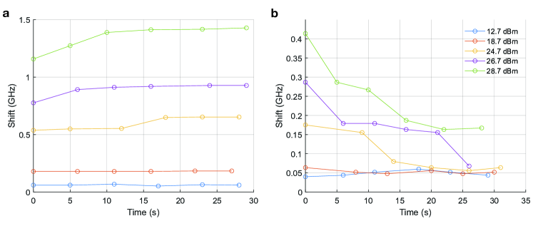
Our platform’s most significant limit is due to optical loss in the cavities. In the ideal realization the dressed mode linewidths are entirely due to coupling out into the feed waveguide. When the RF drives are off, the absence of intrinsic loss means that the dressed modes are overcoupled, so . As we increase the RF driving power, the scattering between dressed modes appears as additional loss at the signal frequency. This moves the mode from being over-coupled into a critically coupled condition, when the scattering-induced loss at mode equals the mode’s coupling rate to the waveguide and leads to . However, in the experimentally realized system, there is additional intrinsic loss in all three cavities, and the dressed modes are already close to being critically coupled when the RF drives are off. The RF induced scattering then acts to increase transmission as it moves the mode farther away from being critically coupled. This means that in contrast to the ideal circulator, the diagonal elements of the scattering matrix are nonzero in our realization. We expect that with improvements in optical of on-chip LN devices, this problem can be largely eliminated Shams-Ansari et al. (2021). One possible way to circumvent this challenge in the shorter term is to include an additional resonator after the device at frequency in order to filter out any feed-through and make for a single channel. Another approach that does not require major improvements in the is to increase the cavity-waveguide coupling and start within a more over-coupled regime. However, this approach would require larger RF powers and we are already power-limited. The off-chip microwave amplifier saturates at approximately dBm. Moreover, as power to the device increases above roughly mW, we observe dressed mode drifts on the order of MHz, which disrupts the resonance condition required for high isolation (see SI).
Another limit of our approach is due to its resonant nature. The isolation bandwidth of our device depends on the dressed mode linewidths, and we measured sustained isolation over more than a few hundred megahertz. This too can be increased, but at the cost of greater RF power as the also scale with bandwidth. One strategy to make the modulation more efficient would be to include modulation into the third racetrack. Alternatively, since we only need narrowband RF modulation, we could use the extremely efficient optomechanical modulation schemes recently demonstrated on LN Jiang et al. (2020a); Shao et al. (2019); Sarabalis et al. (2020) to significantly reduce the needed RF power and realize larger bandwidth. Finally, we note that the bandwidth of the device is potentially larger than the linewidth of a single mode as there are families of modes repeating with the cavity free spectral range, and under low disorder, these would also behave as circulators for signals at different sets of frequencies.
A novel feature of our device is its operation as a bi-directional isolator – a property that emerges from mirror symmetry and frequency-domain operation. For example, two transmitters/receivers can operate simultaneously along a single channel. Node can transmit a signal down a waveguide at frequency to node , who recieves at . This communication is isolated. Meanwhile, node can then send a signal backwards along the waveguide at to node , who also receives at . This communication is also isolated. With the standard optical isolator, this behavior would require two optical channels, one for each direction of transmission.
Overall, we have demonstrated an integrated frequency isolator/circulator on thin-film lithium niobate, an emerging platform for classical and quantum photonics. We measured peak isolation of nearly dB with dB insertion loss for dual RF drive powers of mW mW. Our device is reconfigurable, enabling isolation over a wide range of powers for different operating frequencies. For example, we also measure isolation of more than dB for dual RF powers of mW and mW, but with a commensurate increase of insertion loss ( dB). Furthermore, we also measured insertion loss as low as dB for different power and isolation conditions. Ultimately, the mirror symmetry and frequency-domain operation of our device provide for novel applications as an isolator/circulator and frequency router in photonic circuits.
Methods
Fabrication. The device is fabricated in a two-mask process from 500 nm-thick film of lithium niobate (LN) atop a sapphire (Sa) handle. The components are air-clad, and the electrodes are fabricated as a Ti:Au metal bilayer. The first mask, for photonics fabrication, is defined from hydrogen silsequioxane (HSQ), a negative-tone electron beam resist, patterned with 100 kV electron beam lithography (JEOL JBX-6300FS). We transfer the patterns into the LN with argon ion mill etching (IntlVac ion mill), followed by an acid cleaning procedure. We confirm the device’s optical performance prior to fabricating electrodes. The electrodes are defined with a standard photoresist lift-off bilayer. The patterns are written using direct-write lithography (Heidelberg MLA150), and metal is evaporated (Kurt J. Lesker LAB18) prior to solvent-based liftoff. Lastly, we wirebond on-chip to connect electrodes across the optics, thereby defining proper modulation polarity on-chip (West Bond 7476E).
Characterization. The device is optically pumped from a telecommunications wavelength diode laser (Santec TSL-550). We lock the optical pump blue-detuned from the modes at 1543.6 nm (via a Bristol Wavemeter). The light is passed through a polarization control wheel and in-line fiber polarizer to maximize TE transmission. This light is passed into a commercial electro-optic amplitude modulator (EOM). We drive the EOM from a VNA (R&S ZNB20) in order to generate sidebands. The pump and sidebands are then passed through another polarization controller, into a variable optical attenuator (VOA), then a power meter before being passed onto the chip. By sweeping the frequency of the VNA output (or by driving a particular frequency) we can sweep the sideband across (or directly drive) the optical dressed modes of the system. The light undergoes modulation on-chip. Output light from the optical waveguide passes through an erbium-doped fiber amplifier (EDFA) and an X-switch, which switches our detector between a photodiode for linear optical characterization, and a fast photo-diode (Optilab PD-40M), which records beat tones between the optical pump, the EOM sideband, and converted sidebands when applying on-chip modulation. The output of the fast photo-diode passes through a bias-tee. One arm passes back to the VNA to record the broad-band response of the cavity, and the other arm passes to a spectrum analyzer (R&S FSW26) to record converted sideband powers with high precision. This setup enables us to simultaneously observe the full cavity response on the VNA in nearly real-time while adjusting DC bias across the device and manipulating the optical pump, while also observing sideband powers at particular frequencies when driving on-chip modulation.
In order to characterize our device mirror symmetry, we separately insert a second X-switch and polarization control just before the device. We record transmission through the device from both waveguide propagation directions, demonstrating equivalence of scattering matrix elements (see SI).
On-chip modulation is driven from two pulsed signal generators (PSG, Keysight E8257D). One PSG drives the tone while the other drives the tone. We vary the relative phase between these sources. The clocks of the PSGs are locked together, and these are in turn locked to the clock of the FSW26. The two PSG outputs are combined at a power splitter and passed through a high-power microwave amplifier. The output of the amplifier is then passed to a probe, which is contacted to the on-chip electrical pads. Importantly, the rate of direct phase modulation on the PSG is much faster than the global phase drift of the system, enabling us to visualize power modulations at sideband frequencies on the FSW26.
Author contribution. J.F.H. fabricated the device. J.F.H. and V.A. led the experimental effort. J.W. developed the device operating theory and characterized theoretical device performance. J.F.H, J.D.W., and J.W. determined physical device designs. J.D.W. assisted in early experimentation. A.H.S.N and S.F. provided experimental and theoretical guidance and support for this experiment.
Acknowledgements
J.F.H. acknowledges support from the National Science Foundation Graduate Research Fellowship Program (Grant No. DGE-1656518). V.A. acknowledges support by the Stanford Q-FARM Bloch Fellowship Program. The authors acknowledge the support of an AFOSR MURI project (FA9550-18-1-0379), the National Science Foundation under award ECCS-1820938, and the Defense Advanced Research Projects Agency (DARPA) LUMOS program. Part of this work was performed at the Stanford Nano Shared Facilities (SNSF), supported by the National Science Foundation under award ECCS-2026822. Work was performed in part in the nano@stanford labs, which are supported by the National Science Foundation as part of the National Nanotechnology Coordinated Infrastructure under award ECCS-1542152. The authors would like to thank Wentao Jiang and Christopher J. Sarabalis for insightful and helpful discussions.
References
- Wang et al. (2021) J. Wang, J. F. Herrmann, J. D. Witmer, A. H. Safavi-Naeini, and S. Fan, Phys. Rev. Lett. 126, 193901 (2021).
- Bi et al. (2011) L. Bi, J. Hu, P. Jiang, D. H. Kim, G. F. Dionne, L. C. Kimerling, and C. Ross, Nature Photonics 5, 758 (2011).
- Tzuang et al. (2014) L. D. Tzuang, K. Fang, P. Nussenzveig, S. Fan, and M. Lipson, Nature photonics 8, 701 (2014).
- Srinivasan and Stadler (2018) K. Srinivasan and B. J. Stadler, Optical Materials Express 8, 3307 (2018).
- Huang et al. (2016) D. Huang, P. Pintus, C. Zhang, Y. Shoji, T. Mizumoto, and J. E. Bowers, IEEE Journal of Selected Topics in Quantum Electronics 22, 271 (2016).
- Yan et al. (2020) W. Yan, Y. Yang, S. Liu, Y. Zhang, S. Xia, T. Kang, W. Yang, J. Qin, L. Deng, and L. Bi, Optica 7, 1555 (2020).
- Sobu et al. (2013) Y. Sobu, Y. Shoji, K. Sakurai, and T. Mizumoto, Opt. Express 21, 15373 (2013).
- Kittlaus et al. (2018) E. A. Kittlaus, N. T. Otterstrom, P. Kharel, S. Gertler, and P. T. Rakich, Nature Photonics 12, 613 (2018).
- Kittlaus et al. (2021) E. A. Kittlaus, W. M. Jones, P. T. Rakich, N. T. Otterstrom, R. E. Muller, and M. Rais-Zadeh, Nature Photonics 15, 43 (2021).
- Kim et al. (2021) S. Kim, D. B. Sohn, C. W. Peterson, and G. Bahl, APL Photonics 6, 011301 (2021).
- Shen et al. (2016) Z. Shen, Y.-L. Zhang, Y. Chen, C.-L. Zou, Y.-F. Xiao, X.-B. Zou, F.-W. Sun, G.-C. Guo, and C.-H. Dong, Nature Photonics 10, 657 (2016).
- Ruesink et al. (2016) F. Ruesink, M.-A. Miri, A. Alu, and E. Verhagen, Nature communications 7, 1 (2016).
- Kang et al. (2011) M. S. Kang, A. Butsch, and P. S. J. Russell, Nature Photonics 5, 549 (2011).
- Kim et al. (2015) J. Kim, M. C. Kuzyk, K. Han, H. Wang, and G. Bahl, Nature Physics 11, 275 (2015).
- Dong et al. (2015) C.-H. Dong, Z. Shen, C.-L. Zou, Y.-L. Zhang, W. Fu, and G.-C. Guo, Nature communications 6, 1 (2015).
- Hafezi and Rabl (2012) M. Hafezi and P. Rabl, Optics express 20, 7672 (2012).
- Tian et al. (2021) H. Tian, J. Liu, A. Siddharth, R. N. Wang, T. Blésin, J. He, T. J. Kippenberg, and S. A. Bhave, arXiv preprint arXiv:2104.01158 (2021).
- Sohn et al. (2021) D. Sohn, O. E. Örsel, and G. Bahl, arXiv preprint arXiv:2104.04803 (2021).
- Fang et al. (2012) K. Fang, Z. Yu, and S. Fan, Physical review letters 108, 153901 (2012).
- Lira et al. (2012) H. Lira, Z. Yu, S. Fan, and M. Lipson, Physical review letters 109, 033901 (2012).
- Doerr et al. (2011) C. R. Doerr, N. Dupuis, and L. Zhang, Optics letters 36, 4293 (2011).
- Yu and Fan (2009) Z. Yu and S. Fan, Nature Photonics 3, 91 (2009).
- Dostart et al. (2021) N. Dostart, H. Gevorgyan, D. Onural, and M. A. Popović, Optics Letters 46, 460 (2021).
- Weis and Gaylord (1985) R. S. Weis and T. K. Gaylord, Applied Physics A. , 191 (1985).
- McKenna et al. (2020) T. P. McKenna, J. D. Witmer, R. N. Patel, W. Jiang, R. van Laer, P. Arrangoiz-Arriola, E. A. Wollack, J. F. Herrmann, and A. H. Safavi-Naeini, Optica 7, 1737 (2020).
- Jiang et al. (2017) H. Jiang, R. Luo, H. Liang, X. Chen, Y. Chen, and Q. Lin, Opt. Lett. 42, 3267 (2017).
- Xu et al. (2021) Y. Xu, M. Shen, J. Lu, J. B. Surya, A. A. Sayem, and H. X. Tang, Opt. Express 29, 5497 (2021).
- Note (1) By second-order perturbation theory.
- Shams-Ansari et al. (2021) A. Shams-Ansari, G. Huang, L. He, M. Churaev, P. Kharel, Z. Tan, J. Holzgrafe, R. Cheng, D. Zhu, J. Liu, B. Desiatov, M. Zhang, T. J. Kippenberg, and M. Lončar, in Conference on Lasers and Electro-Optics (Optical Society of America, 2021) p. STh4J.4.
- Jiang et al. (2020a) W. Jiang, C. J. Sarabalis, Y. D. Dahmani, R. N. Patel, F. M. Mayor, T. P. McKenna, and R. van Laer amd Amir H. Safavi-Naeini, Nature Communications 1166 (2020a), https://doi.org/10.1038/s41467-020-14863-3.
- Shao et al. (2019) L. Shao, M. Yu, S. Maity, N. Sinclair, L. Zheng, C. Chia, A. Shams-Ansari, C. Wang, M. Zhang, K. Lai, and M. Lončar, Optica 6, 1498 (2019).
- Sarabalis et al. (2020) C. J. Sarabalis, T. P. McKenna, R. N. Patel, R. Van Laer, and A. H. Safavi-Naeini, APL Photonics 5, 086104 (2020), https://doi.org/10.1063/5.0012288 .
- Patel et al. (2018) R. N. Patel, Z. Wang, W. Jiang, C. J. Sarabalis, J. T. Hill, and A. H. Safavi-Naeini, Phys. Rev. Lett. 121, 040501 (2018).
- Williamson et al. (2020) I. A. Williamson, M. Minkov, A. Dutt, J. Wang, A. Y. Song, and S. Fan, Proceedings of the IEEE 108, 1759 (2020).
- Jiang et al. (2020b) W. Jiang, C. J. Sarabalis, Y. D. Dahmani, R. N. Patel, F. M. Mayor, T. P. McKenna, R. Van Laer, and A. H. Safavi-Naeini, Nature Communications 11, 1166 (2020b).
Supplementary Information: Mirror symmetric on-chip frequency circulation of light
S1 Fitting EOM Response
S1.1 Cavity Response and Coupled Eigenmodes
We derive the cavity response in the bare-mode basis according to standard coupled mode theory. In the following, describes the total decay rate of bare mode , is the coupling between bare modes and , and is the extrinsic coupling rate of the first ring coupled to the waveguide (). The triple-ring system is described by the Hamiltonian:
-
•
-
•
-
•
We take the Heisenberg equations of motion to arrive at the coupled mode theory for the three resonances, :
| (1a) | ||||
| (1b) | ||||
| (1c) | ||||
| (1d) | ||||
We go into a frame rotating with the laser frequency, . This shifts our resonances relative to the drive tone, . Fourier transforming into the frequency domain and taking , we obtain the eigenvalue equation 2.
| (2) |
Here, . The real part of the eigenvalues corresponds to the dressed mode frequencies , and the dressed mode loss rates are twice the magnitude of the imaginary part.
Taking the Fourier Transform of the equations of motion has the effect of the following further substitutions:
(and similarly for modes 2,3). We solve the Fourier transformed equations 1 for the linear cavity transmission in the frame rotating with the laser:
| (3) |
S1.2 EOM Response
We calculate the photodiode response to light modulated by an EOM traveling through our devicePatel et al. (2018). An intensity modulator can be described as a beam-splitter, followed by a variable phase shift on one path, followed by a second beam-splitter. This is given by the following.
| (4) |
In the above, is the laser input in the rotating frame of the laser. Furthermore, describe asymmetric loss between the arms of the integrated modulator. The phase accumulated in the EOM is given by a DC phase shift, , plus harmonic modulation:
| (5) |
is small, so we can neglect higher-order sidebands. We solve for the time-dependent transmission through the EOM:
| (6) |
In our experiment, the laser is blue-detuned from the cavity, so the sideband sweeps across a mode as we sweep the modulation frequency . The carrier and both sidebands are then filtered by the linear cavity response in eq. 3 to yield the time-dependent transmission through our device. This leads to an output field amplitude:
| (7) |
This transmitted field is recorded on a photodiode and routed to a VNA. We AC-couple the output to neglect DC offsets:
| (8) |
The voltage from the photodiode is given by , and the VNA trace is proportional to the amplitude of the comlex number .
We normalize by the far-detuned response (), which allows us to cancel pre-factors corresponding to the carrier tone amplitude, RF modulation amplitude, global phases, and frequency-dependent cable and detector losses. We can fit the normalized phase response of the VNA () to determine system parameters.
| Parameter | Description | Average | 95% Confidence Interval |
|---|---|---|---|
| Wavelength of laser drive | nm | - | |
| Extrinsic loss rate of the first resonator | MHz | MHz | |
| Intrinsic loss rate of the first resonator | MHz | MHz | |
| First resonator total loss rate () | GHz | GHz | |
| Second resonator total loss rate | MHz | MHz | |
| Third resonator total loss rate | MHz | MHz | |
| Coupling rate between first and second resonators | GHz | GHz | |
| Coupling rate between second and third resonators | GHz | GHz | |
| Detuning of first bare mode from laser drive | GHz | GHz | |
| Detuning of second bare mode from laser drive | GHz | GHz | |
| Detuning of third bare mode from laser drive | GHz | GHz | |
| Detuning of third dressed mode from laser drive | GHz | GHz | |
| Detuning of second dressed mode from laser drive | GHz | GHz | |
| Detuning of first dressed mode from laser drive | GHz | GHz | |
| RF drive frequency | GHz | - | |
| RF power used in below detuning study | 73.2 mW | - | |
| RF power used in below detuning study | 59.0 mW | - | |
| High frequency bare mode modulation rate (inferred) | 330 MHz/V | - | |
| Low frequency bare mode modulation rate (measured) | 328.5 MHz/V | - |
S1.3 Bootstrapping: System Parameters
Our model has many free parameters, so our fit quality is sensitive to an initial guess. We account for this by applying a modified bootstrap algorithm. We repeatedly fit subsets of the VNA trace using random parameter guesses within physical bounds. We obtain distributions of the fit parameters, summarized in table S1. After fitting , , , we can solve eq. 2 for the dressed mode detunings, , from the carrier tone. We generate input signals at dressed mode frequencies by driving the EOM at . When the EOM DC bias phase , the VNA trace appears symmetric, and we can approximate the super-mode locations by extracting the peaks in the VNA trace. In order to improve the symmetry of the mode transitions in the conversion experiment, we apply RF modulation at , and we position the input at GHz.
S2 Scattering Matrix Formalism
S2.1 Normalization and Scattering Parameters
In order to establish non-reciprocity, we must demonstrate that the scattering matrix describing input and output of the device is asymmetricWilliamson et al. (2020). We first consider the forward (left-to-right) propagating modes. In the main text, we describe our measurement procedure to obtain scattering matrix elements. We measure the linear transmission amplitude, corresponding to un-modulated signal light, . The power recorded through the photodiode onto an FSW, includes contributions from both the resonant EOM sideband (i.e., the signal input at frequency ) and the non-resonant sideband (). The measured power is related to the input signal amplitude by a normalization factor: . Turning on RF modulation, we measure the converted sideband amplitudes . Scattering is given by the expression:
| (9) |
The power in a given sideband is proportional to the integration of the autocorrelation function , which is recorded on the FSW. This integration is proportional to from 8. We therefore measure sideband power as a function of the transmitted signal power:
| (10) |
We identify such that we factor out the non-resonant sideband contribution in 10.
| (11) |
All of the free parameters in equations 10 and 11 are obtained via the fits demonstrated in section S1.3. The diagonal elements also contain a non-resonant contribution in the transmitted power measurement, so they require a slightly modified normalization factor.
For a fixed phase condition, , and modulation amplitudes, mW and mW, the scattering matrix takes on an asymmetric form demonstrating circulation. The diagonal elements correspond to feedthrough at the original signal frequency as described in the main text. Here we present the scattering matrices for both forward () and reverse () circulation for left-to-right-propagating signals.
| (12) |
| (13) |
The scattering matrices are asymmetric, thereby demonstrating non-reciprocal frequency conversion and amplitude transmission between the frequency ports. Diagonal elements correspond to feed-through at the original signal frequencies, which can be reduced using techniques discussed in the main text.
S2.2 Forward and Reverse Isolation
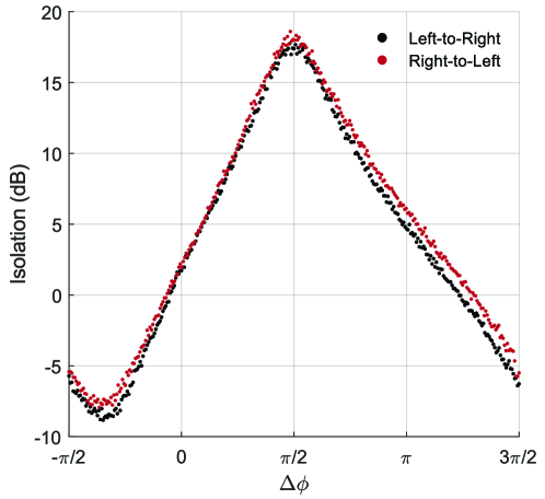
We confirm mirror symmetry in our device by measuring and comparing isolation for light propagating from left-to-right versus right-to-left in the feed waveguide. We insert an “x-switch” and additional polarization controller before the device in order to swap the waveguide input direction. We match polarization of the input light between the two paths and measure , depicted in Fig. S5. Isolation is equivalent for light propagating from either direction in the bus waveguide. This validates our single-port characterization scheme. We attribute slight discrepancies between the propagation directions to fluctuations in the polarization on each path. This measurement was taken for RF drive powers mW and mW and for RF drive frequency GHz.
S3 Pump Depletion
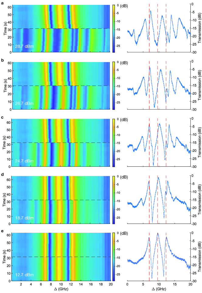
We characterize the effects of RF modulation on mode drift by applying RF modulation at GHz and recording a series of spectra on the VNA. After collecting several traces, we turn off modulation and record another series of traces. By recording the time stamp of each scan, we measure mode drifts in near real-time.
Figure S7 presents scans taken at various RF powers. The black dashed line indicates the first scan for which modulation is turned off in each set. The individual traces correspond to the last scan under RF modulation. We normalize these traces to the maximum amplitude of the modes before any modulation is applied (i.e., before taking data in Fig. S7e). Operating our EOM at the DC phase point, we approximate peaks in the spectra as mode locations. We track the center mode’s location and observe drift on the order of half of a linewidth under high-power modulation. After turning off RF modulation, the modes relax to their initial locations. There is an initial offset drift in the mode location at each RF power, which we believe occurs on a timescale shorter than the speed at which we extract data from the VNA.
This measurement scheme is useful for in situ mode characterization, as the mode behavior can be observed nearly independently of such effects as the optical power or the laser sweep rate (which changes intra-cavity optical power). The VNA/EOM sweeps are rapid and low-power, yielding an almost constant optical energy into the modes, and visualizing what appears to be steady-state mode behavior. This steady-state changes for different laser pump amplitudes, DC bias voltage, or RF power, but is independent of the VNA sweep rate or power applied to the EOM. We believe mode drift and distortion are functions of pump depletion and on-chip heating at high RF modulation powers.
S4 Detuning Effects
S3.1 Microwave Detuning
It is inefficient to drive the inter-band transitions with an RF tone that is detuned from the inter-band coupling rate (). Doing so shifts the phase condition required to achieve maximum isolation, and the converted sideband shape becomes asymmetric. This effect is exacerbated when there is disorder in the mode hybridization. In this case, one inter-band transition better matches the RF drive frequency than the other, leading to more efficient conversion at this transition. The amplitudes of the converted sidebands differ, altering the power-matching condition required for isolation.
We detune the microwave drive from the ideal value and observe changes in lineshape and fluctuations in the isolation parameter, as depicted in Fig. S8. These plots are measured for microwave drive amplitudes and frequencies as given in table S1.

S3.2 Laser Detuning and Isolation Bandwidth
Detuning the optical signal from the resonance location has a similar effect as RF detuning on the lineshapes and isolation parameters. There is disorder in the hybridization, evidenced by misalignment between the maximum isolation and the resonance condition. From coupled mode theory, we can predict the isolation bandwidth at the ideal power matching condition and , as given in the main text. For input and output frequencies detuned from the signal frequencies by , isolation parameters in the ideal system (i.e., no disorder in the mode hybridization) are given by:
| (14) |
The 3 dB isolation bandwidth (FWHM) is given by twice the linewidth of the intermediary mode in the indirect transition pathway. In practice, our modes have disorder and exhibit some drift with RF drive power. We observed isolation that remained within a few dB of maximum over hundreds of MHz.
S4 Optical Power in the Cavity
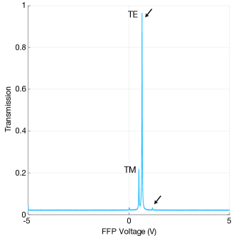
We characterize optical power in the three resonators. Following the procedure set out by Jiang et al. (2020b), we drive the EOM at various bias points, pass the output through a fiber Fabry-Perot filter (Micron Optics FFP), and record the transmission on a photodiode. The transmission is depicted in Fig. S9. By comparing the sideband and carrier amplitudes after subtracting the detector noise floor, we identify how much light is scattered into sidebands for given modulation frequencies. We fit the scattering efficiency over a few drive frequencies to interpolate how much light is scattered into sidebands at the frequencies used in this experiment. By measuring the input power to the device ( mW) and assuming equivalent coupling efficiency on the input and output of the device (), we determine that approximately uW ( uW and uW) of light propagates in the feed waveguide for signals at ( and ).
We use the input-output formalism presented in section S1.1 to determine the flux into the first racetrack coupled to the waveguide:
| (15) | ||||
| (16) | ||||
| (17) |
Substituting for the input flux, , in terms of optical power, we can solve for the circulating power in the first resonator:
| (18) |
In this expression and refers to input signal power at a signal frequency propagating in the waveguide. We can similarly solve the input-output relations to obtain expressions for the power circulating in the second and third resonators:
| (19) |
| (20) |
From equations 18,19,20, using the average fit parameters obtained in section S1, we obtain power in resonators 1,2, and 3 for various signal frequencies (table S2).
| Signal Frequency | Input Power (W) | Res. 1 (mW) | Res. 2 (mW) | Res. 3 (mW) |
|---|---|---|---|---|
| 5.07 | 77 | 187 | 111 | |
| 4.33 | 127 | 1.92 | 127 | |
| 3.59 | 72 | 123 | 52 |