Simulations of hybrid charge-sensing single-electron-transistors and CMOS circuits
Abstract
Single-electron transistors (SETs) have been extensively used as charge sensors in many areas such as quantum computations. In general, the signals of SETs are smaller than those of complementary metal-oxide semiconductor (CMOS) devices, and many amplifying circuits are required to enlarge these signals. Instead of amplifying a single small output, we theoretically consider the amplification of pairs of SETs, such that one of the SETs is used as a reference. We simulate the two-stage amplification process of SETs and CMOS devices using a conventional SPICE (Simulation Program with Integrated Circuit Emphasis) circuit simulator. Implementing the pairs of SETs into CMOS circuits makes the integration of SETs more feasible because of direct signal transfer from the SET to the CMOS circuits.
Single-electron transistors (SETs) have been intensively investigated owing to their advantages of low-power operation, which is desirable for application to logic and memory elements Grabert ; Likharev . Since Tucker’s proposal Tucker , many approaches have been developed to replace the elements in complementary metal-oxide semiconductor (CMOS) circuits Chen ; Tiwari ; Yano ; Mahapatra ; Inokawa ; Uchida . SETs were also investigated after they were directly embedded in CMOS circuits Yano ; Uchida2 ; Inokawa . Currently, conventional Si transistors are much smaller than SETs. SETs have attracted attention as charge sensors Field ; Berman ; Ionescu , which have been used for the readouts of silicon qubits Morello ; Gonzalez-Zalba ; Shaji , or as current standards Fujiwara ; Nishiguchi ; Fujiwara2 .
The SET consists of a small metallic island or a degenerated semiconductor island surrounded by a source and drain via tunneling junctions with low capacitances. The SET yields periodic outputs referred to as Coulomb oscillations, which vary as a function of the gate voltage, and the oscillation period corresponds to the change in the number of electrons in the island. The maximum signal change in an SET is the difference between the peak and the trough of the Coulomb oscillation. The SET current is sensitive to electric potential variations on the SET island Field . The standard readout process of a spin qubit (spin in localized states, such as a single impurity or quantum dot (QD)) is a spin-to-charge conversion, and the change in charge of the localized state is detected by the SET current Schoelkopf ; Lu ; Morello ; Gonzalez-Zalba .
There are many methods for the detection of charges, such as the use of radiofrequency SETs (rf-SETs) Schoelkopf ; Lu ; Gonzalez-Zalba and the direct measurement of the SET by a single GaAs amplifier Petersson ; Visscher . Inokawa et al showed that a Coulomb oscillation is effectively outputted by directly connecting the SET to an MOS field-effect transistor. They experimentally demonstrated multiple-valued logic by SETs operating at 27 K. The effectiveness of the series coupling of the SET with MOS transistors was also experimentally investigated by Uchida et al. Uchida2 . Scalable SET sensing systems require scalable circuits. However, previous SET sensors Morello ; Gonzalez-Zalba ; Shaji ; Fujiwara ; Nishiguchi ; Fujiwara2 did not explicitly consider the array of SETs as part of CMOS circuits.
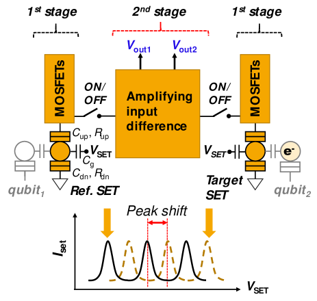
In this study, we theoretically consider a scalable detection circuit based on the implementation of many SETs in CMOS circuits. Our basic concept of the amplification of the SET signals consists of two stages, as shown in Fig. 1. The first amplification stage of the process is conducted by direct connection of the SET to pMOS transistors. In the second stage, we introduce a reference and a target SET and amplify the difference between two SETs using standard amplifier circuits, such as the differential amplifier (DA) circuits, and the static random-access memory (SRAM) cells.
For smooth connection to the digital circuits, the output of the sensing circuit should be a digital signal (either a ”0” or a ”1”). For this purpose, it is better to compare the relative output of the target SET with that of the reference SET. In our application of the SRAM cell, the relative voltage difference between the target SET and the reference SET is found to be quickly latched to ”0” or ”1.” This is in contrast to the measurements in Refs. Morello ; Gonzalez-Zalba ; Shaji , wherein the results were obtained after the analysis of a series of time-dependent SET currents. Our CMOS circuits are assumed to be close to the SETs. In addition, the target and the reference SETs are chosen by switching on the wordline transistors between the pairs of SETs and amplifiers. Then, the circuit using the pairs of SETs becomes more compact than the amplifying circuit of a single SET. Accordingly, our proposal is suitable for an array of sensing SETs.
In this study, we implement the current characteristics of the orthodox theory of the SET Amman into the SPICE (Simulation Program with Integrated Circuit Emphasis) circuit simulator based on the BSIM4 (Berkeley Short-channel transistor Model, level=54) by using the standard modeling language of the Verilog-A. We considered two types of SETs one of which is operated at low (4.2 K), and the other is operated at high temperatures (-30∘C). At low temperatures, such as 4.2 K, the threshold voltage of the MOS transistors becomes higher because of the incomplete ionizations. Many studies regarding cryo-CMOS Green ; Gaensslen ; Beckers ; Dijk have been conducted to determine the model parameters at low temperatures. However, the general compact model is not available for such low temperature. In addition, the basic CMOS operations are basically the same as that at room temperature (RT). Thus, we applied the CMOS parameters that are available in the conventional SPICE models to the CMOS parts for both types of the SETs. In the following, circuit calculations are mainly conducted at C, which is in the range of the conventional models.
We consider CMOSs with gate lengths of 90 nm and 65 nm, whose drain voltages are 1.2 V and 1.0 V, respectively. We also consider the effects of small variations in the SETs and CMOS transistors. The purpose of the comparison of pairs of SETs is to detect the changes in the Coulomb oscillations of the target SET. Thus, given that the voltage difference between the peak and trough currents of the Coulomb oscillations can be distinguished, we will be able to detect the changes of the target SET even if there are variations in the devices.
| Capacitance(aF) | Resistance() | Temp(K) | (meV) | ||||
|---|---|---|---|---|---|---|---|
| SET | |||||||
| LT-SET | 1 | 10 | 2 | 100k | 1M | 4.2 | 6.16 |
| LT-SET | 1.1 | 0.9 | 2.2 | 110k | 0.9M | 4.2 | 6.51 |
| RT-SET | 0.1 | 0.5 | 0.5 | 100k | 500k | 243 | 72.8 |
| RT-SET | 0.11 | 0.45 | 0.45 | 110k | 450k | 243 | 79.3 |

Herein, we consider four SETs, as listed in Table I. The LT-SET (target) and LT-SET (reference) are operated at 4.2 K, and RT-SET and RT-SET can operate at -30∘C. The parameters of the LT-SET (RT-SET) exhibit 10% variations compared with those of the LT-SET (RT-SET). The calculated current–voltage characteristics (-) are listed in the appendix. The charging energy is given by . The magnitude between the peak and trough currents is on the order of pA, and its voltage change estimated by pA 25.9 k 25.9 V is very small (25.9 k is a quantum resistance Grabert ). On the other hand, the variations in the threshold voltage of conventional CMOSs are generally on the order of millivolts. Therefore, we need to amplify the SET outputs before connecting the SETs to conventional CMOS circuits.
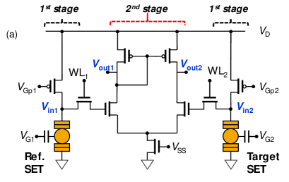
We start from the first amplification stage in which the SET is directly connected to the CMOS transistors, as shown in Fig. 2(a). By a series connection, the low SET current value increases with CMOS Inokawa . Figure 2(b) shows that the amplification of the SET signal becomes prominent at V. The distortions of the waveforms compared with the original Coulomb oscillations originate from the nonlinearity of the - characteristics of the pMOS transistors. We analyze the amplification mechanism based on the standard long-channel model Taur . The - of CMOS transistors depends on the triode region and the saturation region . At present, amplification is observed in 1.05 V V (saturation region). We did not observe a sufficiently large amplification in the triode region. The SET current under large source-drain voltage is approximately described by (see appendix). More explicitly we assume that . Thus, we can write the - characteristics in the saturation region; further, the SET given by
| (1) | |||||
| (2) |
The solution of these equations is given by
| (3) |
where . Because , the SET output is enhanced by . Note that is conspicuous in both the 90 nm and 65 nm pMOS transistors (see appendix), and we can see that the output voltage oscillates around 10 mV in Fig. 2(b).
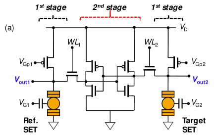
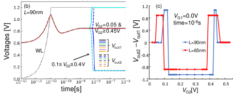
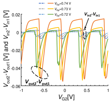
The second-stage amplification is conducted using standard amplifier circuits. Figure 3 shows the results obtained from a basic DA circuit. Note that the gate voltages and represent the shifted electrical potential by the additional sensing QD in Fig. 1. Conventional DAs amplify two inputs with opposite phases. In the case of SETs, two different phases of Coulomb oscillations are input. We consider that the two SET signals possessing different current peaks mimic the two input signals of the conventional DA with different phases. In Figs. 3(b), we show the results for the output voltage difference of for a fixed . The voltage difference increases by approximately 40 mV for nm (the results for nm are shown in the appendix), and can be detected by conventional CMOS amplifier circuits (the following circuits after and are not shown). This enhancement of the Coulomb oscillations is the result of the two-stage amplification of SET signals.
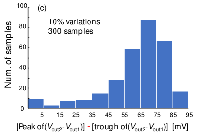
The magnitude of the enhancement of the Coulomb oscillation in Fig 3(b) changes depending on the threshold voltage variations of the eight MOS transistors. In Fig.3(c), we provide the distribution of the difference in the peak and trough of obtained through over 300 Monte Carlo simulations of the threshold variations with LT-SET and LT-SET at and V. The number of small amplitudes of ( 5 meV) is nine out of 300 samples. Small amplitudes of can be avoided by applying different voltages such as and on each part of the DA.
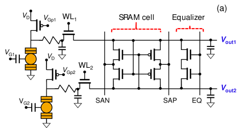
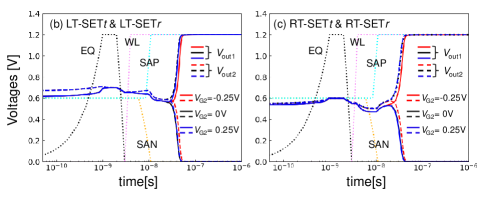
We now consider the application of the standard SRAM cell containing six MOS transistors Seevinck to detect a pair of SETs, as shown in Fig. 4(a). Figure 4(b) shows the simulation results of the time-dependent SRAM cell outputs and of the two LT-SETs. We can see that for V, but for VV for = 90 nm devices. This implies that the shift in the electric potential of the sensing QD from V to V changes the electric potential of the target SET island, resulting in a change in the relative magnitude between and . Figure 4(c) replots in Fig. 4(b) as a function of with the results for 65 nm at time s. Thus, we can detect the change in the target SET represented by by measuring the relative outputs of the SRAM cell. Herein, the initial voltage at the SRAM cell input is set to , and stray capacitances of 0.2 pF are included at the input nodes of the SRAM cell (Figures not shown). As the stray capacitance increases, the time to split increases.
In general, SRAM cells undergo initial threshold voltage variations PUF , and we have to consider these variations in the MOS transistors as well as the two SETs. Here, we extend the SRAM cell circuit to a dynamic random-access memory (DRAM)-like structure DRAM1 ; DRAM2 in Fig. 5(a), where it is considered that the equalizer circuit mitigates the voltage difference of the wordlines between the two SETs. Figures 5(b)(c) show two types of readouts for the two types of SETs. The equalizer voltage is switched on at 1 ns and stopped after 2 ns. The SAN and SAP voltages are switched on after the equalizer at ns and ns. The wordlines are switched on at 4 ns. We can see that the change in the gate voltage , which corresponds to the existence of the charge sensor QD, causes the outputs and to change from to .
In a realistic situation, it is possible that the temperature changes. Therefore, we also calculated the temperature dependence of the amplifier response. It is desirable that the relative magnitude of to does not change even when the operating temperature changes. The temperature dependencies of the characteristics of the DA (Fig. 3) and DRAM (Fig. 5) are robust against temperature changes as long as the temperature change is sufficiently small on the order of several tens of degrees (see appendix).
Considering that there are variations in SETs and MOS transistors, we may have to check and record the basic characteristics of each device at the first calibration stage of the chip. The – characteristics of each SET should be clarified before using the charge-sensing SET. This information is stored in the extra SRAM or other memories, and becomes the overhead of the system. An effective method for determining the optimal biases automatically is a future issue. It is possible that the applied voltages destroy the SET charge states. However, herein, we neglected the effects of the backaction from the CMOS circuits. Hence, the assessment of the backaction remains a future issue.
In conclusion, we proposed two-stage amplification circuits for SETs. Based on serial connections with MOS transistors and a comparison with the reference SET, we numerically show that the readout of the charge-sensing SET is greatly enhanced. We also considered the effects of variations in the MOS transistors and SETs, and show that as long as the variations are small, the two SETs can be compared effectively.
DATA AVAILABILITY
The data that supports the findings of this study are available within the article.
Acknowledgements.
We are grateful to T. Mori and H. Fuketa for the fruitful discussions. We are also grateful to Y. Yamamoto for his technical support in using SmartSpice. This work was partly supported by MEXT Quantum Leap Flagship Program (MEXT Q-LEAP) Grant Number JPMXS0118069228, Japan.Appendix A SET characteristics determined by the orthodox theory
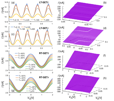
Figure 6 shows the current-gate voltage characteristics of the four SETs used in the main text, calculated based on the orthodox theory Amman . The Coulomb staircase becomes clearer for a large asymmetry between the two tunnel junctions; however, the amplitude of the oscillation becomes smaller. Therefore, we consider the case of a smaller asymmetry. The wide-range view of the current–voltage () characteristics o f the SET shown in Figs. 6(b)(d)(f)(h) enables the approximation of of Eq.(2) in the main text.
Appendix B Additional results for the transistors and amplification circuits
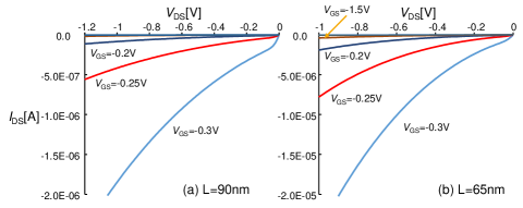
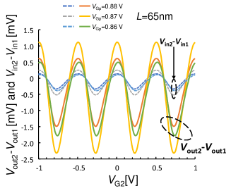
Figure 7 shows the basic - characteristics of the pMOS transistors used herein (Berkeley short-channel transistor model BSIM-4), and Fig. 8 shows the characteristics of the DA circuits of Fig. 3 (b) for = 65 nm. Although amplification is not observed in the triode region, herein, we show that amplification can be expected even in the triode region. In the triode region, Eq. (1) is replaced by
| (4) |
where and are the channel length modulation coefficients (, , , and are the length, width, gate capacitance and mobility of the pMOS, respectively). The solution to the equations is given by
| (5) |
where . Eq. (5) shows that the SET output changes the rate of . When we take m2/(Vs), with and nm for 90 nm and m, we have AV-2 and V-1 for M. Then the change rate mV. Whether the triode region or the saturation region is better for the amplification depends on the current characteristics of the MOS transistors.
Appendix C Temperature dependence
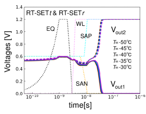
We calculated the temperature dependence of the amplifier response. It is desirable that the relative magnitude of to does not change as long as the operating temperature changes in the range of approximately -50C. Figures 9 and 10 show the temperature dependence of the characteristics of the DA (Fig. 3), and DRAM (Fig. 5). For example, depending on the value of , we can observe the relative change in the magnitude between and . We also observe that even when there are variations, the two SETs can be differentiated by changing the gate voltage or . The strength to the change of temperature depends on each operation region.

Appendix D Detection by cross-coupled circuit
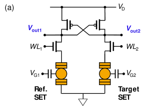
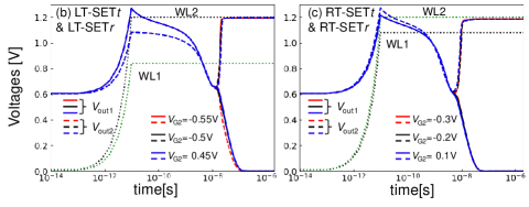
Figure 11(a) shows our other proposal based on the cross-coupled type. In this case, two SETs are series-connected to cross-coupled MOS transistors, where the changes in the SET signals are directly transferred to the MOS transistors. Herein, the 10% variations between the SETs and among the MOS transistors are considered. To observe the change in to the fixed , we have to adjust the wordline voltages. In Figs. 11(b) and 11(c), the wordline voltage of the left SET is reduced to V, and V, respectively. In Fig. 11(b)((c)), becomes higher than between V and V ( V and V). When there are no variations, the left and right hand circuits are exactly the same, and and are clearly split depending on the gate voltages of the two SETs. Temperature changes are not observed, similar to the case with the SRAMs mentioned above (Figures not shown).
References
- (1) H. Grabert and M. H. Devoret, ”Single Charge Tunneling: Coulomb Blockade Phenomena In Nanostructures” (Nato Science Series B:)(Springer, New York, 1992).
- (2) K. K. Likharev, Proc. IEEE, 87, 606 (1999).
- (3) J. R. Tucker, J. Appl. Phys. 72, 4399 (1992).
- (4) R. H. Chen, A. N. Korotkov, and K. K. Likharev, Appl. Phys. Lett. 68, 1954 (1996).
- (5) S. Tiwari et al., Appl. Phys. Lett. 68, 1377 (1996).
- (6) K. Uchida et al., Jpn. J. Appl. Phys. 38, 4027 (1999).
- (7) S. Mahapatra and A. M. Ionescu, 4th IEEE Conference on Nanotechnology p.287 (2004).
- (8) H. Inokawa, A. Fujiwara and Y. Takahashi, IEEE Trans. Electron Devices, 50, 462 (2003).
- (9) K. Yano et al., 1999 IEEE International Electron Devices Meeting 87, 633 (1999).
- (10) K. Uchida et al., Digest of ISSCC 2002, 206 (2002).
- (11) M. Field, C. G. Smith, M. Pepper, D. A. Ritchie, J. E. F. Frost, G. A. C. Jones, and D. G. Hasko, Phys. Rev. Lett. 70 1311 (1993).
- (12) D. Berman J. Vac. Sci & Tech. B 15, 2844 (1997)
- (13) A. M. Ionescu, M. J. Declercq, S. Mahapatra, K. Banerjee and J. Gautier, Proceedings 2002 Design Automation Conference pp. 88-93 (2002).
- (14) A. Morello,et al., Nature 467, 687 (2010).
- (15) Gonzalez-Zalba et al., Nat Commun 6, 6084 (2015).
- (16) N. Shaji et al., Nature Phys 4, 540 (2008).
- (17) A. Fujiwara, et al., Appl. Phys. Lett. 88, 053121 (2006).
- (18) K. Nishiguchi and A. Fujiwara, 2007 IEEE International Electron Devices Meeting, 791 (2007).
- (19) S. P. Giblin et al., Metrologia 57, 025013 (2020).
- (20) R. J. Schoelkopf et al., Science 280, 1238 (1998).
- (21) W. Lu, Z. Ji, L. Pfeiffer, K.W. West, and A.J. Rimberg, Nature 423, 422 (2003).
- (22) J. Petersson et al., Phys. Rev. B 53, 13272 (1996).
- (23) E. H. Visscher et al., Appl. Phys. Lett. 68, 2014 (1996).
- (24) M. Amman, R. Wilkins, E. Ben-Jacob, P. D. Maker, and R. C. Jaklevic, Phys. Rev. B 43, 1146 (1991).
- (25) R. R. Green, Rev. Sci. Instrum., 39, 1495 (1968).
- (26) F. H. Gaensslen, V. L. Rideout, E. J. Walker and J. J. Walker, IEEE Trans. Electron Devices, 24, 218 (1977).
- (27) A. Beckers, F. Jazaeri, A. Ruffino, C. Bruschini, A. Baschirotto and C. Enz, 2017 47th European Solid-State Device Research Conference (ESSDERC), p. 62, (2017).
- (28) J. van Dijk et al., 2020 IEEE Custom Integrated Circuits Conference (CICC), p. 1, (2020).
- (29) Y. Taur and T. H. Ning, ”Fundamentals of Modern VLSI Devices” (Cambridge University Press, 1998).
- (30) E. Seevinck, F. J. List and J. Lohstroh, IEEE J. Solid-State Circuits, 22, 748 (1987).
- (31) D. E. Holcomb et al.,IEEE Trans. Comput. 58, 1198 (2009).
- (32) B. Keeth and R. J. Baker, ”DRAM Circuit Design: A Tutorial” (John Wiley & Sons, 2001).
- (33) B. Jacob, D. Wang, and S. Ng, ”Memory Systems: Cache, DRAM, Disk” (Morgan Kaufmann; 1st edition, Amserdam 2007).