Genetic-algorithm-aided ultra-broadband perfect absorbers using plasmonic metamaterials
Abstract
Complete absorption of electromagnetic waves is paramount in today’s applications, ranging from photovoltaics to cross-talk prevention into sensitive devices. In this context, we use a genetic algorithm (GA) strategy to optimize absorption properties of periodic arrays of truncated square-based pyramids made of alternating stacks of metal/dielectric layers. We target ultra-broadband quasi-perfect absorption of normally incident electromagnetic radiations in the visible and near-infrared ranges (wavelength comprised between 420 and 1600 nm). We compare the results one can obtain by considering one, two or three stacks of either Ni, Ti, Al, Cr, Ag, Cu, Au or W for the metal, and poly(methyl methacrylate) (PMMA) for the dielectric. More than configurations of geometrical parameters are explored and reduced to a few optimal ones. This extensive study shows that Ni/PMMA, Ti/PMMA, Cr/PMMA and W/PMMA provide high-quality solutions with an integrated absorptance higher than 99% over the considered wavelength range, when considering realistic implementation of these ultra-broadband perfect electromagnetic absorbers. Robustness of optimal solutions with respect to geometrical parameters is investigated and local absorption maps are provided. Moreover, we confirm that these optimal solutions maintain quasi-perfect broadband absorption properties over a broad angular range when changing the inclination of the incident radiation. The study also reveals that noble metals (Au, Ag, Cu) do not provide the highest performance for the present application.
keywords:
Ultra-broadband absorption, plasmonic metamaterials, genetic algorithmNamur]Laboratoire de Physique du Solide, University of Namur, Rue de Bruxelles 61, 5000 Namur, Belgium \altaffiliationThese authors contributed equally to this work. \alsoaffiliationJi Hua Laboratory, Island Ring South Street, Foshan, Guangdong 528000, P. R. China CSL]Centre Spatial de Liège, Avenue du Pré-Aily, 4031 Angleur, Belgium \alsoaffiliationFaculty of Aerospace Engineering, Delft University of Technology, Delft, 2629 HS, Netherlands Namur]Laboratoire de Physique du Solide, University of Namur, Rue de Bruxelles 61, 5000 Namur, Belgium Namur]Laboratoire de Physique du Solide, University of Namur, Rue de Bruxelles 61, 5000 Namur, Belgium \alsoaffiliationCentre Spatial de Liège, Avenue du Pré-Aily, 4031 Angleur, Belgium \alsoaffiliationJohn A. Paulson School of Engineering and Applied Sciences, Harvard University, 9 Oxford Street, Cambridge, MA 02138, United States of America \altaffiliationThese authors contributed equally to this work. \abbreviationsIR,NMR,UV
1 Introduction
Since its theoretical introduction in 1860 by G. Kirchhoff, the black body concept played a seminal role in the history of quantum mechanics and modern physics.1 It originally referred to an idealized physical body of infinitely small thickness, that completely absorbs all incident rays, and neither reflects nor transmits any.2 The modern acceptance of the term does not include the infinitely small thickness anymore but still preserves the requirement to absorb all incident electromagnetic radiation regardless of the wavelength, the polarization or the angle of incidence of the incoming radiation. First experimental realizations of black bodies at the end of the 19th century/ dawn of the 20th century consisted of metallic boxes with its interior walls blackened by mixed chromium, nickel and cobalt oxides. 3, 4, 5 The quest for a Perfect Electromagnetic Absorber (PEA), i.e. the materialization of the idealized black body, continued over the years for example due to the recent need of efficient solar energy harnessing or camouflage solutions, the development of photothermal detectors or in order to prevent crosstalk in nanoscale opto-electronics and quantum technologies.6, 7 Among efficient solutions, carbon black and carbon nanotubes materials provide ultra-broadband PEA with 98-99 absorption from UV to far infrared8 while nickel-phosphorus alloy reach 96 % on the range.9
At the dawn of the present century, metamaterials and plasmonic materials provided new opportunities in order to mold the flow of light at the nanoscale and drastically enhance light-matter interactions 10, 11, 12, 13. Negative refraction, cloaking, superlensing, near-zero refractive index, surface enhanced Raman scattering, high energy concentrations at metal-dielectric interfaces are some examples of current interest among those hot topics in photonics.14, 15, 16 Nevertheless, losses due to metallic components are an important drawback limiting current applications.17 This drawback was turned into an advantage by Landy et al. who designed the first metamaterial PEA by using metallic resonators operating at a single wavelength.18 The metamaterial approach was successfully applied during the last decade in order to tame the black body radiation and provide efficient PEA over a broad range of frequencies.19, 20, 21, 22, 23, 24, 25, 26, 27, 28, 29, 30, 31, 32, 33, 34 Some proposed theoretical structures are nevertheless facing some technological difficulties due to the current limitations in resolution and complexity of the structures, especially in the visible range. The field of plasmonic metamaterials PEA is now mature enough to enter a novel phase of in silico modeling in order to develop more realistic PEA,35, 36, 37 while preserving the ultra-broadband character of the PEA as well as its low angular dependency.
Here, we report on ultra-broadband metamaterial PEA using periodic stacks of square metal/dielectric layers arranged in a pyramidal way (see Fig. 1). We investigate among twenty-four possible PEA which are realistic from an experimental point of view and based on eight common metals arranged either in one, two or three stacks of metal/dielectric layers. The fact that the number of layers is limited to a few ones, while preserving the performances, is attractive in view of the tradeoff between fabrication complexity and broad absorption properties. It provides realistic perspectives for device fabrication with current technology. No less than configurations are explored by varying different experimental parameters such as the lateral size of the metal/dielectric layers, the thickness of the dielectric layer or the lateral periodicity between different individual structures. The search for the optimal configuration, i.e. the PEA with the largest absoptance of electromagnetic (EM) radiations over the visible to mid-infrared (MIR) range, is realized using a Genetic Algorithm (GA) strategy. Optimal configurations are reported as well as their absorptance spectra. Moreover, fields maps and angular dependency of the optimal PEA are discussed. The latter is primordial for several applications of black coatings such as cross-talk prevention in qubits.6, 7 or stray light reduction38, 39.
2 Design
Energy conservation imposes that reflectance , transmittance and absorptance are related through
| (1) |
with being the wavelength of the incident EM radiation and the angle of incidence. Maximizing absorption requires suppressing both transmission and reflection at the same time. The PEA can be made opaque, i.e. no transmission, by adding a metallic layer over the substrate. In order to lower the reflection, the PEA needs to be impedance matched. Surface corrugations in a tapered way provide this gradual transition between the refractive indices of both incidence and substrate media. This anti-reflection strategy is well-known both in Nature or in transparent coatings 40, 41. The previous approach leads to suppressed transmission () and drastically reduced reflection (). To minimize reflection and fully absorb the incident radiation in order to obtain a PEA, the energy transported by the radiation has to be dissipated through the excitation of eigenmodes of the structure. This can be done for example by exciting localized surface plasmons (LSP) at the interfaces of metal/dielectric square resonators 42, 43, 44, 45. The wavelength associated with these plasmonic resonances is proportional to the lateral dimensions of the metallic layers, conferring the desired broadband character once metallic resonators of varied sizes are stacked. Following this approach, truncated square-based pyramids made of twenty stacks of Au/Ge layers lead to an integrated absorptance of 98% of normally incident radiations over a 0.2-5.8 m wavelength range46, 47. However, fabrication of such elaborated structures, with nanometer resolution and high number of layers is currently too demanding in terms of time and resources.
There is thus a need for simplified structures to reach ultra-broadband PEA that are tractable experimentally. Therefore, we consider here a simpler PEA consisting of one, two or three stacks of metal/dielectric layers (see Fig. 1).35, 36. We set the thickness of all metal layers within the pyramid stack to 15 nm,46 which is smaller than the skin depth of the metals considered over the targetted radiation wavelength range, i.e. from 420 to 1600 nm here. It allows therefore a coupling between the surface plasmons at the two sides of each metallic layer. Moreover, we consider poly(methyl methacrylate) (PMMA) as dielectric 48, 35, 36. PMMA can be easily deposited using spin-coating techniques and its thickness can be simply varied by changing PMMA/solvent relative concentration in solution, or spinning speed for example.
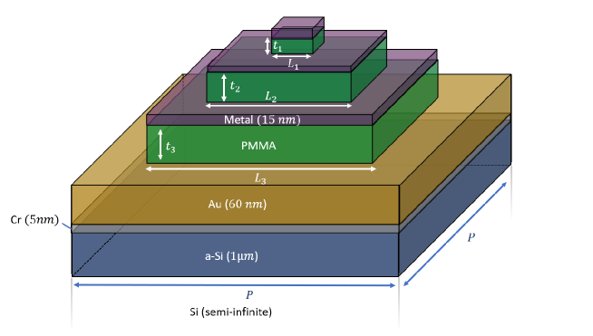 |
A vast range of metals are considered in the present study, namely Ni, Ti, Al, Cr, Ag, Cu, Au or W.49, 50, 51, 52 Those metals correspond to widely used materials in current nanophotonics applications, and are readily deposited to form few nm-thick films through physical deposition techniques. The thickness of each dielectric layer and the lateral dimension of each metal/dielectric stack are adjustable parameters in the present GA-aided approach. The lateral periodicity of the system also remains an adjustable parameter. This relaxation of the PEA dimensions, as compared with previous studies46 where thickness was the same for all metallic layers and for all dielectric layers, provides the extra degrees of freedom that are necessary to maintain high performances while reducing the number of metallic layers.
The role of these different parameters can be understood as follows. The lateral dimensions of the metallic resonators essentially control the plasmonic resonances of the system. The thicknesses of the dielectric layers control the vertical coupling between these resonators while the periodicity finally controls the lateral coupling between the pyramids 46. The detailed variation range of these parameters are provided in SI. Furthermore, the PEA stands on a flat 60 nm-thick gold layer that blocks the transmission of the considered incident radiations and reflects any EM radiation not absorbed in the pyramids. This gold layer stands on a 5-nm thick chromium (Cr) adhesion layer followed by a 1 µm-thick amorphous silicon (a-Si) layer. We consider finally a semi-infinite Si substrate (). This choice of a silicon substrate has no impact on our results since no radiation will actually reach this region.
3 Optimization schemes
For a system made of stacks of metal/dielectric layers, we consequently have a total of parameters to consider (i.e., , and for ). Different methods are used in optics to determine optimal parameter combinations. The systematic evaluation of a whole grid of possible parameter combinations is generally limited to two or three parameters. Local optimization methods such as the (quasi-)Newton method or gradient descent are more efficient in terms of the required number of function evaluations.53 They converge however generally to the first local optimum encountered. Global optimization methods are preferable in this respect since they provide a wider exploration of the parameter space, which can eventually lead to higher-quality solutions (ideally the best-possible solution). Genetic Algorithms (GA),54, 55, 56 Particle Swarm Optimization (PSO)57, 58, 59 and Ant Colony Optimization (ACO)60 are popular global optimization methods that rely on a collective exploration of the parameter space. The population dynamics of these algorithms is inspired by the principles of natural selection for GA, birds flocks dynamics for PSO or pheromone-guided exploration for ACO. These methods can easily escape local optima and find higher-quality solutions. They do not require the calculation of gradients. They are intrinsically suited to a parallel computing, since the fitness of each individual in the population can be evaluated independently. Machine Learning (ML) techniques such as deep neural networks or autoencoders can help the search by learning representations of the function to optimize61.
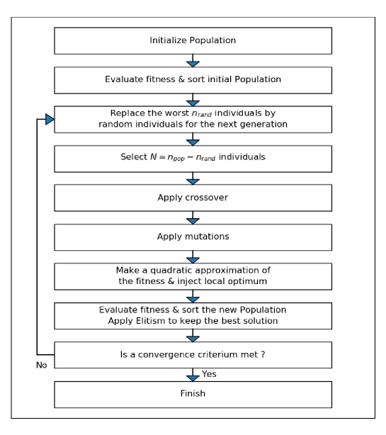 |
We use in this work a home-made genetic algorithm (see workflow in Fig. 2 and the Supplementary Material for a detailed description) to address this optimization problem and establish realistic structures that consist of only one, two or three stacks of metal/dielectric layers. We consider in particular poly(methyl methacrylate) (PMMA) for the dielectric and either Ni, Ti, Cr, Al, Ag, Cu, Au or W for the metal (eight possible materials). This makes a total of 24=38 structures (1 to 3 layers, 8 metals) that are optimized with the objective to maximize the absorption of normally incident radiations with wavelengths comprised between 420 and 1600 nm.
The objective function to be maximized (also called fitness or figure of merit) will be the integrated absorptance for normally incident radiations with wavelengths comprised between 420 and 1600 nm. It is formally defined by , where refers to the absorptance of normally incident radiations at the wavelength , =420 nm and =1600 nm. This is the quantity that the Genetic Algorithm seeks at maximizing by exploring the geometrical parameters of the structure considered. It relies on an homemade Rigorous Coupled Waves Analysis (RCWA) code that solves Maxwell’s equations exactly for stratified periodic systems.62, 41 A plane wave (PW) expansion of the electric permittivity of the PEA is made, in which the number of Fourier components is the key parameter to insure numerical convergence.
4 Results and discussion
Once the GA started, one can follow generation after generation the fitness of the best individual in the population as well as the mean fitness in the population. The best fitness usually increases rapidly in the first generations as better solutions are rapidly detected. Progress becomes typically slower after these first generations as the algorithm must either escape a local optimum to detect a radically different solution (exploration) or refine the best solution found so far to finalize the optimization (exploitation). A good optimization algorithm must actually find a sound balance between these two aspects. The mean fitness of the population follows the best fitness, to a degree that depends on the convergence of the population to the best individual, convergence measured by the genetic similarity defined in SM. Fig. 3 shows the best fitness and the mean fitness achieved in the first 80 generations, when optimizing stacks of W/PMMA. All optimizations are actually carried out by using plane waves in the RCWA simulations. The figure also shows the absorptance spectrum for the best solutions found by the genetic algorithm after 0, 5, 10, 18, 233 and 339 generations. High-quality solutions are established rapidly by the GA in the first generations ( at generation 0, 98.8% at generation 5, 99.0% at generation 10 and 99.3% at generation 18). Qualitative improvements become then slower. The final solution (=99.4%) is found after 339 generations in this case.
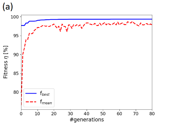
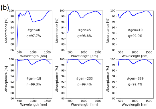
Fig. 4 shows the best fitness (integrated absorptance ) achieved for the different structures considered. These results correspond to , 2 and 3 stacks of metal/dielectric layers and the eight different metals considered in this study. They correspond to the systems actually optimized by the Genetic Algorithm (the optimization relies on RCWA calculations with plane waves; the final solutions are confirmed by considering plane waves). This extensive study reveals that Ni, W, Cr or Ti represent the best materials for this application. It is noticeable that integrated absorptance values above 86.1% are achieved for the optimized structures that correspond to these four metals. The best structures, which consist of stacks of Ni, W, Cr or Ti/PMMA layers, have all an integrated absorptance above 99%. Those results are, to the best of our knowledge, the best PEA proposed in recent literature over such an extended wavelength range in the visible and NIR. The geometrical parameters and the figure of merit obtained for the four best metals selected (Ni, W, Cr and Ti) are given in Table 1. The results that correspond to the other four metals (Al, Cu, Au and Ag) are given in Table 2. They will be discarded for this PEA application, essentially because of a lack of robustness of these solutions within the parameter space, i.e. sensitivity to experimental deviations, in addition to lower integrated absorptance values. It should be noted that three out of those four less convincing are noble metals (Cu, Au, Ag) and are usually considered as low-loss metals for plasmonic applications.17, 63 Considering that the choice of noble metals (Au, Ag, Cu) impacts on fabrication costs, it is interesting to note that they do not provide the highest performance for the present application.

Ni / PMMA (nm) (nm) (nm) (nm) (nm) (nm) (nm) stack 201 117 - - - - 286 95.0% 93.8% stacks 132 123 227 107 - - 287 99.4% 99.0% stacks 149 131 268 124 369 101 412 99.8% 99.3%
W / PMMA (nm) (nm) (nm) (nm) (nm) (nm) (nm) stack 250 115 - - - - 333 85.8% 86.1% stacks 222 127 368 119 - - 419 98.0% 98.0% stacks 152 117 266 122 379 125 419 99.4% 99.2%
Cr / PMMA (nm) (nm) (nm) (nm) (nm) (nm) (nm) stack 314 124 - - - - 419 88.8% 88.7% stacks 192 121 332 127 - - 369 98.5% 98.5% stacks 151 120 277 127 427 123 467 99.4% 99.1%
Ti / PMMA (nm) (nm) (nm) (nm) (nm) (nm) (nm) stack 368 134 - - - - 491 89.3% 88.9% stacks 175 117 306 127 - - 336 98.6% 98.5% stacks 161 125 302 126 451 113 491 99.4% 99.0%
Al / PMMA (nm) (nm) (nm) (nm) (nm) (nm) (nm) stack 221 151 - - - - 491 89.2% 63.8% stacks 187 108 263 58 - - 415 97.9% 81.0% stacks 129 112 208 110 294 97 465 98.7% 83.6%
Cu / PMMA (nm) (nm) (nm) (nm) (nm) (nm) (nm) stack 149 112 - - - - 230 80.9% 55.2% stacks 188 127 283 120 - - 447 89.1% 75.8% stacks 119 145 211 132 299 111 365 95.5% 77.5%
Au / PMMA (nm) (nm) (nm) (nm) (nm) (nm) (nm) stack 196 160 - - - - 416 68.5% 52.5% stacks 158 152 267 89 - - 326 85.5% 65.1% stacks 172 79 202 110 335 100 409 91.2% 70.4%
Ag / PMMA (nm) (nm) (nm) (nm) (nm) (nm) (nm) stack 152 112 - - - - 235 43.9% 35.8% stacks 179 144 303 108 - - 369 57.1% 42.9% stacks 101 151 193 155 268 110 330 66.1% 46.4%
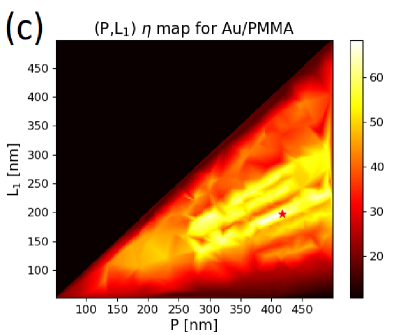
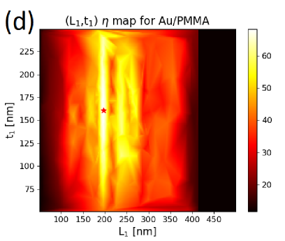
High-quality solutions must actually meet two requirements in order to be easily implemented in real devices: (i) to provide the highest possible integrated absorptance , but also (ii) to be robust with respect to slight variations of the geometrical parameters (compatibility with fabrication tolerances). We ideally want to find a broad optimum rather than a sharp one. When running the GA to find optimal geometrical parameters, it is possible to interpolate the data collected by the algorithm and establish maps of the fitness in 2-D planes that cross the -dimension point finally established by the GA. These maps reveal the robustness of the final solution (i.e., its stability with respect to slight variations of the geometrical parameters). An example is given in Fig. 5, where we compare the maps obtained when optimizing stack of Ni/PMMA (broad optimum - Fig. 5(a)-(b-) and stack of Au/PMMA (sharp optimum - Fig. 5(c)-(d)). These maps reveal that the solution found for Ni/PMMA is actually robust for practical applications, while the solution found for Au/PMMA is too sensitive. For =1 stack of Ni/PMMA, , and have indeed a domain of variation of 82 nm, 51 nm and 71 nm respectively around the optimum (domain associated with ). For =1 stack of Au/PMMA, this domain is reduced to 21 nm, 10 nm and 91 nm respectively. The lateral dimension is the most sensitive parameter in this case. All solutions presented in Table 1 were checked for their robustness, based on the inspection of the fitness maps established by the GA. They appeared to correspond to broad optima suitable for practical applications. On the contrary, the solutions presented in Table 2 were discarded because they actually correspond to sharp optima.
 |
 |
 |
 |
A quality check of the reliability of the presented solutions is performed by increasing the plane wave number to (see Table 1 and 2 and extended discussion in SM). This quality check allows us to further confirm the stability of our results: while increasing the plane wave number, good solutions (Table 1 - Ni;W;Cr;Ti) are stable regarding the parameter (deviation of limited to 1.2%, when comparing 1111 and 2121 PW), while less optimal ones (Table 2 - Al;Cu;Au;Ag) are much less stable (deviation of between 8.1% and 25.7%, when comparing 1111 and 2121 PW).
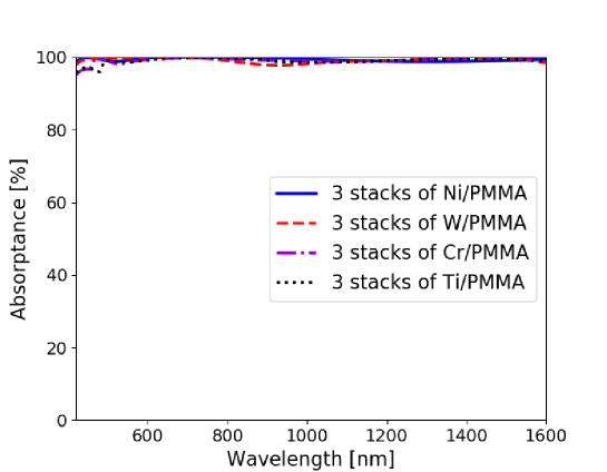
Fig. 6 represents the absorptance spectrum obtained for normally incident radiations with the four best structures identified in this work ( stacks of Ni/PMMA, W/PMMA, Cr/PMMA or Ti/PMMA). These structures provide respectively an integrated absorptance of 99.3%, 99.2%, 99.1% and 99.0% (results for RCWA calculations using 2121 plane waves). These results are amongst the best reported so far in the literature and confirm that the initial goal of designing an ultra-broadband PEA in the visible-NIR range is met. The challenge of fabricating such PEA is mitigated by the small number of layers and the selection of metals that are better alternatives to noble metals. Moreover, the proposed PEA are robust with respect to fabrication tolerances.
4.1 Plasmonic absorber characteristics
In order to better describe the physics of those PEA, we will focus from now on only on the best structure identified in this work, i.e. the one made of stacks of Ni/PMMA. It provides an integrated absorptance of 99.3%. As shown above, the solution is robust with respect to deviations of the geometrical parameters (broad optimum), as confirmed by 2-D maps of the fitness around the optimum and the comparison between the results obtained with 1111 and 2121 plane waves.
We can calculate the Poynting vector , where and refer here to the complex-number representation of the electric and magnetic fields, in order to show the energy flow through the structure. Moreover, we can determine the local absorption inside the PEA. Based on the method developed by Brenner,64 the absorbed power in a volume can be estimated by
| (2) |
with the local complex electric permittivity. By normalizing the absorbed power to the incident power , one obtains the local absorptance .
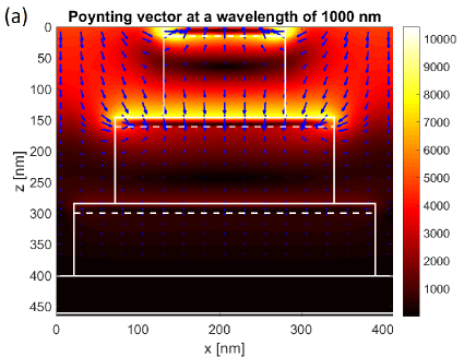
These calculations provide additional physical insight by showing in which parts of the structure the incident radiations are absorbed. An example is provided in Fig.7 for a normally incident radiation at a wavelength of 1000 nm. These results show that this radiation is essentially absorbed in the second metallic layer (25.9% of the incident radiation is absorbed in the top metallic layer, 50.3% in the central metallic layer and 23.3% in the bottom metallic layer). This is totally consistent with our previous work showing that the lower (upper) part of the pyramid absorbs higher (lower) wavelength 46, as predicted by the variation of LSP with the size of the resonators.
 |
 |
The results presented so far concerned the absorption of normally incident radiations. However, in many applications such as stray light mitigation, the PEA should be stable from an angular point of view. Therefore, we check how the integrated absorptance for stacks of Ni/PMMA depends on the polar and azimuthal angles ( and ) of the incident radiation. These results are presented in Fig. 8. The left part of this figure provides a complete 2-D map of the integrated absorptance with respect to the polar and azimuthal angles of the incident radiation. This map is actually generated by a cubic interpolation of data computed for only 73 points (blue points in the representation). The right part of this figure shows an horizontal section ( and ) for incident radiations that are either polarized (TE), polarized (TM) or unpolarized ((TE+TM)). These results show that the integrated absorptance remains quasi-perfect over a broad angular domain ( for ). This makes the proposed solution for a broadband quasi-perfect absorber made of three stacks of Ni/PMMA extremely robust for practical applications also from an angular point of view. Fig. 9 finally shows the horizontal profiles achieved when considering stacks of Ni/PMMA, W/PMMA, Cr/PMMA or Ti/PMMA, i.e. for the four best solutions identified in this work, in the case of an unpolarized incident radiation. This figure confirms the exceptional robustness of these best four solutions with respect to the inclination of the incident radiation.
 |
 |

5 Conclusion
Numerical investigations of truncated square-based pyramids made of a few number (one to three) of alternating stacks of metal/dielectric layers are carried out. We focused on realistic configurations consisting of maximum three metallic layers stacked above each other. The GA strategy allowed to explore geometrical configurations and selected the optimal ones. Ni/PMMA, W/PMMA, Cr/PMMA and Ti/PMMA are determined as the best configurations for realizing PEA over the visible and NIR range, with integrated absorption higher than 99 % once three layers are considered. Those PEA are robust against geometrical parameter deviations that might occur during experimental realization. Moreover, these optimal solutions maintain quasi-perfect broadband absorption properties over a broad angular range when changing the incidence angle of EM radiation. This study offers guidelines for a realistic design of PEA, that can readily be fabricated using currently available micro/nanofabrication techniques, using modest resources.
The authors would like to thank N. Reckinger and L. Henrard for stimulating discussions. A.M. and B.H. are funded by the Fund for Scientific Research (F.R.S.-FNRS) of Belgium. A.M. is member of NaXys, Namur Institute for Complex Systems, University of Namur, Belgium. This research used resources of the “Plateforme Technologique de Calcul Intensif (PTCI)” (http://www.ptci.unamur.be) located at the University of Namur, Belgium, which is supported by the F.R.S.-FNRS under the convention No. 2.5020.11. The PTCI is member of the “Consortium des Equipements de Calcul Intensif (CECI)” (http://www.ceci-hpc.be). The present research also benefited from computational resources made available on the Tier-1 supercomputer of the Fédération Wallonie-Bruxelles, infrastructure funded by the Walloon Region under the grant agreement No. 1117545. Part of this work was performed while M.L. was a recipient of a Fellowship of the Belgian American Educational Foundation.
Range of variation of the parameters for the Genetic Algorithm
We consider that the lateral periodicity of the system can take values between 50 and 500 nm (by steps of 1 nm). The lateral dimension of each stack of metal/dielectric layers can take values between 50 and 500 nm (by steps of 1 nm). The thickness of each dielectric can take values between 50 and 250 nm (by steps of 1 nm). The subscripts =1, 2 and 3 refer respectively to the stack at the apex, in the middle or at the bottom of each nanopyramid (Fig. 1). In order to obtain pyramidal structures, we require that the final solution satisfies , where 40 nm represents the minimal imposed safe distance between adjacent pyramids for insuring realistic fabrication. When optimizing structures made of three stacks of metal/dielectric layers, there are actually seven parameters to determine (, , , , , and ), with a total of 13,936,405,106,594,025 possible parameter combinations to consider if the relaxed constraint is actually enforced during the optimization.
Description of the Genetic Algorithm
Given decision variables to determine (within a precision representative of experimental constrains on the fabrication of a device), the objective is to find the global maximum of an objective function . The variables are encoded by sequences of binary digits (genes), which actually represent in the original Gray code the number of steps between and .56 We refer by DNA to a complete set of genes. We work with a population of =50 individuals. The initial population consists of random individuals. At each generation, we evaluate in parallel the fitness of new individuals. We keep a record with all fitness evaluations in order to avoid any duplication of these evaluations. The population is sorted from the best individual to the worst. The worst individuals are replaced by random individuals in the next generation. We use , where is a progress indicator and is the genetic similarity (fraction of bits in the population whose value is identical to the best individual). The remaining part of the population ( individuals) participate to the steps of selection, crossover and mutation.
The core operations of the Genetic Algorithm are the following. Selection: parents are selected from a population of individuals by a rank-based roulette wheel selection, noting that a given individual can be selected several times.56 Crossover: For any pair of parents, we define two children for the next generation either (i) by a crossover operation (probability of 70%), or (ii) by a simple replication of the parents (probability of 30%). In the current version of our GA, the crossover operation can be a binary one-point crossover111In a binary one-point crossover, the first bits of the DNA of the children come from one parent. The remaining bits come from the other parent. The point at which the parents’ DNA is exchanged is chosen randomly in the interval . between the DNA of the two parents36 (probability of 0.8 initially) or a real-valued crossover222If and are the real variables represented by the two parents, the children obtained by a real crossover between these parents will represent a variable , where rnd is a random number uniformly distributed in [0,1]. between the variables represented by the two parents (probability of ). is adapted according to the success of these operators. Mutation: The children obtained by crossover are subjected to mutations. This operation consists of a random flipping of the binary digits of a DNA. The probability of individual bit flips is set to , where is the number of bits in a DNA. In order to increase the diversity of the displacements generated by these mutations, we actually express the gene values in randomly-shifted versions of the original Gray code and apply the mutations to these encodings (see Appendix A of Ref. 35 for details). In the current version of our GA, mutations can be ”isotropic” (in this case, the mutation operator is applied times on a given DNA). The probability to apply isotropic mutations is set to 0.2 initially. This value is adapted according to the success of this operator.
In order to converge more rapidly to the final solution, we establish at each generation a quadratic approximation of the fitness in the close neighborhood of the best-so-far individual (this approximation is based on the data collected by the genetic algorithm). If the optimum of this approximation is within the specified boundaries, it replaces the last random individual scheduled for the next generation (see Appendix B of Ref. 35 for details). The data collected by the algorithm is also used to establish 2-D maps of the fitness, by using dedicated interpolation techniques. This is useful for monitoring the progress of the algorithm and for assessing the quality of the final solution.
The fitness of all individuals scheduled for the next generation is finally computed in parallel. The new population is sorted from the best individual to the worst. If the best individual of the new generation is not as good as the best individual of the previous generation, the elite of that previous generation replaces an individual chosen at random in the new generation. We repeat these different steps from generation to generation until a termination criterion is met.
Quality check of the optimization results based on the plane wave number
A final quality criterion is certainly the reliability of the presented results. In order to confirm the quality of our solutions, we increased the number of plane waves in the RCWA calculations to 2121 (instead of 1111 when running the GA). The results obtained are given in Tables 1 and 2. The comparison between 1111 PW and 2121 PW in Table 1 reveals that the solutions selected on the basis of high values and high robustness are also stable with respect to this numerical test (only slight deviations between and ). On the contrary, the solutions in Table 2 that were discarded, essentially because of the high sensitivity of with respect to the geometrical parameters, turn out to be significantly affected by this increase of the number of plane waves used in the RCWA calculations (large deviations between and ). It proves that the solutions given in Table 2 were rightly discarded (they fail this last reliability criterion). The fact that solutions that sit on sharp optima are also solutions that require a higher number of plane waves for an accurate calculation is actually consistent. This observation suggests a simple criterion for testing the robustness of solutions (stability with respect to deviations of their geometrical parameters): testing the stability with respect to the number of plane waves used for the calculation. This approach does not require the calculation of 2-D maps. A single calculation based on an increased number of plane waves may be sufficient to get a clue !
References
- Planck 1914 Planck, M. The theory of heat radiation; P. Blakiston’s Son & Co: Philadelphia, 1914
- Kirchhoff 1860 Kirchhoff, G. I. On the relation between the radiating and absorbing powers of different bodies for light and heat. The London, Edinburgh, and Dublin Philosophical Magazine and Journal of Science 1860, 20, 1–21
- Lummer and Kurlbaum 1898 Lummer, O.; Kurlbaum, F. Der electrisch geglühte ”absolut schwarze” Körper und seine Temperaturmessung. Verhandlungen der Deutschen Physikalischen Gesellschaft 1898, 17, 106–111
- Lummer and Kurlbaum 1901 Lummer, O.; Kurlbaum, F. Der elektrisch geglühte ”schwarze” Körper. Annalen der Physik 1901, 310, 829–836
- Mehra and Rechenberg 2000 Mehra, J.; Rechenberg, H. The historical development of quantum theory; Springer, 2000; p 39
- Barends et al. 2011 Barends, R. et al. Minimizing quasiparticle generation from stray infrared light in superconducting quantum circuits. Applied Physics Letters 2011, 99, 113507
- Córcoles et al. 2011 Córcoles, A.; Chow, J.; Gambetta, J.; Rigetti, C.; Rozen, J.; Keefe, G.; Rothwell, M.; Ketchen, M.; Steffen, M. Protecting superconducting qubits from radiation. 2011, 99, 181906
- Mizuno et al. 2009 Mizuno, K.; Ishii, J.; Kishida, H.; Hayamizu, Y.; Yasuda, S.; Futaba, D.; Yumura, M.; Hata, K. A black body absorber from vertically aligned single-walled carbon nanotubes. Proceedings of the National Academy of Sciences 2009, 106, 6044–6047
- Ishii and Ono 2003 Ishii, J.; Ono, A. A Fourier‐Transform Spectrometer for Accurate Thermometric Applications at Low Temperatures. AIP Conference Proceedings 2003, 684, 705–710
- Maier 2007 Maier, S. Plasmonics: Fundamentals and Applications; Springer, 2007
- Engheta and Ziolkowski 2006 Engheta, N.; Ziolkowski, R. W. Metamaterials: physics and engineering explorations; John Wiley & Sons, 2006
- Joannopoulos 2008 Joannopoulos, J. D. J. D. Photonic crystals : molding the flow of light; Princeton University Press, 2008; p 286
- Lodahl et al. 2015 Lodahl, P.; Mahmoodian, S.; Stobbe, S. Interfacing single photons and single quantum dots with photonic nanostructures. Reviews of Modern Physics 2015, 87, 347–400
- Pendry 2000 Pendry, J. Negative refraction makes a perfect lens. Phys. Rev. Lett. 2000, 85, 3966–3969
- Pendry and Smith 2006 Pendry, J.; Smith, D. Controlling Electromagnetic Fields. Science 2006, 312, 1780–1782
- Liberal and Engheta 2017 Liberal, I.; Engheta, N. Near-zero refractive index photonics. Nature Photonics 2017, 11, 149–158
- Khurgin 2015 Khurgin, J. How to deal with the loss in plasmonics and metamaterials. Nature Nanotech 2015, 10, 2–6
- Landy et al. 2008 Landy, N.; Sajuyigbe, S.; Mock, J.; Smith, D.; Padilla, W. Perfect Metamaterial Absorber. Phys. Rev. Lett. 2008, 100, 207402
- Hedayati et al. 2011 Hedayati, M.; Javaherirahim, M.; Mozooni, B.; Abdelaziz, R.; Tavassolizadeh, A.; Chakravadhanula, V.; Zaporojtchenko, V.; Strunkus, T.; Faupel, F.; Elbahri, M. Design of a perfect black absorber at visible frequencies using plasmonic metamaterials. Adv. Mater. 2011, 23, 5410–5414
- Hedayati et al. 2012 Hedayati, M.; Faupel, F.; Elbahri, M. Tunable broadband plasmonic perfect absorber at visible frequency. Appl. Phys. A-Mater. 2012, 109, 769–773
- Cui et al. 2011 Cui, Y.; Fung, K.; Xu, J.; Yi, J.; He, S.; Fang, N. Exciting multiple plasmonic resonances by a double-layered metallic nanostructure. J. Opt. Soc. Am. B 2011, 28, 2827–2832
- Cui et al. 2012 Cui, Y.; Fung, K.; Xu, J.; He, S.; Fang, N. Multiband plasmonic absorber based on transverse phase resonances. Opt. Express 2012, 20, 17552–17559
- Zhu and Guo 2012 Zhu, P.; Guo, L. High performance broadband absorber in the visible band by engineered dispersion and geometry of a metal-dielectric-metal stack. Appl. Phys. Lett. 2012, 101, 241116
- Wang et al. 2012 Wang, Y.; Sun, T.; Paudel, T.; Zhang, Y.; Ren, Z.; Kempa, K. Metamaterial-plasmonic absorber structure for high efficiency amorphous silicon solar cells. Nano Lett. 2012, 12, 440–445
- Ye et al. 2010 Ye, Y.; Jin, Y.; He, S. Omnidirectional, polarization-insensitive and broadband thin absorber in the terahertz regime. J. Opt. Soc. Am. B 2010, 27, 498
- Cui et al. 2012 Cui, Y.; Fung, K.; Xu, J.; Ma, H.; Jin, Y.; He, S.; Fang, N. Ultrabroadband light absorption by a sawtooth anisotropic metamaterial slab. Nano Lett. 2012, 12, 1443–1447
- Ding et al. 2012 Ding, F.; Cui, Y.; Ge, X.; Jin, Y.; He, S. Ultra-broadband microwave metamaterial absorber. Appl. Phys. Lett. 2012, 100, 103506
- Argyropoulos et al. 2013 Argyropoulos, C.; Le, K.; Mattiucci, N.; D’Aguanno, G.; Alu, A. Broadband absorbers and selective emitters based on plasmonic Brewster metasurfaces. Phys. Rev. B 2013, 87, 205112
- Qiuqun et al. 2013 Qiuqun, L.; Weixing, Y.; Wencai, Z.; Taisheng, W.; Jingli, Z.; Hongsheng, Z.; Shaohua, T. Numerical study of the meta-nanopyramid array as efficient solar energy absorber. Opt. Mater. Express 2013, 3, 1187–1196
- Zhou et al. 2021 Zhou, Y.; Qin, Z.; Liang, Z.; Meng, D.; Xu, H.; Smith, D. R.; Liu, Y. Ultra-broadband metamaterial absorbers from long to very long infrared regime. Light: Science & Applications 2021, 10, 138
- Dixon et al. 2020 Dixon, K.; Montazeri, A. O.; Shayegannia, M.; Barnard, E. S.; Cabrini, S.; Matsuura, N.; Holman, H.-Y.; Kherani, N. P. Tunable rainbow light trapping in ultrathin resonator arrays. Light: Science & Applications 2020, 9, 138
- Hajian et al. 2019 Hajian, H.; Ghobadi, A.; Butun, B.; Ozbay, E. Active metamaterial nearly perfect light absorbers: a review. J. Opt. Soc. Am. B 2019, 36, F131–F143
- Huang et al. 2016 Huang, J.; Liu, C.; Zhu, Y.; Masala, S.; Alarousu, E.; Han, Y.; Fratalocchi, A. Harnessing structural darkness in the visible and infrared wavelengths for a new source of light. Nature Nanotechnology 2016, 11, 60–66
- Ziegler et al. 2020 Ziegler, M.; Dathe, A.; Pollok, K.; Langenhorst, F.; Hübner, U.; Wang, D.; Schaaf, P. Metastable Atomic Layer Deposition: 3D Self-Assembly toward Ultradark Materials. ACS Nano 2020, 14, 15023–15031
- Mayer and Lobet 2018 Mayer, A.; Lobet, M. UV to near-infrared broadband pyramidal absorbers via a genetic algorithm optimization approach. Proc. SPIE 2018, 10671, 1067127–1–11
- Mayer et al. 2020 Mayer, A.; Griesse-Nascimento, S.; Bi, H.; Mazur, E.; Lobet, M. Optimization by a genetic algorithm of pyramidal structures made of one, two or three stacks of metal/dielectric layers for a quasi-perfect broadband absorption of UV to near-infrared radiations. Proc. SPIE 2020, 11344, 113441L–1–13
- Liu et al. 2020 Liu, C.; Maier, S.; Li, G. Genetic-Algorithm-Aided Meta-Atom Multiplication for Improved Absorption and Coloration in Nanophotonics. ACS Photonics 2020, 7, 1716––1722
- Gong et al. 2021 Gong, M.; Kim, H.; Larsson, J.; Methling, T.; Alden, M.; Kristensson, E.; Brackmann, C.; Eschrich, T.; Jager, M.; Kiefer, W.; Ehn, A. Fiber-based stray light suppression in spectroscopy using periodic shadowing. Opt. Express 2021, 29, 7232–7246
- Fest 2013 Fest, E. Stray Light Analysis and Control; SPIE, 2013
- Clapham and Hutley 1973 Clapham, P.; Hutley, M. Reduction of lens reflexion by the moth eye principle. Nature 1973, 244, 281–282
- Deparis et al. 2009 Deparis, O.; Vigneron, J.-P.; Agustsson, O.; Decroupet, D. Optimization of photonics for corrugated thin-films solar cells. J. Appl. Phys. 2009, 106, 094505
- Prodan et al. 2003 Prodan, E.; Radloff, C.; Halas, N.; Nordlander, P. A hybridization model for the plasmon response of complex nanostructures. Science 2003, 302, 419–422
- Christ et al. 2006 Christ, A.; Zentgraf, T.; Tikhodeev, S.; Gippius, N.; Kuhl, J.; Giessen, H. Controlling the interaction between localized and delocalized surface plasmon modes: experiment and numerical calculations. Phys. Rev. B 2006, 74, 155435
- Liu et al. 2007 Liu, N.; Guo, H.; Fu, L.; Kaiser, S.; Schweizer, H.; Giessen, H. Plasmon hybridization in stacked cut-wire metamaterials. Adv. Mater. 2007, 19, 3628–3632
- Pu et al. 2012 Pu, M.; Feng, Q.; Hu, C.; Luo, X. Perfect absorption of light by coherently induced plasmon hybridization in ultrathin metamaterial film. Plasmonics 2012, 7, 733–738
- Lobet et al. 2014 Lobet, M.; Lard, M.; Sarrazin, M.; Deparis, O.; Henrard, L. Plasmon hybridization in pyramidal metamaterials: a route towards ultra-broadband absorption. Opt. Express 2014, 22, 12678–12690
- Lobet and Henrard 2014 Lobet, M.; Henrard, L. Metamaterials for ultra-broadband super absorbers based on plasmon hybridization. 8th International Congress on Advanced Electromagnetic Materials in Microwaves and Optics. 2014; pp 190–192
- Beadie et al. 2015 Beadie, G.; Brindza, M.; Flynn, R.; Rosenberg, A.; Shirk, J. Refractive index measurements of poly(methyl methacrylate) (PMMA) from 0.4-1.6 m. Appl. Optics 2015, 54, 139
- Johnson and Christy 1972 Johnson, P.; Christy, R. Optical constants of noble metals. Phys. Rev. B 1972, 6, 4370–4379
- Johnson and Christy 1974 Johnson, P.; Christy, R. Optical constants of transition metals: Ti, V, Cr, Mn, Fe, Co, Ni, and Pd. Phys. Rev. B 1974, 9, 5056–5070
- Rakic 1995 Rakic, A. Algorithm for the determination of intrinsic optical constants of metal films: application to aluminum. Appl. Optics 1995, 34, 4755
- Rakic et al. 1998 Rakic, A.; Djurisic, A.; Elazar, J.; Majewski, M. Optical properties of metallic films for vertical-cavity optoelectronic devices. Appl. Optics 1998, 37, 5271–5283
- Dennis Jr. and Schnabel 1996 Dennis Jr., J.; Schnabel, R. B. Numerical Methods for Unconstrained Optimization and Nonlinear Equations; SIAM: Philadelphia, 1996
- Goldberg 1989 Goldberg, D. Genetic Algorithms in Search, Optimization and Machine Learning; Addison-Wesley: Reading, Mass., 1989
- Haupt and Werner 2007 Haupt, R.; Werner, D. Genetic Algorithms in Electromagnetics; J. Wiley & Sons: Hoboken, NJ, 2007
- Eiben and Smith 2007 Eiben, A.; Smith, J. Introduction to Evolutionary Computing, 2nd ed.; Springer-Verlag: Berlin, 2007
- Kennedy and Eberhart 1995 Kennedy, J.; Eberhart, R. Particle Swarm Optimization. Proceedings of ICNN’95 - International Conference on Neural Networks 1995, 4, 1942–1948
- Shi and Eberhart 1998 Shi, Y.; Eberhart, R. A Modified Particle Swarm Optimizer. Proceedings of IEEE International Conference on Evolutionary Computation 1998, 69–73
- Bonyadi and Michalewicz 2017 Bonyadi, M.; Michalewicz, Z. Particle swarm optimization for single objective continuous space problems: a review. Evolutionary Computation 2017, 25, 1–54
- Dorigo and Stützle 2004 Dorigo, M.; Stützle, T. Ant Colony Optimization; MIT Press: Cambridge, MI, 2004
- Gaier et al. 2020 Gaier, A.; Asteroth, A.; Mouret, J.-B. Discovering Representations for Black-box Optimization. Proceedings of the Genetic and Evolutionary Computation Conference (GECCO ’20) 2020, 103–111
- Moharam and Gaylord 1981 Moharam, M.; Gaylord, T. Rigorous coupled-wave analysis of planar-grating diffraction. J. Opt. Soc. Am. A 1981, 71, 811–818
- Khurgin 2017 Khurgin, J. Replacing noble metals with alternative materials in plasmonics and metamaterials: how good an idea? Phil. Trans. R. Soc. A 2017, 375, 20160068
- Brenner 2010 Brenner, K.-H. Aspects for calculating local absorption with the rigorous coupled-wave method. Opt. Express 2010, 18, 10369–10376