Multiple Sensor Interface by the same hardware to USB and serial connection
Abstract
The Multiple Sensor Interface is a simple sensor interface that works with USB, RS485 and GPIO. It allows one to make measurements using a variety of sensors based on the change of inductance, resistance, capacitance, and frequency using the same connector and same electronic interface circuit between the sensor and the microcontroller. The same device also provides some additional connectors for small voltage measurement. Any sensors used for the measurement of distinct phenomena can be used if the sensor output is based on inductance, resistance, capacitance or frequency within the measurement range of the device, obtaining a variable precision depending on the used sensor. The device presented is not meant for precise or accurate measurements. It is meant to be a reusable hardware that can be adapted/configured to a varied number of distinct situations, providing, to the user, more freedom in sensor selection as well as more options for device/system maintenance or reuse.
| Keywords: Sensors; Oscillators; Negative capacitance; Design aiming for reuse, repurpose, repair, customization. |
1 Introduction
The electronic waste (e-waste) is a modern problem under increasing concern and awareness, there are various possible approaches to reduce and mitigate it, the most obvious is the collection and recycling of discarded devices, however the most ideal is just to make technology that lasts because not only is physically fit by quality design, production, and components; but because its design was intended to be most versatile ensuring the same device can be used and reused in various applications/contexts just by changing connections, jumpers, and firmware configurations. Some design aspects for making a device more reusable are: the use of standard connectors and protocols, think of it as a module to be part of a larger system, minimize barriers for connecting/interfacing components and devices from distinct manufacturers.
1.1 Project objectives and trade-offs
This article is focused on the design of a sensor interface device with USB and serial(UART,RS-485), aimed to allow the interface to many distinct 2-wire sensors based on the change of inductance, resistance, capacitance, frequency, and also small voltage; sensors that can be interchanged using the same hardware and same port of the device, thus meaning the electronics designed must also be versatile.
Providing a versatile device to the users will probably have its negative trade-offs, like:
1- probably significant lower precision/accuracy;
2- some sensor calibration must be provided/done by the end user after replacing a sensor;
3- the calibration function will not be linear or ’easy’ as desired for sensors and its interfaces.
However, for some applications the mentioned trade-offs are not necessarily a deal-breaker, such as when the user is technical and is ok with using a device that requires more setup/configuration, some users like devices that are more customizable or repairable. Also is possibly valued a device that if no longer useful for a user, it might still be useful for another user on a different application/context.
1.2 License and context
The hardware design here disclosed is distributed under "CERN Open Hardware Licence Version 2 - Weakly Reciprocal" (CERN-OHL-W), its associated software/firmware under GNU licenses (GPL, LGPL).
This article is published under the Creative Commons license Attribution-NonCommercial-ShareAlike 4.0 International (CC BY-NC-SA 4.0).
This article is about a ’hobby’ project done by the author (David Nuno Quelhas, MSc Electronics Eng, alumni of Instituto Superior Tecnico, Portugal) with occasional ’work’ between the years 2012 and 2023 on his ’free time’.
1.3 Prior art review
The topic and devices commonly described in literature as ’Multiple Sensor Interface’ and also as ’Universal Sensor Interface’, commonly fall under 3 distinct categories: a) Device that has a more versatile interface or signal conditioning circuit capable of interfacing various sensor types; b) Device that includes various specialized interfaces or signal conditioning circuits for each sensor type, typically built using various PCB boards for the sensors, to connect or stack into a PCB board with a microcontroller that will register and/or transmit the measurements, or alternatively have all these different circuits integrated inside a single integrated circuit (micro-chip); c) Hardware and/or software systems that collect or register sensor data from various distinct sensing devices/circuits, that may apply some processing to the raw data for obtaining measurements, then to be transmitted to other systems or to a data storage, and so these hardware/software systems may also be called/named ’interface’.
The article review presented here is about a ’more versatile interface or signal conditioning circuit’ which is the category most similar to this article. Types of versatile sensor interface found in prior art:
1- Interfacing resistive or capacitive sensors by measuring the charge-discharge time of an RC circuit, or measuring the frequency or PWM from an oscillator whose pace is controlled by the speed of a capacitor charge-discharge through a resistor; for example: [8], [9], [10] .
2- Interfacing sensors based on the variation of impedance (includes sensor based on variation of resistance, capacitance or inductance) by an LCR meter, impedance meter, or potentiostat circuit; for example: [11], [12], [13], [14] .
3- Interfacing a sensor as part of a bridge circuit (example: resistive sensor on a resistance bridge, capacitive sensor on a capacitance bridge) [15] .
The Multiple Sensor Interface presented in this article has a working principle more similar to the circuits mentioned as type 1 (RC time or frequency or PWM of oscillator), however in comparison with the mentioned references/articles, the interface circuit of this article can interface more distinct sensor types, namely besides interfacing resistive and capacitive sensors it also interfaces inductive sensors and sensors by frequency measurement using exactly the same circuit and connector/port, also it is a simple circuit with a reduced number of components.
The Multiple Sensor Interface presented in this article in comparison to the circuits mentioned as type 2 (LCR or impedance meters), has the advantage of not requiring an AC voltage/signal generator for exciting the measurement circuit, and not requiring the complex hardware and/or complex post processing for digitizing voltage signal waveforms, that is typically required for the calculation of amplitude and phase difference of voltage signals, on the measurement of impedance by LCR or impedance meters.
The Multiple Sensor Interface presented in this article in comparison to the circuits mentioned as type 3 (measuring a sensor as part of a bridge), has the advantage of using the same circuit for all sensor types (resistive, capacitive, inductive, frequency), instead of requiring a different circuit (the bridge circuit) for each sensor type; thus the interface circuit of this article is a simple circuit with a reduced number of components probably much simpler than any circuitry required for obtaining a single output signal usable for measuring various sensor types on multiple bridge circuits.
A comparison regarding the accuracy or precision of this sensor interface and other interfaces/devices was not made, since the stated focus of the article is how to achieve a most versatile sensor interface, and also considering that such comparison may be easier when considering specific type(s) of sensor/application.
2 Design, Materials and Methods
2.1 Sensor Interface Device
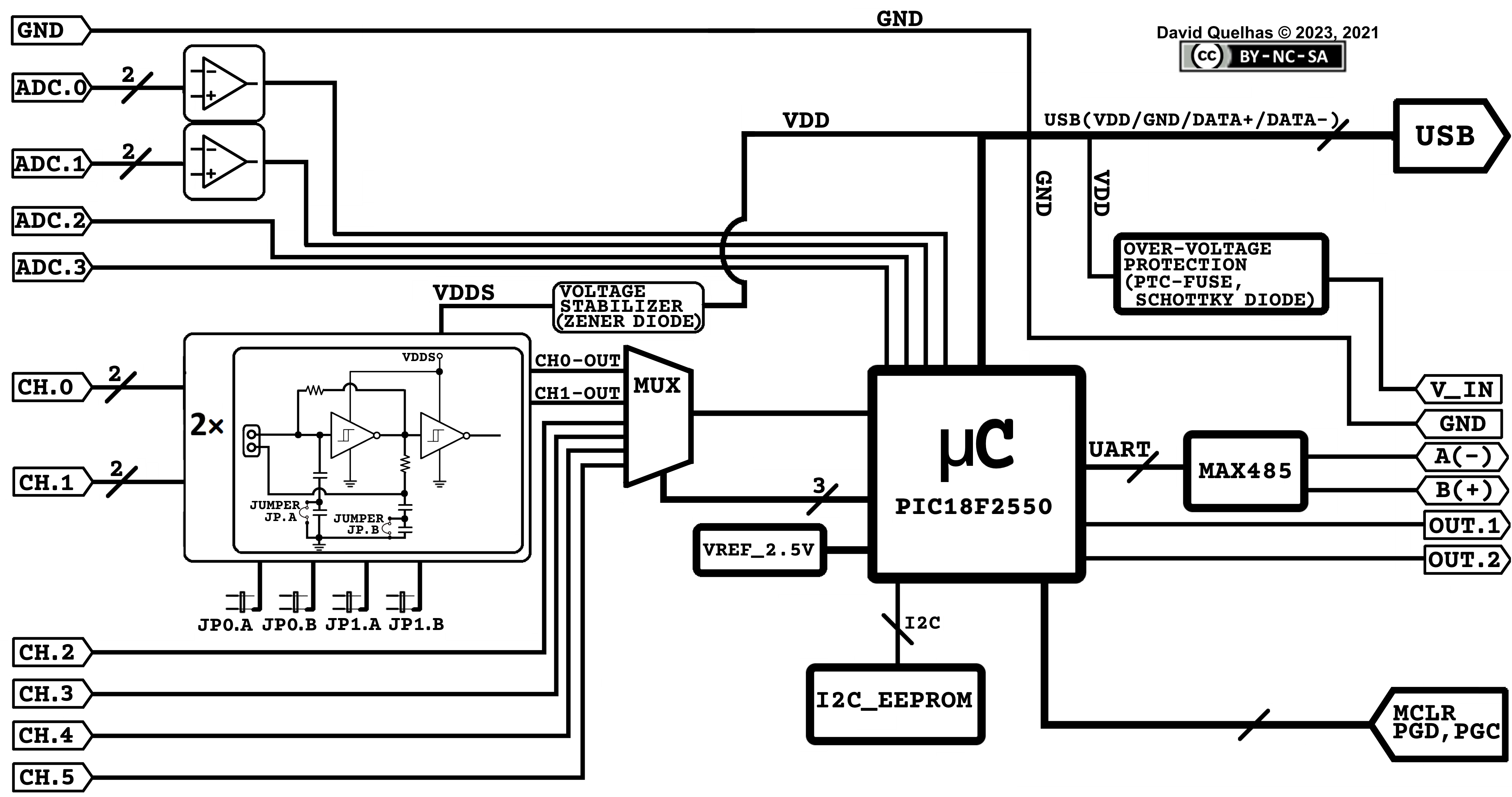
Here is presented the Multiple Sensor Interface (Fig.1), the interface main components / sub-circuits are: The connectors and sensor interface circuits (oscillators) for inductance, resistance, capacitance, and frequency (CH.0, CH.1); the connectors and over-voltage protection(zener diode) for frequency measurement (CH.2, CH.3, CH.4, CH.5); the connectors and interface circuit for voltage measurement (ADC.0, ADC.1, ADC.2, ADC.3); analog multiplexer for the sensor channels, the microcontroller (PIC18F2550); I2C EEPROM for storing calibration tables; USB connector; connector and circuit for RS-485 and UART; digital outputs connector (OUT.1, OUT.2).
The digital outputs have the value of a boolean function defined by the user, boolean functions with logic variables that are the result of a comparison (’bigger’ or ’smaller’ than), between the value/measurement of a sensor channel and a configurable threshold value. The connectors used for frequency measurement may be connected to external single sensor interface circuits (oscillators).
2.2 The sensor interface circuit (oscillator)
The sensor interface (Fig.2) is an oscillator with a circuit design based on the Pierce oscillator with some modifications. The 1st difference is that there is no quartz crystal, and on the location of the crystal will be connected the sensor to be measured (variable inductance or resistance or capacitance), the 2nd difference is that instead of simple inverters (’NOT’ gates) will be used Schmitt-trigger inverters(high-speed Si-gate CMOS, 74HC14), this is a very relevant difference that will allow the oscillator to work even with a resistive or capacitive sensor, in fact the interface circuit works with sensors mostly as Schmitt-trigger oscillator. Also the Schmitt-trigger inverters output a noise-free square-wave signal, as oscillator or as external signal converter.
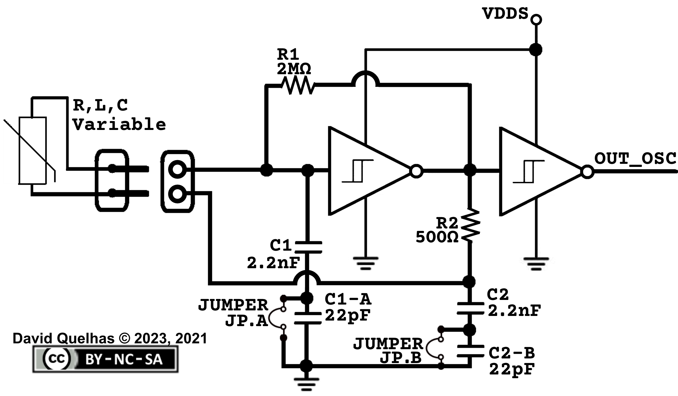
The sensor interface circuit has 2 pairs of series capacitors (C1 2.2nF, C1-A 22pF and C2 2.2nF, C2-B 22pF) instead of just 2 capacitors(C1,C2) so the value of C1 and C2 can be adjusted just by placing/removing a jumper; placing a jumper removes C1-A or C2-B from the circuit making 2.2nF the value of C1 or C2; removing the jumper lets the capacitors in series making 21.78pF the total value of (C1, C1-A) or (C2, C2-B). So on the rest of the article, whenever is mentioned C1 or C2 is meant the resulting capacitor value that can be 2.2nF(jumper on) or 21.78pF(jumper off), accordingly with mentioned jumper configuration.
The sensors can be connected directly on the Multiple-Sensor Interface(on the screw terminals/connectors), or by using a cable; for a cable longer than 20cm is recommended the use of shielded twisted-pair(STP) cable to prevent cross-talk between sensor channels or external EMI.
2.3 Measurement process
The Multiple-Sensor device has a microcontroller (PIC18F2550) that is able to make frequency and voltage measurements, so the device makes frequency measurements for sensor channels CH.0 to CH.5 ; and makes voltage measurements for sensor channels ADC.0 to ADC.3; these frequency and voltage measurements made by the device are designated as the raw_value of a sensor channel. To obtain the measurement of a sensor channel, the device uses a 2 column calibration table, that is a long list of points (raw_value; measurement) relating the measurement value (obtained during calibration by an external reference device) to the corresponding raw_value obtained on the Multiple-Sensor device, these calibration tables are stored on an I2C EEPROM memory on the Multiple-Sensor device.
The Multiple-Sensor device can work in two modes: single-channel or multiple-channel, the CH.0 to CH.5 raw_value(frequency) are calculated through a counter/timer of the PIC18F2550 by periodically reading its value and calculating the frequency f=count/period ([Hz]=[cycles]/[s]). So in single-channel mode the frequency is always calculated on the selected/enabled sensor channel, in multiple-channel mode the frequency is calculated for each sensor channel sequentially (time-division multiplexing), since there are 6 channels to measure but only on counter/timer of the microcontroller for that job. Thus in multiple-channel mode a measurement takes 6x more time to be updated/refreshed than in single-channel mode.
For the sensor channels ADC.0 to ADC.3 the raw_value is the voltage of those channels measured by using the ADC (Analog to Digital Converter) of the microcontroller and also reading a 2.5V voltage reference.
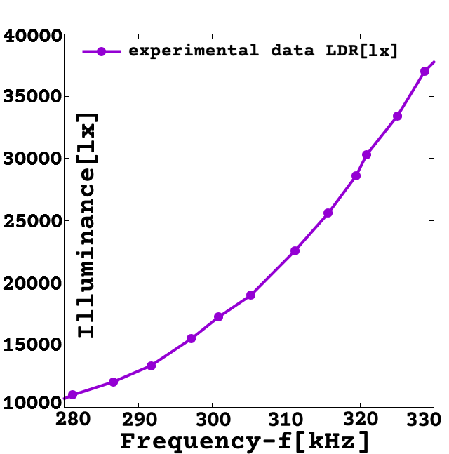
The sensor measurements are calculated by searching the raw_value on the corresponding calibration table, and by using from the table 2 points (raw_value,measurement) referenced here as points P and Q such that the measured raw_value is bigger than raw_value of P and is lower than raw_value of Q; then is calculated a linear equation: , defined by the points P and Q. So every-time the device calculates a sensor measurement, it will calculate the corresponding linear equation for the current raw_value and use it to obtain the current measurement (Fig.3) .

2.4 Device calibration for a sensor
Device calibration is about obtaining calibration tables for each sensor channel, here are 2 ways to obtain it:
1- Do a full manual calibration using an external meter as reference where both the reference meter and the Multiple-Sensor device(with a sensor connected) are exposed to same stimulus/environment that is controllable by the user to produce all adequate variations/intensities necessary to record an extensive calibration table, with all experimental pairs of (raw_value,measurement).
2- Using a known function that relates the measured phenomena to the obtained raw_value on the Multiple-Sensor device (obtained by theoretical or experimental study), although a purely theoretical calibration could be used, probably is better or easier to obtain a calibration table by using a known function and have its constants/parameters calculated by a data fitting to some few experimental data points (raw_value, measurement) obtained for the device calibration. So for example if the known function had 3 constants/parameters, you would require at least 3 different experimental measurements to obtain the function for that sensor channel, then having the function is just a question of calculating a longer list of pairs (raw_value,measurement) on the desired measurement range. Fig.4 is the result of fitting the model function , to the points: (244Hz, 0.01 [lx]), (25320Hz, 30 [lx]), (232041Hz, 3950 [lx]); obtaining the values: 80.2359; 79.8743; 1.79972. The symbol e is the Euler-Napier constant. The point at 244Hz was changed from 0[lx] to 0.01[lx] as it may facilitate/improve the model function fit.
3 Results and Analysis
3.1 Device testing
The author developed and built prototypes of the described device, made of the components described in the previous section and in Fig.1 diagram. Then the device was experimented with various different sensors; including various common sensor components, namely: LDR (Light Dependent Resistor or also designated as photo-resistor), RTD(Resistance Temperature Detector), FSR(Force Sensitive Resistor), Relative-Humidity sensor (RH to impedance); as well some handmade sensors done by the author for the purpose of exploring the device usability, namely: a water level sensor (by variation of capacitance based on water height), a proximity sensor (based on the variation of inductance of a flat coil, caused by the vicinity of a metallic object, or the vicinity of a non-metallic object covered with aluminum or copper adhesive tape), a force sensor (based on resistance variation when pressed) made using ’carbon impregnated foam’ (also known as ESD/antistatic foam), aluminum foil and adhesive tape.
The tests done with the device connected on the various mentioned sensors, were made with the purpose of verifying that the device is indeed usable with various types of sensors, but those tests are not the most appropriate for studying how the device works, or for characterizing the device itself by determining its usability range, or for gathering quantitative data about the device to be used along with the data from a sensor datasheet for determining its compatibility.
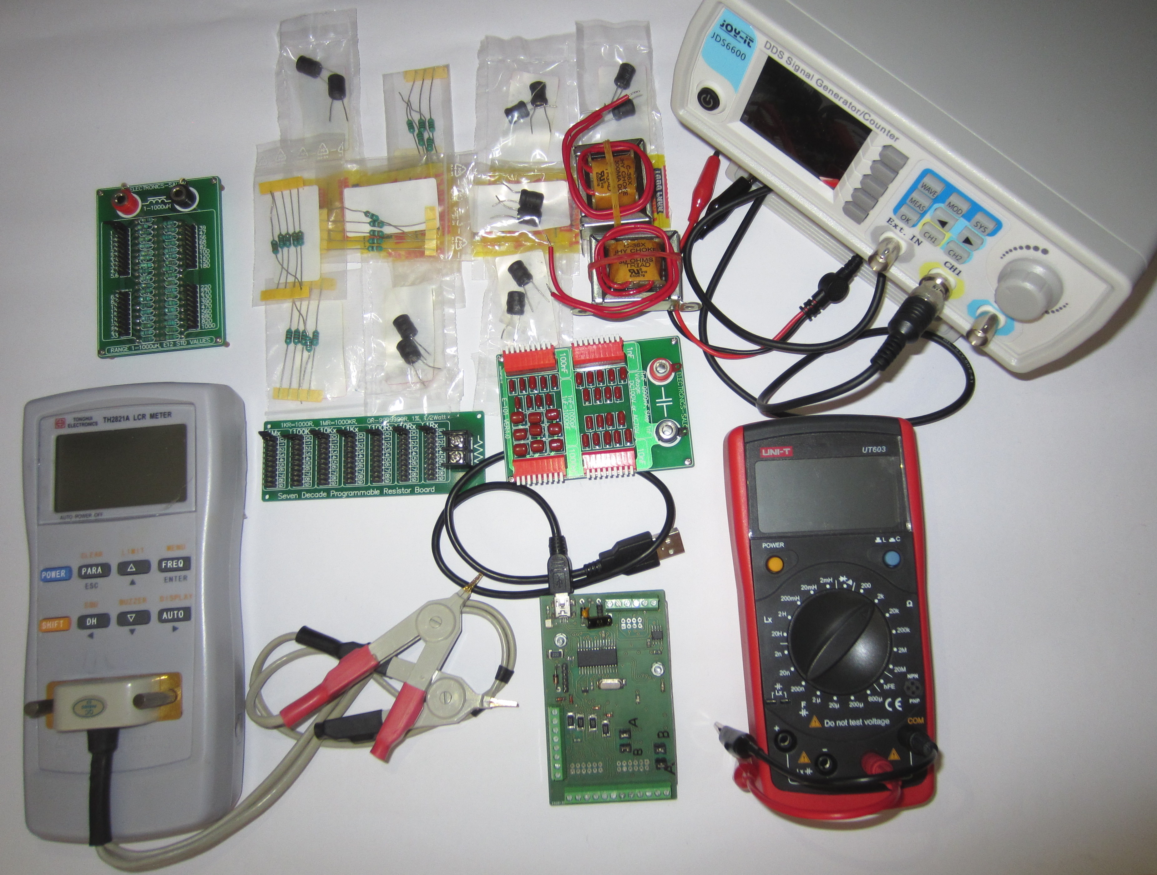
So the tests chosen for characterizing the device were records (in 2 column tables) of the measured values of inductance, resistance, capacitance paired with measured frequency on the Multiple Sensor Interface device. For these tests (Fig.5) were used arrays(PCBs) of inductors, resistors, capacitors that allow to obtain various different values just by changing a jumper/switch, also were used single components (including in series or parallel association); these fixed value components were connected as the sensor on the device. The various figures with plots/graphs in this article will show both the experimental data obtained from the mentioned tests, as well the theoretical graphs obtained from circuit analysis of the device, for comparison purposes.
The experimental data of the mentioned tests is on:
Appendix A ( Tab. 1, Tab. 2, Tab. 3 ) is the , , tables with , as 2.2nF(JP on) or 21.8pF(JP off); Appendix B ( Tab. 4 , Tab. 5 , Tab. 6 ) is the , , tables with , as 93nF(JP on) or 21.8pF(JP off); Appendix D ( Tab. 7 ) is the table with ==2.2nF(JP on) of a LDR sensor.
3.2 Sensor Interface Circuit Analysis
3.2.1 Multiple-Sensor Interface for inductive sensors
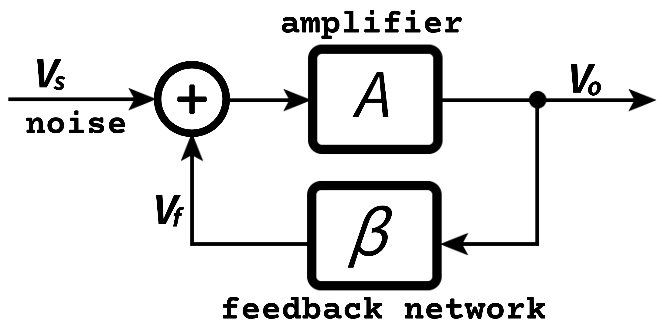
When is connected an inductor or inductive sensor the Multiple-Sensor Interface (Fig.2 ) may work as a Pierce oscillator(where the sensor is connected instead of a quartz crystal). The theoretical analysis for this type of oscillator, can be based on a model of 2 circuit blocks named ’A’ and ’’ connected for feedback by connecting the output of one to the input other. The ’A’ is an electronic amplifier providing voltage gain, the ’’ is an electronic filter providing frequency selection (resonance), so whatever voltage signal amplified by ’A’ is frequency selected by ’’ and feed back to the input of A for further amplification. As known, this oscillator is start-up by whatever noise () available at the input of ’A’, Fig.6 is a diagram depicting this concept.
With this type of oscillator, for determining the frequency of oscillation, may be used the Barkhausen stability criterion that says to be possible to occur sustained oscillations (oscillations on steady state analysis); where and represent the transfer function of the correspondingly named block.
The circuit analysis of the Pierce oscillator is available on various text book (and also class notes); references about Pierce oscillator circuit analysis that are the author preference for understating how the Multiple-Sensor Int. may work as Pierce oscillator, are: "Crystal Oscillators" of "Digital Electronics" class notes by Peter McLean [2] ; "Microelectronic Circuit Design (4th ed.)" by R.C. Jaeger, T.N. Blalock [3] ; "Microelectronic Circuits (8th i. ed.)" by A. S. Sedra, K. C. Smith, T. C. Carusone, V. Gaudet [4] .
About the circuit analysis of the Pierce oscillator (and in generally with Colpitts type oscillators), a relevant conclusion is that the feedback network (block ) composed of 3 electrical components, that include the capacitors and , must have an inductive part on the remaining (3rd) electrical component (for example: the piezoelectric crystal of a typical Pierce oscillator, or simply an inductor, or an inductive sensor, etc…), to be able to satisfy and so have oscillations on steady state analysis.
For the Pierce oscillator the equation that relates the oscillation frequency with the inductance and capacitance is a typical equation of LC oscillator circuits, using the definition of a "load capacitance" as .
The frequency of oscillation on the Pierce oscillator (using , , ) is:
| (1) |
So the expression (theoretical) of a value for inductance () as a function of frequency(f) is:
| (2) |
On experimental tests done was observed that when using ==2.2nF (JP.A and JP.B closed) or when using =21.78pF (JP.A open), =2.2nF (JP.B closed), with decreasing values of connected, the oscillation frequency exhibited a sudden change, at some small value of L(around for ==2.2nF), not coherent with theoretical model of Pierce oscillator. This may be related to the fact that the same circuit also implements a Schmitt-trigger oscillator(next section), that oscillates under different criteria, so the author opinion is when approaches some small value it may change from Pierce oscillator to Schmitt-trigger oscillator. Fig.8 and Fig.8 shows the experimental data for various inductance values connected as the sensor and the plot using (2) with ==2.2nF and =21.78pF, =2.2nF.
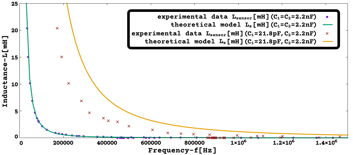

Since the mentioned sudden change of oscillator mode and frequency is not adequate on a function usable for sensor interfacing; then on experimental tests with jumper configuration: JP.A on and JP.B off (=, =21.78pF), it was observed a continuous and progressive function. With =2.2nF, =21.78pF, the experimental values followed a straight line for in (Fig.10), then for 100 the experimental has a shape with some visual similarity to theoretical (as Pierce oscillator), but with very different values. Also apparently for larger values of the theoretical (Pierce oscillator, JP.A on, JP.B off) could be approximated to the experimental data by a constant multiplicative factor (, for 1mH), as visible in Fig.10.
For modeling(data fitting) purposes, the author knows that a function , where ’a,b,c,d,m,n’ are constants to fit, can be fitted to experimental data on both low and high values of .


On following section 3.3 was used an approximated model (for Schmitt-trigger oscillator) applied to Multiple-Sensor Interface with inductive sensor (JP.A on, JP.B off), that exhibited a theoretical plot much closer to the experimental data, corroborating the hypothesis that with jumper configuration JP.A on, JP.B off (=2.2nF, =21.78pF), it operates as a Schmitt-trigger oscillator, where acts as an impedance influencing charge and discharge speed.
On following section 3.4, also about inductive sensor (JP.A on, JP.B off), was used a theoretical model(for Schmitt-trigger oscillator) with some rude/obscene approximations; that model was successful in predicting the correct shape of although with a somewhat considerable displacement to the experimental data.
3.2.2 Multiple-Sensor Interface for resistive sensors
In case you connect a resistive sensor (or capacitive) to the Multiple-Sensor Interface it will not be able to satisfy the conditions for oscillation consequent of the Barkhausen criterion applied to the circuit as Pierce oscillator. So the conclusion is when you connect a resistive sensor (or capacitive) you no longer have a Pierce oscillator. The Multiple-Sensor Interface is made using Schmitt-trigger inverters(high-speed Si-gate CMOS, 74HC14), and the hysteresis of the Schmitt-trigger can be used to implement another type of oscillator, the relaxation oscillator. So in the case of a resistive sensor the circuit to analyze is a Schmitt-trigger inverter connected to a network of resistors and capacitors.
To analyze this circuit the Schmitt-trigger inverter was replaced by a theoretical switch that changes the voltage of node to (power supply stabilized voltage for the sensor interface) when voltage is lower than , and changes to GND when voltage is higher than .

So the circuit of Fig.11 is here analyzed to obtain , and then its inverse function that may be useful for using/configuring the Multiple-Sensor Interface. Notice that 0 since is the input of a Schmitt-trigger inverter (high-speed Si-gate CMOS) that has a very high input impedance and so 0 is an appropriate approximation simplifying the circuit. So from the circuit are obtained the equations: Nodes and loops: ,
, , , ,
, , , , , .
Components: , , , , .
Solving:
| (3) |
| (4) |
Solving:
So using the previous result the (4) can be changed to:
| (5) |
Solving (3) for is obtained:
| (6) |
Calculating the derivative on both sides of (6) is obtained (remember is a constant equal to or GND depending on the position of the switch ’SW’):
| (7) |
Now using (6) and (7) to remove the variables and from equation (5) is obtained an equation solvable for determining :
| (8) |
The equation (8) is of the type: that has the general solution: , where , are integration constants to be defined by ’initial conditions’ and , are defined by: and e is the Euler-Napier constant .
So defining here , , as the values of a, b, c for obtaining when using a resistive sensor, as:
,
,
.
In order to obtain for this circuit is required to calculate and , that are constants to be defined by ’initial conditions’, the value of these constants is related to the voltage (or electrical charge) on capacitors and at the moment the inverter gate changes its output voltage (high to low, or low to high), on the model used for analyzing the circuit that is when the ’theoretical switch’ changes state. Also, is only known the value of (to be or ) when the inverter gate changes value, so is very difficult to calculate both and by algebraic manipulation. Admitting that and that (that is the case of the circuit that was studied and tested where and ), then is known that the capacitor will charge faster than for all values of , and in case has an impedance comparable to then will charge much faster than . So the voltage (and electrical charge) of follows closely the values of and so will be of small relevance to the initial conditions of the circuit, thus can be approximated as single exponential function , this approximation is implied on the following calculations.
Is selected the solution by setting , because is the one that provides an adequate value for , , consistent with experimental data, however for obtaining the (approximate) function you may use any.
For convenience of a more similar to typical RC circuits is defined , and so (or more appropriately: ).
Charging time of :
Discharging time of :
The time for a complete cycle of charge and discharge of is: ; the frequency of is .
Solving:
For convenience defining the constant ’H’ by:
,
then .
So the expression (theoretical) of an approximate value for resistance () as a function of frequency(f) is:
| (9) |
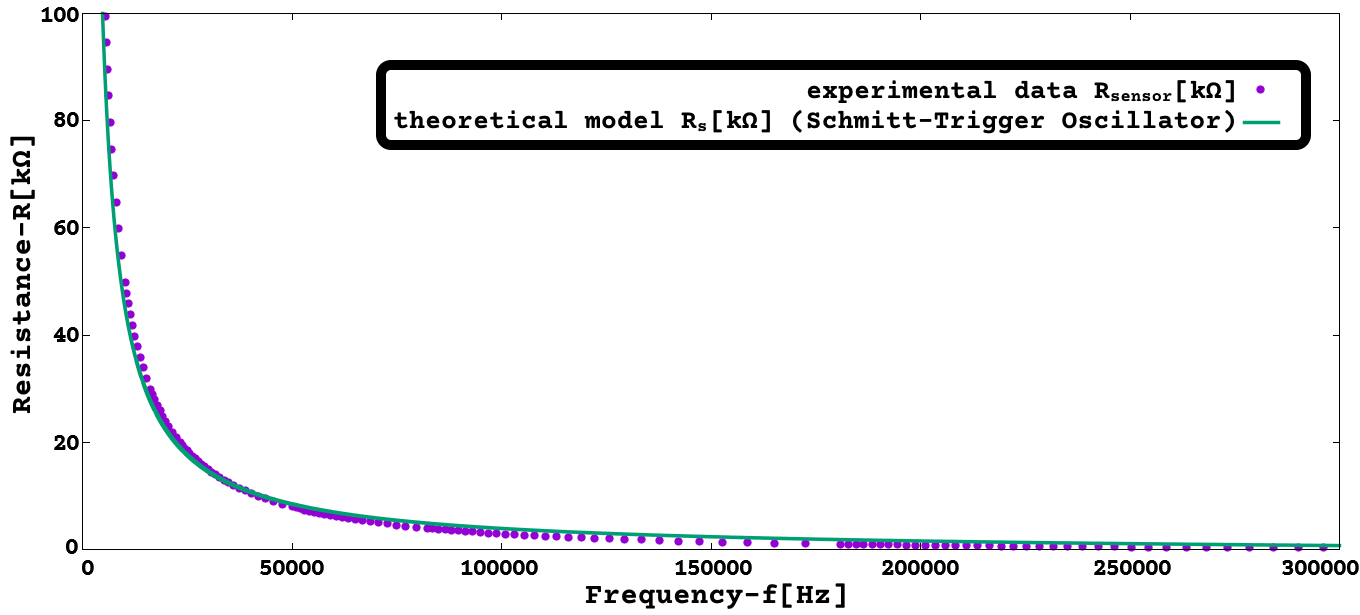
Using the values , , , , , , is obtained , Fig.12 shows experimental data for Multiple-Sensor Interface with various resistance values connected as the sensor and also shows using (9) with the mentioned values of , , , , .
3.2.3 Multiple-Sensor Interface for capacitive sensors
In case you connect a capacitive sensor (or resistive) to the Multiple-Sensor Interface it will not be able to satisfy the conditions for oscillation consequent of the Barkhausen criterion applied to the circuit as Pierce oscillator; and so it is again a Schmitt-trigger relaxation oscillator. To analyze this circuit the Schmitt-trigger inverter was replaced by a theoretical switch (Schmitt-trigger), just like previously with resistive sensors.

So the circuit of Fig.13 is here analyzed to obtain , and then its inverse function that is useful for using/configuring the Multiple-Sensor Interface. Notice that 0 since is the input of the Schmitt-trigger inverter(high-speed Si-gate CMOS) that has a very high input impedance and so 0 is an appropriate approximation simplifying the circuit. So from the circuit are obtained the equations:
Nodes and loops: , ,
, , ,
, , , , , .
Components: , , , , .
Solving:
| (10) |
| (11) |
| (12) |
Since then , and so using it on equation (10), is obtained:
| (13) |
Calculating the derivative of (14) is obtained:
|
|
(15) |
Now using (14) and (15) to remove the variables and from the equation (12), is obtained an equation solvable for determining :
|
|
(16) |
The equation (16) is of the type: , that has the general solution:
, where , are integration constants to be defined by ’initial conditions’ and , are defined by: and e is the Euler-Napier constant .
So defining here , , as the values of a, b, c for obtaining when using a capacitive sensor, as: ,
,
.
In order to obtain for this circuit is required to calculate and , to be defined by ’initial conditions’; notice that this circuit has 3 capacitors that store electrical charge defining ’initial conditions’, but the location of connected between and implies that the voltage of (or its electrical charge) is completely defined/known by the voltages (or electrical charges) on and .
Here are made the same approximation/simplification of , as explained and done on the case of resistive sensor.
Is selected the solution by setting , because is the one that provides an adequate value for , , consistent with experimental data, however for obtaining the function you may use any.
For convenience of a more similar to typical RC circuits is defined , and so (or more appropriately: ).
So when is connected a capacitive sensor () the differential equation and solution are the same as when is connected a resistive sensor (), the only differences are in the values of , , ; and as such the equations of (frequency) and (period) are also the same and are reused from the previous section.
The constant ’H’ defined by:
,
and .
So the expression (theoretical) of an approximate value for capacitance () as a function of frequency(f) is:
| (17) |
Using the values , , , , , , is obtained , Fig.14 shows the plot of using (17) with the mentioned values of , , , , .
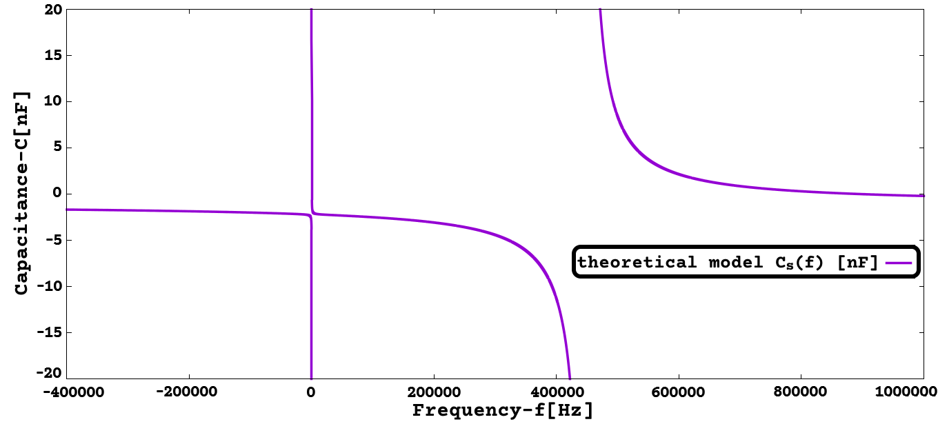
Analyzing the plot in Fig.14 by firstly looking at plot regions with 0, its visible that the plot is close to being over the vertical axis (f=0) and this would mean that for all values of the frequency would be close to zero (), but visible to the right is another curve that is also placed on the area of 0 ( for frequency [447957Hz, 895689Hz] ) and at a first view this curve would seem appropriate. But strangely on 0, f0 for each value of are 2 values of frequency, while for 0, f0 each value of has only one possible value of frequency (f0 is considered meaningless/ignored).
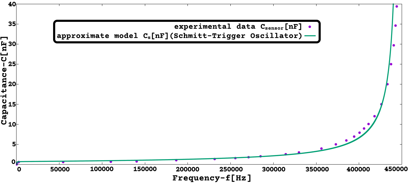
The experimental data shows that the way the oscillator works using a capacitive sensor is different from what some would expect on a first view of the plot , in order to compare the experimental data with the theoretical model is shown in Fig.16 and Fig.16 the experimental data for Multiple-Sensor Interface with various capacitance values connected as the sensor and also the plot of () using (17) with the mentioned values of , , , , .
So it seems that the obtained function of although strangely indicates negative values for the sensor capacitance it can provide a theoretical curve/plot similar to what was obtained on the experimental data for . On the following sections is given a better insight on why has a negative value.


3.2.4 Multiple-Sensor Int. for measuring frequency
For measuring frequency of an external voltage signal (between 0V and , so preferentially a digital signal or in case of analog signal it should be limited/trimmed before) is possible to use the mentioned Multiple-Sensor Interface and so using the same port/connector of the device. For this the user should remove/open the jumpers "JP.A", "JP.B" making the capacitors C1-A, C2-B active on the circuit, this will make that is a quite low capacitance that will have an insignificant effect on the external voltage signal. The external voltage signal should be connected to the 1st pin of the sensor channel that is the one connected directly to the input of the Schmitt-trigger inverter, so that the inverter is directly driven by the external voltage signal, then the Multiple-Sensor Interface is just a converter of the voltage signal to a square wave signal where its frequency will be measured through the counter/timer of the PIC18F2550.
The external voltage signal would preferentially be from a sensor with a square wave output, and the sensor have its power supplied by one of the ,GND ports/connectors of the sensor interface device or by an external connection to the same power supply used to power the device.
3.3 Alternative Approximate Circuit Analysis
3.3.1 Sensor interface circuit simplified
The Multiple-Sensor Interface circuit when working as Schmitt-trigger oscillator (using , , or with specific , values) can be studied and understood in a more intuitive way by making some simplification/approximation that may be inaccurate for quantitative purposes but still captures its essence, with the benefit of exposing how it works and resulting in much simpler differential equations. So the interface circuit is a more complex Schmitt-trigger oscillator, but its essence is the same, it is just some capacitors being charged by currents that pass through some resistors, and the voltage on a capacitor() will trigger(at or ) a switch(electronic inverter) to change the voltage() [5] .
So the sensor and interface circuit can be described approximately as a basic Schmitt-trigger oscillator that only has one capacitor and one resistor (that determine the frequency of oscillation), and so was used the simplified circuit in Fig.17 where is a capacitor and is a resistor that approximate in overall the capacitance and resistance of the sensor interface oscillator.
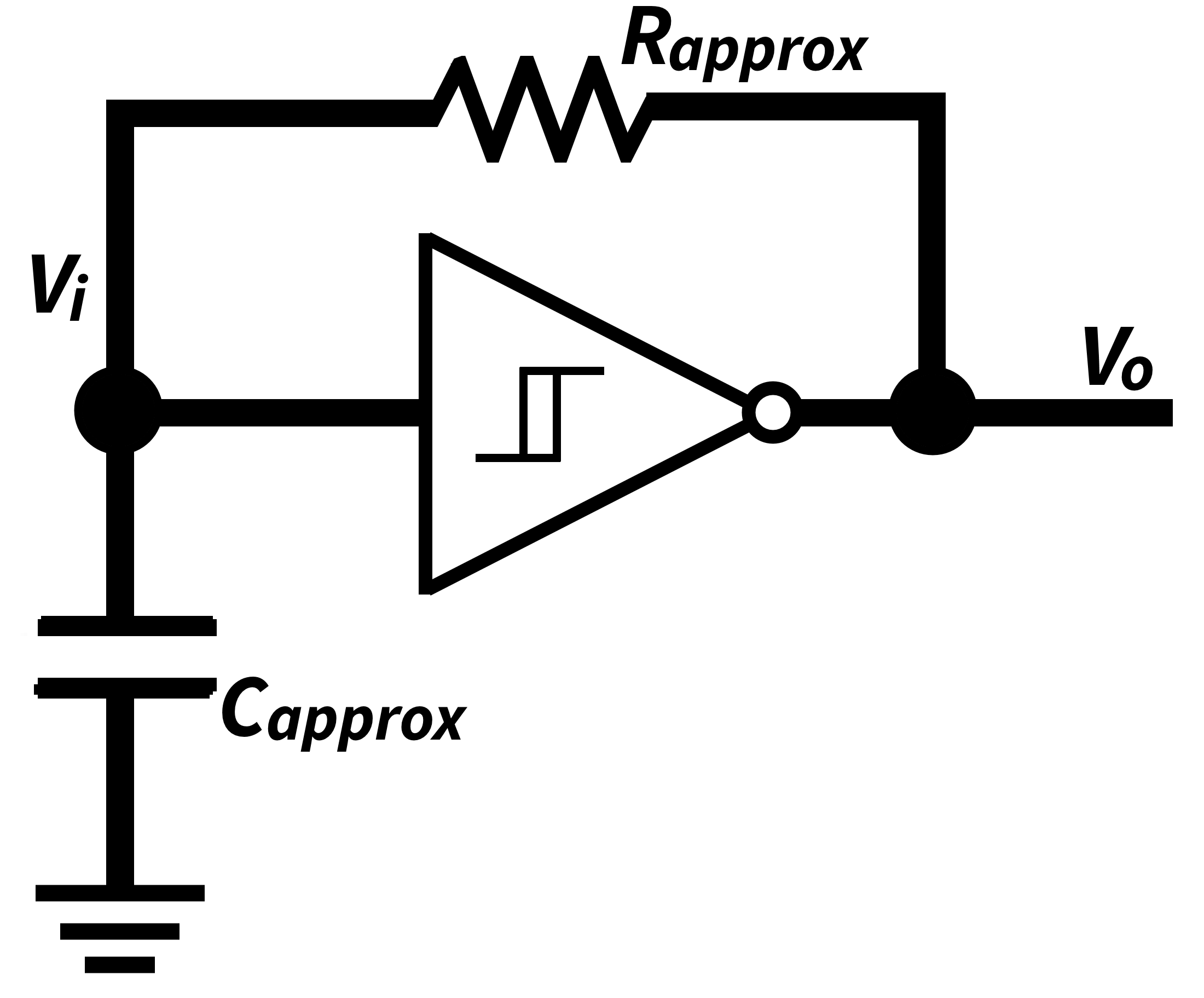
To build expressions of and that include , , , are considered initially 2 extreme cases of the sensor impedance(): 1st the sensor can be replaced by a wire, and 2nd the sensor can be removed(open circuit), these 2 extreme cases possible for the sensor impedance are represented in Fig.18 .
Now the sensor can be described as an electric connection that can be weakened or intensified depending on the sensor impedance, so when changes progressively from 0 to the circuit behavior changes progressively and smoothly from the behavior of the left circuit to the behavior of right circuit of Fig.18. So to obtain equations for and was selected an expression that allows to change smoothly the resistance and capacitance of the left side circuit to the resistance and capacitance of the right side circuit of Fig.18.

So as in Fig.18, here are the values of and for the 2 extreme values of and :
; ;
; ;
3.3.2 and for a resisitve sensor ()
Here are functions modeled to describe and (with resistive sensor) with a smooth transition from its values at and , where :
| (18) |
| (19) |
Using the equations: , and using , where was removed using , it can be obtained .
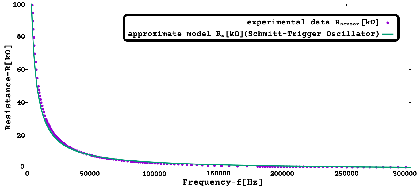
Using values , , , is obtained (valid for any type of sensor).
Using the values , , , with the approximate model (, ), is obtained the plot of in Fig.19.
3.3.3 and for an inductive sensor ()
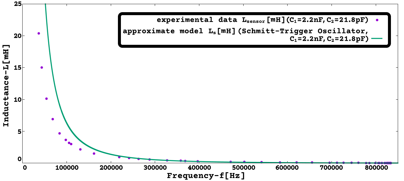
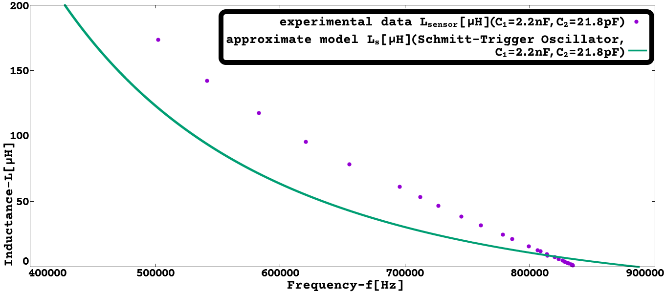
This approximate model for the interface circuit with inductive sensor is only valid for jumper configuration(capacitor values) that make it work as Schmitt-trigger oscillator, as is expected for JP.A closed, JP.B open (=2.2nF, =21.78pF). Here are functions modeled to describe and (with inductive sensor) with a smooth transition from its values at and , where :
| (20) |
| (21) |
Using the values =2.2nF, =21.78pF, , , with the approximate model (, ), is obtained the plot of in Fig.21 and Fig.21.
3.3.4 and for a capacitive sensor ()
Here are functions modeled to describe and (with capacitive sensor) with a smooth transition from its values at and , where :
| (22) |
| (23) |
Using the values , , , , with the approximate model (, ), is obtained the plot in Fig.23 and Fig.23.

3.4 Multiple-Sensor Interface for inductive sensors as Schmitt-trigger oscillator
Also is possible a theoretical analysis of the Multiple-Sensor Interface with an inductive sensor working continuously as a Schmitt-trigger oscillator observed when jumper configuration is JP.A on, JP.B off (=2.2nF, =21.78pF), although some approximations were required to be able to obtain a function.

So the circuit of Fig.24 is here analyzed to obtain an approximation of , and of its inverse function that is useful for using/configuring the Multiple-Sensor Interface. Notice that 0 since is the input of the Schmitt-trigger inverter(high-speed Si-gate CMOS) that has a very high input impedance and so 0 is an appropriate approximation simplifying the circuit. So from the circuit are obtained the equations:
Nodes and loops: , ,
, , ,
, , , , , .
Components: , , , , .
Solving:
| (24) |
| (25) |
| (26) |
From (25) is obtained , and so using it on equation (24), is obtained:
| (27) |
From equation (26) is obtained:
| (28) |
Using (28), can be eliminated from eq. (27), obtaining:
| (29) |
The equation (29) is of the type: that has the general solution: , where ,, are integration constants to be defined by ’initial conditions’ and , , are defined by: and e is the Euler-Napier constant .
So defining here , , , as the values of a, b, c, d for obtaining when using an inductive sensor, as:
, ,
, .
In order to obtain for this circuit is required to calculate , and , that are constants to be defined by ’initial conditions’, the value of these constants is related to the voltage (or electrical charge) on capacitors and , and also to the electric current on the inductive sensor, at the moment the inverter gate changes its output voltage (high to low, or low to high), on the model used for analyzing the circuit that is when the ’theoretical switch’ changes state. Also, is only known the value of (to be or ) when the inverter gate changes value, so is very difficult to calculate , , by algebraic manipulation. Admitting that and that (that is the case of the circuit that was studied and tested where and ), then is known that the capacitor will charge faster than for all values of (determined by the value ), and in case has an impedance comparable to then will charge much faster than . So the voltage (and electrical charge) of follows closely the values of and so will be of small relevance to the initial conditions of the circuit.
The inclusion of an inductor (the inductive sensor) makes the behavior of this circuit more complex and so the appearance of a 3rd degree differential equation; so in order to obtain an expression for in a similar way as previously for resistive and capacitive sensors, are made the following approximations: 1 - The determination of will be made in two domains, one expression of valid for high frequency and other expression of for low and middle frequency of the operation of the Schmitt-trigger oscillator. The author observed that high frequency operation is dominated by the 1st-root of that is a real number; and observed that low and middle frequency operation is dominated by the 2nd-root and 3rd-root of that are imaginary numbers.
2 - Regarding the low and middle frequency operation that is dominated by the 2nd-root and 3rd-root of the 3rd degree equation, will be made a ’rude’ approximation of , where and . Also is relevant to note that by adding with will nullify the imaginary part resulting in a real number, and also that .
3 - Regarding the high frequency operation that is dominated by the 1st-root of the 3rd degree equation, will be made the approximation of .
The mentioned approximations resulting in , allows the theoretical analysis already used for resistive and capacitive sensor to be reused again here, for obtaining an approximation of .
So for an inductive sensor, just like with resistive or capacitive sensor, is used the function , where , and the constant ’H’ defined by:
,
and .
So applying the previously mentioned approximations is obtained: ; .
So the expression (theoretical) of an approximate value for inductance () as a function of frequency(f) for high frequency is:
| (30) |
So the expression (theoretical) of an approximate value for inductance () as a function of frequency(f) for low and middle frequency is:
| (31) |
Using the values , , , , , , , is obtained , Fig.25 shows the plot of using (30) with the mentioned values of , , , , .
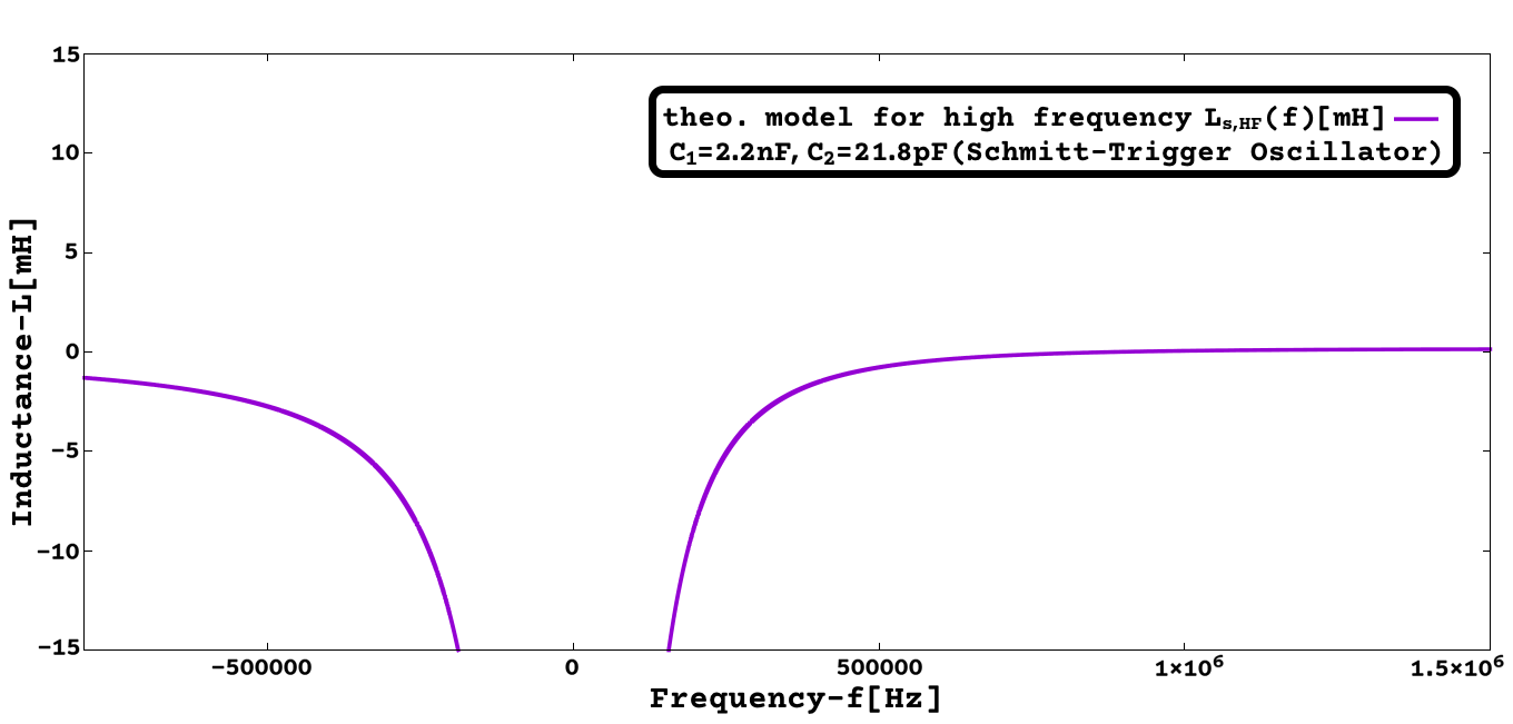
Observing Fig.25 is noticeable that is almost always negative, except for frequency above around 900kHz. However drawing the plot of () along with experimental data for Multiple-Sensor Interface with various inductance values connected as the sensor (in Fig.27 and Fig.27 ), like was done before for the plots of a capacitive sensor, is then visible that the shape of resembles the experimental data, however significantly displaced above the experimental data for low and middle values of frequency, but for high frequency the plot of is much closer to the experimental data and correctly predicts that a value of will result on an oscillation frequency somewhat above 800kHz but lower than 900kHz.


The Fig.29 and Fig.29, shows experimental data for Multiple-Sensor Interface with various inductance values connected as the sensor, and the plot of using (31) with the mentioned values of , , , , . Observing Fig.29 and Fig.29 is noticeable that follows the experimental data on low and middle frequency (however with some displacement), but for high frequency has a large displacement to the experimental data and fails to predict the frequency at =0.
A way for obtaining a theoretical function (by previously mentioned approximations/simplifications) valid for all values of frequency, that captures the behavior of the Multiple-Sensor Interface with an inductive sensor, is to combine both the expressions and into a single function. That function can be obtained for example by multiplying with a moderating function that silences it on low and middle frequency and by multiplying with a moderating function that silences it on high frequency, then sum these 2 parts to obtain .
A set of 2 good moderating functions, considering the used values of , , , , , would be for example:
These moderating functions are good because: +1, , and also:
(0)0; (900kHz)1;
(+)1; (+)0;
(0)1; (900kHz)0;
(500kHz)(500kHz)0.5 .
However the moderating functions , are exponential functions that are undesirably complex and heavy to evaluate; so here is suggested another set of 2 moderating functions that are simpler and faster to evaluate, although the property +1 will only be true on a small frequency range and that will cause some distortion (undesirable change) on the theoretical model. Since the theoretical model is not accurate because of the approximations that were used for obtaining a solution to the initial value problem (that had 3 unknowns , , , but was solved as if had a single unknown), and also knowing that is always above the experimental data and that is above the experimental data on a portion of the plot (on this situation for f>250kHz), then can be selected moderating functions that have a ’distortion’ that actually approximates(lowers the value of) and to the experimental data.
A set of 2 moderating functions that are more simple and fast/easy to evaluate, but ’distort’ (lower) the value of :
| (32) |
| (33) |
Also let’s have in consideration a frequency value defined as == (the frequency where the plot of reaches the horizontal axis of ).
Then, =.
So by first determining the frequency for some selected values of the parameters , , , , , then is possible to create/define as a ’theoretical’ function (by the previously mentioned approximations/simplifications) through , , to be valid for all values of frequency:
|
|
(34) |
The calculation of and to create some moderating functions , may be done for example by defining target values of =, =, by this method is obtained:
| (35) |
| (36) |
So the constant may be selected/adjusted so that ==0.5, this is the same as to say that will be selected/adjusted so that when frequency is at 2/3 of then will be 50% of .
So the constant may be selected/adjusted so that ==0.01, this is the same as to say that will be selected/adjusted so that when frequency is at then will be 1% of .
So for this case (, , =2.2nF, =21.78pF, ), with ==0.5, ==0.01, was selected/adjusted the values: , (Fig. 30).

The Fig. 32 and Fig. 32, shows experimental data for Multiple-Sensor Interface with various inductance values connected as the sensor, and the plot of using (34) with =2.2nF, =21.78pF, , , , , .


4 Discussion
The experimental data obtained when testing the Multiple-Sensor Interface is in overall close to the values calculated using the formulas obtained from the circuit analysis, as it is visible on the various figures that show the plots of the experimental data along with graphs done using the mentioned formulas. In some graphs, there was a deviance or offset between the theoretical and experimental quantitative values, however the observable deviations are not reason for concern as they never affected the similitude between theoretical and experimental graphs (with exception of Fig.10 and Fig.10 that as explained, when using that specific configuration the device no longer behaves as Pierce oscillator, but instead as a Schmitt Trigger oscillator, as it was shown on later subsections). The information that is made available on the article, besides explaining how the device works, may also be useful for a user of the device/technology for determining if a specific sensor of his interest is compatible/usable when connected to the Multiple-Sensor device, namely by observing on the graphs (or tables), for what range of values (min. and max.) of the sensor electrical quantity ( or or ) it is verified that a change on the quantity the sensor is measuring will produce/cause also a significant or measurable change of the signal frequency on the output of the oscillator used for sensor interfacing.
4.1 Future Work
Further work related to the sensor interface circuit may be developing a better understanding/prediction of why/when the Multiple-Sensor Interface with inductive sensor changes from working as Pierce oscillator to Schmitt-trigger oscillator depending on the values of and capacitors (whose values can be adjusted by jumpers JP.A and JP.B).
Other future work, outside the scope of this article, could be characterizing, testing, and comparing this sensor interface circuit for specific sensor types and/or applications, thus allowing a performance comparison with other technologies on specific use cases.
4.2 Better accuracy on a commercial scenario
A more commercial usage of Multiple-Sensor Interface possibly with better accuracy by using pre-calibrated sensors PCBs, may be:
1- Production of small single sensor PCBs that include: one sensing element (Ex: RTD, LDR, proximity inductive sensor, capacitive humidity sensor, etc …), the oscillator circuit, and a voltage stabilizer (Ex: Zener diode). The voltage stabilizer is required to obtain a stable/fixed on the sensor PCB independent of the power supply, that is already set when the producer/seller does the sensor calibration. Also the sensor PCBs should have values of and selected/tuned for best measurement range or best accuracy/precision (and so jumpers JPA/JPB not required, or may be soldered/fixed), having as output the oscillator square wave signal.
2- Obtaining a calibration table for the single sensor PCB (pairing output oscillator frequency with measurements by reference calibration instruments), on an appropriate calibration environment done/performed by the producer/seller.
3- Distribution/sale of the sensor PCBs with their own calibration table included. Could be: a calibration table printed on paper (for example: to be typed by hand on the software/application of the device, or automatically by OCR or QR-code), or as digital file that can be downloaded from the distributor/seller by using a serial number associated with the single sensor PCB.
4- An end user would connect a single sensor PCB to the Multiple-Sensor Interface device (that contains the micro-controller, EEPROM, and USB, RS-485, GPIO interfaces) on one of the frequency measurement channels (and also connect the GND), preferably using the same power supply for both the sensor PCBs and the Multiple-Sensor device. The end-user would import the provided calibration table into the Multiple-Sensor device, using the provided software/application.
Also note that with an external single sensor PCB any oscillator circuit/design may be used as long its output is a square wave signal (that doesn’t exceeds the power supply voltage); and also that a much longer distance/cable can be used between the sensor location and the Multiple-Sensor Interface device, since that any parasitic resistance/capacitance/inductance of the cable won’t affect the oscillator frequency that will be measured by the device.
The production/sale and usage scenario here described is the author perspective of a modest compromise that could be made on the hardware configurability/versatility (of the single sensor PCB with square wave signal output), that allows a producer/seller to supply ready to use sensors without any changes on the proposed hardware design of the Multiple-Sensor Interface (since it already includes 4 channels dedicated to measuring frequency of an external signal) and so without restricting the end-user ability to use any sensors it wishes or even a custom made sensor for a very specific use/application.
4.3 About (f)0 on Multi-Sensor with capacitive sensor
About (f)0 have in mind the Multiple-Sensor with capacitive sensor is studied on transient behavior (relaxation oscillator), where ’frequency’ is a measure of the speed of charge and discharge on ; and also of how fast the transient circuit analysis alternates between and .
To understand why a normal capacitor may behave as a negative capacitance when connected as the sensor of the Multiple-Sensor Interface (this is, a way to check that is possible/expected), is important to highlight some things already explored on the previous sections:
1) , .
2) The primary path (always available) to charge is through , the primary path (always available) to charge is through , since and this implies that capacitor will charge/discharge much faster(takes less time) than capacitor .
3) The purpose of sensor on this circuit is to act as a variable impedance that can establish an alternative path on the circuit () to charge/discharge capacitor ; so .
4) No matter how small may be the capacitor will always charge/discharge faster than capacitor , and on the limit where the capacitors and will be charged/discharged simultaneously.
5) The capacitors , , have same working principles, but consequence of their position within the circuit they serve different functions; so and are working as storage of electrical charge (Ex: they start discharged and end charged), while is working as a connection with ’impedance’ against charge flow (Ex: starts discharged and will end discharged, that is: and ).
For the following discussion was used as definition of capacitance the formula , where the (: [F] farad; : [C] coulomb; : [V] volt), and since the only purpose is to show how can be a negative number it was used the approximate expression that provides exactly the same sign as the exact formula; the is the average(mean) value of between and . To show is possible 0 were considered qualitative relations of the circuit electrical parameters on the RC network of the oscillator, the relevant electrical parameters and their variation between and is represented in Fig.33.
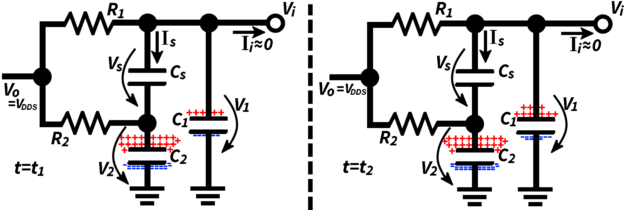
It were assumed symbolic values for the voltages on the circuit, used as specimen values to determine how fast a voltage is changing between and time moments. So for representing a small amount of electrical charge are used the symbols: [+] for positive charge and [-] for negative charge, since already stated for each additional amount of [+] and [-] charge stored on each plate (of or ) will cause an increase of capacitor voltage that will be represented as , where .
As visible in Fig.33, +4.18V, and so will eventually be the voltage on and when t. For making visual on the schematic the charging process, the charge accumulated in , was divided in 20 sets, each represented by [+], [-]; and for each set of accumulated charge is associated a corresponding increase in voltage of , and so .
Accordingly in Fig.33 is represented that is charged to near the final value () during the interval while charges much slower. During interval is visible that increased its charge only by 1[+] becoming charged to approximately(or practically) its final value(), whether is still charging and is far from its final value(), but interestingly is now increasing faster than , because already reached its final value, this is . The specimen values here mentioned are in line with the exponential function typical of capacitors charging through a resistor, where lets say a capacitor initially charges very fast, when has some charge stored it charges more slowly, and when close to being full it charges very slowly (where full means the capacitor voltage is close to power supply voltage).
4.3.1 Voltage and current specimens for
So looking at the schematic on left side of Fig.33 is visible and are charging and for the charge on is 5[+] and on is 19[+], so capacitor is almost charged while is still charging. Capacitor is charging through the path but mainly is charging through path , since then .
For , , , then , , since = then =5[]19[]=14[].
4.3.2 Voltage and current specimens for
So looking at the schematic on right side of Fig.33 is visible and are charging and for the charge on is 9[+] and on is 20[+], so capacitor is fully charged while is still charging. Capacitor is charging through the path but mainly is charging through path , since then .
For , , , then , , since = then =9[]20[]=11[].
4.3.3 Sign of as calculated from and during
The schematics in Fig.33 refer to a charging cycle of the Schmitt Trigger Oscillator. Also t0.
For [;] the capacitor is being charged through the path and so .
Also between and is = = 11[](14[])=3[], so 0 between and .
So concluding between and , , , accordingly with .
4.4 Comparison to known cases of negative capacitance
Aspects of Multiple Sensor Interface circuit possibly related to negative capacitance phenomenon:
1- Use of Schmitt-trigger ’NOT’ gate which exhibits hysteresis on its graph.
2- Multiple Sensor Interface with a capacitive sensor operates under transient(time domain), step change of voltage caused by its ’NOT’ gate(Schmitt-trigger) alternating between 0V and + (relaxation oscillator).
Negative capacitance phenomenon is reported in some scientific articles/texts, and interestingly with some coincidence to the 2 aspects mentioned above. Quotes:
1- "Effective negative capacitance has been postulated in ferroelectrics because there is hysteresis in plots of polarization-electric field.", article "Towards steep slope MOSFETs using ferroelectric negative capacitance", by A. O’Neill, year 2014 [6].
2- "The phenomenon of negative capacitance, which has been reported in a variety of situations involving electrolytic as well as electronic systems, … . It is suggested that the physically correct approach lies in the analysis of the corresponding time-domain behavior under step function bias, which involves a current initially falling and then rising gradually over a period of time before finally decaying to zero.", article "The physical origin of negative capacitance", by A. K. Jonscher, year 1986 [7].
5 Conclusions
The author theoretically demonstrated a more versatile design for use with sensor applications, also was provided experimental data that corroborates the presented theory. The motivation of the author was to make available an electronics design that could be more sustainable in terms of life-cycle duration, by making a design more customizable by the user and also not closed/locked to a specific application/purpose. No warranty is given that the design can provide accuracy or convenience to a specific application/use; as the article is focused on showing how a versatile design can be achieved.
Conflicts of interest
The author declares no conflict of interest.
Acknowledgments
I thank in general, to the Open-Source community for making available technology that everyone can use and build-on freely, thus inspiring me to also release this project as Open-Source. Also thanks to GNUplot software, that was used for drawing the plots in this article [16] .
Also thanks to Wolfram Research Inc. for providing Wolfram Mathematica® for Raspberry Pi with RaspberryPi-OS and so making their software easily available to use by everyone, it was used version 12 for obtaining/solving inverse function and algebraic manipulation of long equations [17] .
Appendix A Experimental Datasets
Experimental data obtained (Fig.5) by using fixed value components connected as the sensor on the device. Were used arrays(PCBs) with inductors, resistors, capacitors that allow to obtain various different values just by changing a jumper/switch, and also single components (including in series or parallel association).
A.1 Frequency measurement by Multi-Sensor
The Multiple-Sensor device measures frequency using a counter inside the microcontroller and has some accuracy and range limitations, it can measure up to 3MHz (higher frequency causes counter overflow). The Multiple-Sensor device was tested with a square wave signal from the signal generator JDS6600 (by Joy-IT, frequency accuracy: ppm).
The Multiple-Sensor device measurement accuracy (percentage error) of frequency, is worst at low frequencies with 9% error at 100Hz and 0.7% error at 1kHz, above 5kHz the error was always smaller than 0.2% (ignoring any accuracy error by JDS6600 used as reference). The Multiple-Sensor device measurement precision (variation) for frequency was worst at low frequencies with 5% variation at 300Hz, above 1500Hz was always smaller than 1%, and above 15kHz was always smaller than 0.1%.
A.2 Experimental data on Multi-Sensor Int
- Reference instruments:
The measurements of inductance() and capacitance() were obtained using the LCR meter TH2821A (by Tonghui, basic accuracy 0.3%), configured to 10kHz test signal (for >202mH was used 1kHz test signal).
The measurements of resistance() were obtained using the meter UT603 (by UNI-T, accuracy: 0.8% for R2M; 2% for R2M).
- Units: Hzhertz, Hhenry, ohm, Ffarad.
- Jumper Configurations:
a(JPA on, JPB off): =2.2nF; =21.8pF.
b(JPA off, JPB on): =21.8pF; =2.2nF.
c(JPA on, JPB on): =2.2nF; =2.2nF .
Here is made available, the sets of experimental data that were used for drawing the plots of , , , these are the measured values of inductance, resistance, capacitance paired with measured frequency on the Multiple Sensor Interface device.
On Appendixes A and B the symbols , , usually are/mean the same as , , and refer to measured values by the reference instruments. So on Ap. A and Ap. B, unless an explicit reference to a theoretical function is made, then =, =, =.
| Inductance | f[Hz]a JPA on, JPB off | f[Hz]b JPA off, JPB on | f[Hz]c JPA on, JPB on |
|---|---|---|---|
| 1.21 | 834161 | 879205 | 446590 |
| 1.40 | 833855 | 885138 | 476589 |
| 1.65 | 833350 | 888501 | 473393 |
| 1.85 | 833014 | 887049 | 458577 |
| 2.51 | 831302 | 881055 | 494096 |
| 3.09 | 829880 | 892844 | 474739 |
| 3.80 | 828045 | 898700 | 467354 |
| 4.10 | 827433 | 891116 | 466711 |
| 4.70 | 826011 | 881239 | 496405 |
| 5.87 | 823121 | 873380 | 519263 |
| 7.32 | 819681 | 915412 | 577595 |
| 8.76 | 813947 | 864236 | 591646 |
| 9.70 | 813397 | 858548 | 615743 |
| 11.77 | 808321 | 936894 | 1432920 |
| 12.84 | 805905 | 934723 | 1357220 |
| 15.76 | 799009 | 895932 | 1251070 |
| 21.39 | 785691 | 931940 | 1090760 |
| 24.49 | 778123 | 978330 | 1011830 |
| 31.80 | 760632 | 1056660 | 889633 |
| 38.61 | 745112 | 1193360 | 809559 |
| 46.70 | 726580 | 1369450 | 736014 |
| 53.44 | 712070 | 2853370 | 690970 |
| 61.30 | 695603 | 2662840 | 639014 |
| 78.30 | 655604 | 2332760 | 568099 |
| 95.34 | 620697 | 2103380 | 509845 |
| 117.60 | 583023 | 1899190 | 464617 |
| 142.28 | 541388 | 1722220 | 420062 |
| 173.50 | 502398 | 1575330 | 382571 |
| 201.50 | 471222 | 1464370 | 354070 |
| 271.46 | 396546 | 1201810 | 292482 |
| 341.8 | 368641 | 1112820 | 271168 |
| 360.6 | 357938 | 1085180 | 261856 |
| 438.7 | 327053 | 994721 | 239762 |
| 558.1 | 287880 | 868105 | 212362 |
| 660.7 | 262804 | 794697 | 194290 |
| 777.6 | 241031 | 737803 | 178480 |
| 921.2 | 218738 | 677591 | 163587 |
| 1491 | 161768 | 606844 | 124338 |
| 2171 | 130897 | 499264 | 102978 |
| 2976 | 109912 | 446452 | 87856 |
| 3170 | 105439 | 406011 | 84614 |
| 3640 | 97779 | 383305 | 79110 |
| 4646 | 84110 | 319423 | 69783 |
| 6880 | 68162 | 282360 | 57750 |
| 10140 | 54034 | 224090 | 47230 |
| 15040 | 43377 | 192088 | 38790 |
| 20375 | 36588 | 171981 | 33683 |
Precision error(maximum frequency variation):
2kHz (at high ’f[Hz]’); 300Hz (at low ’f[Hz]’);
5kHz (2.85MHz1.36MHz; at b JPA off, JPB on).
| [] Resistance | f[Hz]c JPA on, JPB on |
|---|---|
| 0 | 456284 |
| 1.2 | 454678 |
| 2.2 | 453975 |
| 3.2 | 453149 |
| 4.2 | 452400 |
| 5.2 | 451605 |
| 6.2 | 450718 |
| 7.2 | 449923 |
| 8.2 | 449067 |
| 9.2 | 448272 |
| 10.2 | 447385 |
| 15.2 | 443226 |
| 20.1 | 439144 |
| 25.1 | 435183 |
| 30.1 | 431269 |
| 35.1 | 427447 |
| 40.0 | 423655 |
| 45.0 | 420016 |
| 50.0 | 416407 |
| 55.0 | 412845 |
| 60.0 | 409359 |
| 65.0 | 406010 |
| 69.9 | 402601 |
| 74.9 | 399328 |
| 79.9 | 396209 |
| 84.9 | 393060 |
| 89.9 | 390017 |
| 94.8 | 387005 |
| 99.9 | 383396 |
| 119.7 | 372387 |
| 139.7 | 361700 |
| 159.6 | 351608 |
| 179.5 | 342205 |
| 199.5 | 333306 |
| 219 | 325050 |
| 239 | 317236 |
| 259 | 309836 |
| 279 | 302879 |
| 299 | 296289 |
| 319 | 290112 |
| 339 | 284225 |
| 359 | 278614 |
| 378 | 273308 |
| 398 | 268278 |
| 418 | 263462 |
| 438 | 258829 |
| 458 | 254471 |
| 478 | 250251 |
| 498 | 246214 |
| 518 | 242361 |
| 538 | 238646 |
| 557 | 235144 |
| [] Resistance | f[Hz]c JPA on, JPB on |
|---|---|
| 577 | 231735 |
| 597 | 228447 |
| 617 | 225252 |
| 637 | 222178 |
| 657 | 219228 |
| 677 | 216353 |
| 697 | 213647 |
| 717 | 210971 |
| 736 | 208402 |
| 756 | 205910 |
| 776 | 203464 |
| 796 | 201139 |
| 816 | 198877 |
| 836 | 196659 |
| 856 | 194504 |
| 876 | 192409 |
| 896 | 190406 |
| 916 | 188418 |
| 936 | 186476 |
| 955 | 184611 |
| 975 | 182776 |
| 996 | 180865 |
| 1096 | 172578 |
| 1195 | 165208 |
| 1295 | 158603 |
| 1394 | 152594 |
| 1494 | 147150 |
| 1593 | 142135 |
| 1693 | 137548 |
| 1792 | 133298 |
| 1892 | 129353 |
| 1992 | 125699 |
| 2090 | 122258 |
| 2190 | 119017 |
| 2290 | 115974 |
| 2390 | 113115 |
| 2490 | 110409 |
| 2590 | 107855 |
| 2690 | 105424 |
| 2790 | 103115 |
| 2890 | 100914 |
| 2990 | 98819 |
| 3090 | 96831 |
| 3190 | 94905 |
| 3290 | 93070 |
| 3390 | 91327 |
| 3490 | 89645 |
| 3580 | 88024 |
| 3680 | 86464 |
| 3780 | 84966 |
| 3880 | 83529 |
| 3980 | 82153 |
| [] Resistance | f[Hz]c JPA on, JPB on |
|---|---|
| 4180 | 79553 |
| 4380 | 77107 |
| 4580 | 74783 |
| 4780 | 72612 |
| 4980 | 70593 |
| 5180 | 68682 |
| 5380 | 66863 |
| 5580 | 65135 |
| 5770 | 63514 |
| 5970 | 61985 |
| 6170 | 60517 |
| 6370 | 59111 |
| 6570 | 57765 |
| 6770 | 56511 |
| 6970 | 55288 |
| 7170 | 54126 |
| 7370 | 53010 |
| 7570 | 51940 |
| 7760 | 50915 |
| 7960 | 49952 |
| 8460 | 47643 |
| 8960 | 45548 |
| 9460 | 43622 |
| 9960 | 41879 |
| 10460 | 40243 |
| 10960 | 38760 |
| 11460 | 37353 |
| 11960 | 36053 |
| 12450 | 34861 |
| 12960 | 33714 |
| 13450 | 32659 |
| 13950 | 31680 |
| 14450 | 30732 |
| 14950 | 29861 |
| 15440 | 29035 |
| 15940 | 28255 |
| 16440 | 27522 |
| 16940 | 26818 |
| 17430 | 26145 |
| 17930 | 25503 |
| 18430 | 24907 |
| 18930 | 24326 |
| 19420 | 23775 |
| 19940 | 23271 |
| 20900 | 22292 |
| 21900 | 21375 |
| 22900 | 20549 |
| 23900 | 19769 |
| 24900 | 19066 |
| 25900 | 18393 |
| 26900 | 17782 |
| 27900 | 17201 |
| [] Resistance | f[Hz]c JPA on, JPB on |
|---|---|
| 28900 | 16666 |
| 29900 | 16176 |
| 31900 | 15244 |
| 33900 | 14418 |
| 35900 | 13669 |
| 37800 | 13027 |
| 39800 | 12430 |
| 41800 | 11880 |
| 43800 | 11375 |
| 45800 | 10917 |
| 47800 | 10488 |
| 49800 | 10091 |
| 54800 | 9235 |
| 59800 | 8531 |
| 64800 | 7904 |
| 69700 | 7385 |
| 74700 | 6926 |
| 79700 | 6513 |
| 84600 | 6146 |
| 89600 | 5825 |
| 94600 | 5550 |
| 99400 | 5320 |
| 109400 | 4862 |
| 119300 | 4479 |
| 129300 | 4158 |
| 139300 | 3883 |
| 149300 | 3623 |
| 159200 | 3440 |
| 169200 | 3256 |
| 179100 | 3073 |
| 189100 | 2935 |
| 199100 | 2798 |
| 299000 | 1972 |
| 398000 | 1544 |
| 498000 | 1284 |
| 597000 | 1100 |
| 697000 | 978 |
| 796000 | 886 |
| 896000 | 825 |
| 995000 | 779 |
| 1495000 | 596 |
| 1993000 | 504 |
| 2490000 | 458 |
| 3090000 | 412 |
| 4080000 | 366 |
| 5080000 | 351 |
| 6070000 | 336 |
| 7070000 | 321 |
| 8050000 | 321 |
| 9040000 | 305 |
Precision error(maximum frequency variation):
1kHz(at low ); 300Hz(at 30k); 100Hz(at high ).
| [nF] Capacitance | f[Hz]c JPA on, JPB on |
|---|---|
| 0 | 229 |
| 0.152 | 321 |
| 0.310 | 458 |
| 0.568 | 2614 |
| 0.615 | 54570 |
| 0.689 | 110286 |
| 0.776 | 140178 |
| 1.015 | 186522 |
| 1.34 | 231460 |
| 1.58 | 255526 |
| 1.79 | 271015 |
| 2.00 | 285020 |
| 2.56 | 314530 |
| 2.99 | 329820 |
| 3.98 | 356012 |
| [nF] Capacitance | f[Hz]c JPA on, JPB on |
|---|---|
| 4.97 | 373045 |
| 5.97 | 385032 |
| 6.95 | 394283 |
| 7.94 | 400750 |
| 8.98 | 405766 |
| 10.07 | 411246 |
| 12.04 | 418028 |
| 15.02 | 426040 |
| 20.02 | 433089 |
| 24.97 | 437446 |
| 29.68 | 440382 |
| 34.62 | 442584 |
| 39.43 | 444235 |
| 44.38 | 445688 |
| 49.38 | 446712 |
Precision error(maximum frequency variation):
3kHz (600pF1.6nF); 1kHz (21nF);
2kHz (1.6nF21nF); 50Hz (600pF).
Appendix B Additional Experimental Datasets
Here are additional experimental datasets, these are measured values of inductance, resistance, capacitance paired with measured frequency by the Multi-Sensor device. These additional experimental datasets were not used on any previous plot/graph displayed along the article, and are here made available to give additional evidence, also with graphs comparing them against the respective theoretical results. The symbols , , are/mean the same as on Appendix A.
- Reference instruments: Same as on Appendix A.
- Jumper Configurations/Capacitor Values:
d(JPA on, JPB off): =93nF (91nF+2.2nF); =21.8pF.
e(JPA off, JPB on): =21.8pF; =93nF (91nF+2.2nF).
f(JPA on, JPB on): =93nF; =93nF (91nF+2.2nF).
- Note: The configurations/designs where the references and/or are 93nF(91nF//2.2nF=91nF+2.2nF), were obtained by connecting a 91nF capacitor in parallel with the 2.2nF capacitor already on the Multi-Sensor PCB.
The Fig.34 shows experimental data for Multi-Sensor device with various resistance values connected as the sensor and also using (9) with , , , , , , .

The Fig.36 and Fig.36 shows experimental data for Multi-Sensor device with various capacitance values connected as sensor and using (17) with , , , , , , .


The Fig.38 and Fig.38 shows experimental data for Multiple-Sensor device with various inductance values connected as the sensor, and also using (34) with =93nF, =21.78pF, , , , ==0.5, ==0.01, , .


| [] Resistance | f[Hz]f JPA on, JPB on |
|---|---|
| 0.1 | 10198 |
| 1.2 | 10183 |
| 2.2 | 10167 |
| 3.2 | 10152 |
| 4.2 | 10137 |
| 5.2 | 10106 |
| 6.2 | 10091 |
| 7.2 | 10076 |
| 8.2 | 10045 |
| 9.2 | 10030 |
| 10.2 | 10014 |
| 15.2 | 9923 |
| 20.1 | 9816 |
| 25.1 | 9724 |
| 30.1 | 9632 |
| 35.1 | 9540 |
| 40.0 | 9449 |
| 45.0 | 9357 |
| 50.0 | 9281 |
| 55.0 | 9204 |
| 60.0 | 9128 |
| 65.0 | 9036 |
| 69.9 | 8944 |
| 74.9 | 8883 |
| 79.9 | 8807 |
| 84.9 | 8715 |
| 89.9 | 8669 |
| 94.8 | 8577 |
| 99.9 | 8485 |
| 119.7 | 8210 |
| 139.7 | 7966 |
| 159.6 | 7736 |
| 179.5 | 7522 |
| 199.5 | 7293 |
| 219 | 7109 |
| 239 | 6926 |
| 259 | 6758 |
| 279 | 6605 |
| 299 | 6467 |
| 319 | 6314 |
| 339 | 6192 |
| 359 | 6054 |
| 378 | 5932 |
| 398 | 5825 |
| 418 | 5718 |
| 438 | 5611 |
| 458 | 5504 |
| 478 | 5412 |
| 498 | 5320 |
| 518 | 5229 |
| 538 | 5152 |
| 557 | 5091 |
| [] Resistance | f[Hz]f JPA on, JPB on |
|---|---|
| 577 | 4999 |
| 597 | 4923 |
| 617 | 4862 |
| 637 | 4785 |
| 657 | 4724 |
| 677 | 4663 |
| 697 | 4587 |
| 717 | 4541 |
| 736 | 4479 |
| 756 | 4418 |
| 776 | 4357 |
| 796 | 4311 |
| 816 | 4265 |
| 836 | 4220 |
| 856 | 4174 |
| 876 | 4128 |
| 896 | 4082 |
| 916 | 4036 |
| 936 | 3990 |
| 955 | 3944 |
| 975 | 3898 |
| 996 | 3868 |
| 1096 | 3700 |
| 1195 | 3531 |
| 1295 | 3394 |
| 1394 | 3256 |
| 1494 | 3134 |
| 1593 | 3027 |
| 1693 | 2935 |
| 1792 | 2843 |
| 1892 | 2752 |
| 1992 | 2675 |
| 2090 | 2614 |
| 2190 | 2522 |
| 2290 | 2476 |
| 2390 | 2400 |
| 2490 | 2339 |
| 2590 | 2293 |
| 2690 | 2247 |
| 2790 | 2201 |
| 2890 | 2155 |
| 2990 | 2110 |
| 3090 | 2064 |
| 3190 | 2018 |
| 3290 | 1972 |
| 3390 | 1941 |
| 3490 | 1911 |
| 3580 | 1880 |
| 3680 | 1834 |
| 3780 | 1804 |
| 3880 | 1788 |
| 3980 | 1743 |
| [] Resistance | f[Hz]f JPA on, JPB on |
|---|---|
| 4180 | 1697 |
| 4380 | 1651 |
| 4580 | 1590 |
| 4780 | 1544 |
| 4980 | 1513 |
| 5180 | 1467 |
| 5380 | 1421 |
| 5580 | 1376 |
| 5770 | 1345 |
| 5970 | 1330 |
| 6170 | 1284 |
| 6370 | 1253 |
| 6570 | 1223 |
| 6770 | 1192 |
| 6970 | 1162 |
| 7170 | 1146 |
| 7370 | 1131 |
| 7570 | 1100 |
| 7760 | 1085 |
| 7960 | 1055 |
| 8460 | 1009 |
| 8960 | 963 |
| 9460 | 917 |
| 9960 | 871 |
| 10460 | 856 |
| 10960 | 825 |
| 11460 | 779 |
| 11960 | 764 |
| 12450 | 733 |
| 12960 | 703 |
| 13450 | 688 |
| 13950 | 672 |
| 14450 | 642 |
| 14950 | 626 |
| 15440 | 611 |
| 15940 | 596 |
| 16440 | 581 |
| 16940 | 565 |
| 17430 | 550 |
| 17930 | 535 |
| 18430 | 519 |
| 18930 | 504 |
| 19420 | 504 |
| 19940 | 489 |
| 20900 | 458 |
| 21900 | 443 |
| 22900 | 428 |
| 23900 | 412 |
| 24900 | 397 |
| 25900 | 382 |
| 26900 | 366 |
| 27900 | 351 |
| [] Resistance | f[Hz]f JPA on, JPB on |
|---|---|
| 28900 | 336 |
| 29900 | 336 |
| 31900 | 321 |
| 33900 | 290 |
| 35900 | 275 |
| 37800 | 275 |
| 39800 | 259 |
| 41800 | 244 |
| 43800 | 229 |
| 45800 | 229 |
| 47800 | 214 |
| 49800 | 198 |
| 54800 | 183 |
| 59800 | 168 |
| 64800 | 152 |
| 69700 | 137 |
| 74700 | 137 |
| 79700 | 137 |
| 84600 | 122 |
| 89600 | 122 |
| 94600 | 107 |
| 99400 | 91 |
| 109400 | 91 |
| 119300 | 91 |
| 129300 | 76 |
| 139300 | 76 |
| 149300 | 61 |
| 159200 | 61 |
| 169200 | 45 |
| 179100 | 45 |
| 189100 | 45 |
| 199100 | 45 |
| 299000 | 30 |
| 398000 | 15 |
| 498000 | 15 |
| 597000 | 0 |
| 697000 | 0 |
| 796000 | 0 |
| 896000 | 0 |
| 995000 | 0 |
| 1495000 | 0 |
| 1993000 | 0 |
| 2490000 | 0 |
| 3090000 | 0 |
| 4080000 | 0 |
| 5080000 | 0 |
| 6070000 | 0 |
| 7070000 | 0 |
| 8050000 | 0 |
| 9040000 | 0 |
Precision error(maximum frequency variation):
300Hz(at low ); 50Hz(at 996); 30Hz(at high ).
| Inductance | f[Hz]d JPA on, JPB off , | f[Hz]e JPA off, JPB on , | f[Hz]f JPA on, JPB on , |
|---|---|---|---|
| 1.21 | 20458 | 20503 | 10259 |
| 1.85 | 20412 | 20519 | 10259 |
| 3.09 | 20412 | 20488 | 10259 |
| 4.70 | 20442 | 20503 | 10259 |
| 7.32 | 20458 | 20503 | 10259 |
| 9.70 | 20442 | 20519 | 10244 |
| 15.76 | 20458 | 20503 | 10259 |
| 21.39 | 20472 | 20503 | 10244 |
| 24.49 | 20458 | 20503 | 10274 |
| 38.61 | 20396 | 20503 | 10229 |
| 46.70 | 20366 | 20503 | 10274 |
| 53.44 | 20335 | 20503 | 10320 |
| 61.30 | 20320 | 20503 | 10091 |
| 78.30 | 20274 | 20503 | 10473 |
| 95.34 | 20228 | 20503 | 9984 |
| 117.60 | 20182 | 20534 | 10473 |
| 142.28 | 20106 | 20503 | 10488 |
| 173.50 | 20045 | 20503 | 9892 |
| 201.50 | 19968 | 20534 | 9907 |
| 271.46 | 19815 | 20427 | 10917 |
| 341.8 | 19647 | 20503 | 10229 |
| 360.6 | 19555 | 20595 | 10045 |
| 438.7 | 19403 | 20565 | 10657 |
| 558.1 | 19143 | 20519 | 10366 |
| 660.7 | 18944 | 20626 | 9724 |
| 777.6 | 18699 | 20503 | 9128 |
| 921.2 | 18439 | 20503 | 8669 |
| 1491 | 17614 | 20687 | 18072 |
| 2171 | 16452 | 20763 | 14877 |
| 2976 | 15259 | 20595 | 12751 |
| 3170 | 14877 | 20779 | 12109 |
| 3640 | 14219 | 20549 | 11284 |
| 4646 | 13684 | 20870 | 9953 |
| 6880 | 11758 | 20779 | 8394 |
| 10140 | 9953 | 20213 | 6972 |
| 15040 | 7721 | 20962 | 5764 |
| 20375 | 6941 | 20580 | 4923 |
| 33370 | 5412 | 20794 | 3853 |
| 68050 | 3715 | 23286 | 2752 |
| 102950 | 2935 | 63744 | 2247 |
| 136900 | 2522 | 62276 | 1941 |
| 202650 | 2064 | 43408 | 1651 |
| 269650 | 1804 | 37888 | 1452 |
| 358300 | 1513 | 21100 | 1162 |
| 532200 | 1238 | 21008 | 1009 |
| 684100 | 1024 | 20870 | 825 |
Precision error(maximum frequency variation):
300Hz (at high ’f[Hz]’); 100Hz (at low ’f[Hz]’);
2kHz ([37888Hz;63744Hz]; at e JPA off, JPB on).
| [nF] Capacitance | f[Hz]f JPA on, JPB on |
|---|---|
| 0.152 | 0 |
| 0.568 | 0 |
| 1.015 | 0 |
| 1.58 | 0 |
| 2.00 | 0 |
| 2.99 | 0 |
| 3.98 | 0 |
| 4.97 | 0 |
| 5.97 | 0 |
| 7.94 | 0 |
| 10.07 | 0 |
| 12.04 | 0 |
| 15.02 | 0 |
| 20.02 | 0 |
| 24.97 | 30 |
| 25.89 | 45 |
| 26.87 | 107 |
| 27.86 | 1055 |
| 28.87 | 1605 |
| 29.68 | 1850 |
| 34.62 | 2782 |
| 39.43 | 3363 |
| 44.38 | 3853 |
| [nF] Capacitance | f[Hz]f JPA on, JPB on |
|---|---|
| 49.38 | 4235 |
| 59.39 | 4908 |
| 69.62 | 5443 |
| 79.96 | 5871 |
| 90.38 | 6223 |
| 100.38 | 6513 |
| 120.27 | 6972 |
| 139.62 | 7339 |
| 159.66 | 7629 |
| 180.22 | 7889 |
| 201.13 | 8103 |
| 250.42 | 8470 |
| 300.0 | 8730 |
| 349.3 | 8944 |
| 400.2 | 9097 |
| 502.9 | 9311 |
| 603.7 | 9495 |
| 706.7 | 9586 |
| 806.5 | 9678 |
| 909.1 | 9755 |
| 1003.5 | 9800 |
| 1507.3 | 9953 |
| 1991.7 | 10045 |
Precision error(maximum frequency variation):
15Hz (34.62nF); 50Hz (100.38nF180.22nF);
30Hz (34.62nF100.38nF); 100Hz (180.22nF).
Appendix C Abbreviations
| ADC | Analog to Digital Converter |
| CC BY-NC-SA | Creative Commons, Attribution - NonCommercial - ShareAlike |
| CERN | Conseil Europeen pour la Recherche Nucleaire |
| CERN-OHL-W |
CERN Open Hardware Licence
- Weakly reciprocal |
| CMOS | Complementary Metal Oxide Semiconductor |
| EEPROM | Electrically Erasable Programmable Read-Only Memory |
| ESD-safe foam | Electrostatic Sensitive Device safe foam |
| FSR | Force Sensitive Resistor (sensor) |
| GND | Ground (voltage reference) |
| GPIO | General-Purpose Input/Output |
| LDR | Light Dependent Resistor (sensor) |
| OCR | Optical Character Recognition |
| PCB | Printed Circuit Board |
| PWM | Pulse-Width Modulation |
| QR-code | Quick Response code |
| RS-485 |
Recommended Standard 485
(aka. EIA/TIA-485) |
| RTD | Resistance Temperature Detector (sensor) |
| UART | Universal Asynchronous Receiver-Transmitter |
| USB | Universal Serial Bus |
| VDD | Voltage Supply (Voltage Drain Drain) |
| VDDS | VDD Stabilized |
Appendix D LDR Sensor Calibration Dataset
The A906013 LDR sensor has the following electrical parameters specified by the manufacturer(PerkinElmer/Excelitas):
R(Illum=10[lx]) is between 27k (min.) and 94k (max.); R(Illum=100[lx]) = 8k (typical value) ;
=600nm ( is the wavelength of light the LDR sensor is most sensitive to); R(Illum=0, after 1s)<0.5M ;
R(Illum=0, after 5s)<1.5M .
- Reference instruments:
For obtaining the calibration table of the A906013 LDR sensor on the Multiple-Sensor device it was used as a reference device the Mastech MS6610 luxmeter; the MS6610 luxmeter has the maximum sensitivity at 570nm wavelength, it has an accuracy of , with a resolution (value per digit) of: [0; 1999 [lx]]: 1 [lx]; [2000 [lx]; 19990 [lx]]: 10 [lx]; [20000 [lx]; 50000 [lx]]: 100 [lx].
- Jumper Configurations:
c(JPA on, JPB on): =2.2nF; =2.2nF .
- Units: Hzhertz, lxlux.
Here is made available the calibration of a LDR sensor (Ref: A906013) connected on the Multiple-Sensor Interface.
| [lx] ref. MS6601 | f[Hz]c (LDR) JPA on, JPB on |
|---|---|
| 0 | 244 |
| 1 | 2507 |
| 3 | 6284 |
| 10 | 11788 |
| 15 | 16345 |
| 25 | 23026 |
| 30 | 25320 |
| 48 | 32644 |
| 77 | 44172 |
| 100 | 49768 |
| 122 | 56404 |
| 145 | 63835 |
| 173 | 67346 |
| 205 | 75456 |
| 251 | 81847 |
| 300 | 90180 |
| 398 | 102580 |
| 450 | 107641 |
| 512 | 113375 |
| 590 | 120378 |
| 650 | 124032 |
| 715 | 129124 |
| 820 | 135591 |
| 925 | 141218 |
| 1072 | 147105 |
| 1200 | 155682 |
| 1365 | 162196 |
| [lx] ref. MS6601 | f[Hz]c (LDR) JPA on, JPB on |
|---|---|
| 1485 | 165972 |
| 1660 | 173663 |
| 1880 | 189030 |
| 1985 | 193433 |
| 2160 | 198678 |
| 2400 | 205650 |
| 2930 | 217530 |
| 3950 | 232041 |
| 5000 | 244640 |
| 6000 | 252651 |
| 6950 | 261810 |
| 8100 | 267620 |
| 9650 | 275877 |
| 11000 | 281121 |
| 12050 | 286595 |
| 13350 | 291702 |
| 15500 | 297130 |
| 17250 | 300846 |
| 19000 | 305205 |
| 22600 | 311227 |
| 25600 | 315707 |
| 28600 | 319469 |
| 30300 | 320891 |
| 33400 | 325050 |
| 37000 | 328750 |
| 39800 | 333459 |
| 48000 | 340600 |
Precision error(maximum frequency variation):
3kHz (1k[lx]10k[lx]); 6kHz (10k[lx]);
1kHz (10[lx]1k[lx]); 200Hz (10[lx])
References
- [1]
- [2] Peter McLean, (2020). Topic 4 - Crystal Oscillators (Pierce oscillator analysis) - Digital Electronics (UTS-AU). Accessed July 2021. https://pmcl.net.au/de .
- [3] R.C. Jaeger, T.N. Blalock, (2011). Microelectronic Circuit Design (4th ed.); McGraw–Hill. - ’18.6.1 THE COLPITTS OSCILLATOR’ p. 1278, ’18.6.6 CRYSTAL OSCILLATORS’ pp. 1283-1285, ’C.2 THE HYBRID OR h-PARAMETERS (Appendix C)’ p. 1311 .
- [4] A. S. Sedra, K. C. Smith, T. C. Carusone, V. Gaudet, (2021). Microelectronic Circuits (8th inte. ed.); Oxford University Press. - "13.11 LC and Crystal Oscillators" - pp. 1044-1052 .
-
[5]
Eduardo Corpeno - AllAboutCircuits (2018). Exactly How Schmitt Trigger Oscillators Work.
Accessed July 2021.
https://www.allaboutcircuits.com/technical-articles/exactly-how-schmitt-trigger-oscillators-work . - [6] A. O’Neill, D. Appleby, N. Ponon, K. Kwa, (2015). Towards steep slope MOSFETs using ferroelectric negative capacitance. 2014 12th IEEE International Conference on Solid-State and Integrated Circuit Technology (ICSICT). DOI: 10.1109/ICSICT.2014.7021281 .
- [7] Andrew K. Jonscher, (1986). The physical origin of negative capacitance. J. Chem. Soc., Faraday Trans. 2, vol. 82, no. 1, pp. 75-81. DOI: 10.1039/F29868200075 .
- [8] S. N. Nihtianov, G. P. Shterev, B. Iliev, G. C. M. Meijer, (2001). An interface circuit for R-C impedance sensors with a relaxation oscillator. IEEE Transactions on Instrumentation and Measurement, vol. 50, no. 6, pp. 1563-1567, DOI: 10.1109/19.982945 .
- [9] J. H. Lu, M. Inerowicz, S. Joo, J. Kwon, B. Jung, (2011). A Low-Power, Wide-Dynamic-Range Semi-Digital Universal Sensor Readout Circuit Using Pulsewidth Modulation. IEEE Sensors Journal, vol. 11, no. 5, pp. 1134-1144. DOI: 10.1109/JSEN.2010.2085430 .
- [10] F.M.L.v.d. Goes, G.C.M. Meijer, (1997). A Universal Transducer Interface for Capacitive and Resistive Sensor Elements. Analog Integrated Circuits and Signal Processing 14, pp. 249–260. DOI: 10.1023/A:1008246103915 .
- [11] Xiaowen Liu, D. Rairigh, Chao Yang, A. J. Mason, (2009). Impedance-to-digital converter for sensor array microsystems, 2009 IEEE International Symposium on Circuits and Systems (ISCAS), pp. 353-356, DOI: 10.1109/ISCAS.2009.5117758 .
- [12] V. Dumbrava, L. Svilainis, (2007). The Automated Complex Impedance Measurement System. Elektronika Ir Elektrotechnika, 76(4), pp. 59-62. https://eejournal.ktu.lt/index.php/elt/article/view/10720
- [13] HIOKI website, (2021). LCR meter basic measurement principles. Accessed December 2021. https://www.hioki.com/global/learning/usage/lcr-meters_1.html .
- [14] H. Bi, K. Yin, X. Xie, J. Ji, S. Wan, L. Sun, M. Terrones, M. S. Dresselhaus, (2013). Ultrahigh humidity sensitivity of graphene oxide. Scientific Reports 2013;3:2714. DOI: 10.1038/srep02714 .
- [15] C. Yang, A. Mason, J. Xi, P. Zhong, (2006). Configurable Hardware-Efficient Interface Circuit for Multi-Sensor Microsystems. SENSORS 2006 IEEE, pp. 41-44. DOI: 10.1109/ICSENS.2007.355713 .
- [16] Thomas Williams, Colin Kelley (2007) - GNUplot software. Accessed July 2021. http://gnuplot.sourceforge.net .
- [17] Wolfram Research, Inc. - Wolfram Mathematica 12 for Raspberry Pi. 2022. https://www.wolfram.com/raspberry-pi .