Terahertz rectennas on flexible substrates based on one-dimensional metal-insulator-graphene diodes
Abstract
Flexible energy harvesting devices fabricated in scalable thin-film processes are important components in the field of wearable electronics and the Internet of Things. We present a flexible rectenna based on a one-dimensional junction metal-insulator-graphene diode, which offers low-noise power detection at terahertz (THz) frequencies. The rectennas are fabricated on a flexible polyimide film in a scalable process by photolithography using graphene grown by chemical vapor deposition. A one-dimensional junction area reduces the junction capacitance and enables operation in the D-band (110 - 170 GHz). The rectenna on polyimide shows a maximum voltage responsivity of 80 V/W at 167 GHz in free space measurements and minimum noise equivalent power of 80 pW/.
Chair of Electronic Devices, Faculty of Electrical Engineering and Information Technology, RWTH Aachen University, Otto-Blumenthal-Str. 2, 52074 Aachen, Germany \alsoaffiliationChair of Electronic Devices, Faculty of Electrical Engineering and Information Technology, RWTH Aachen University, Otto-Blumenthal-Str. 2, 52074 Aachen, Germany \alsoaffiliationChair of Electronic Devices, Faculty of Electrical Engineering and Information Technology, RWTH Aachen University, Otto-Blumenthal-Str. 2, 52074 Aachen, Germany \alsoaffiliationAdvanced Microelectronic Center Aachen (AMICA), AMO GmbH, Otto-Blumenthal-Str. 25, 52074 Aachen, Germany \mciteErrorOnUnknownfalse

Terahertz (THz) radiation is a region of the electromagnetic spectrum with frequencies between 0.1 and 10 THz 1, 2, 3.
Miniaturized THz sources and detectors enable a variety of applications, such as communications, surveillance screening, material analysis, biomedical diagnostics and personal healthcare tracking 1, 2, 4, 5.
The emergence of wearable electronics and networks of small, independent sensors for Internet of Things (IoT) applications is driving research both in low power electronic circuits and in energy harvesting on the device or chip level.
Miniaturized THz power detectors may become crucial components that can function as energy harvesting devices, in particular on flexible thin-film substrates, where they can overcome the form factor limitations of silicon (Si) electronic chips and can be fabricated in scalable roll-to-roll processes.
Thus, they have the potential to power decentralized sensor networks, passive readout circuits or integrated mobile devices without the need for batteries or an external power supply 6.
Rectennas - antenna-coupled diodes - are versatile two-terminal devices that directly rectify a detected signal.
Their zero-bias operation makes them suitable for energy harvesting applications 7, 8.
This principle has been well established in the microwave region since 1966 9, due to the availability of Schottky diodes with sufficiently short response times 10, 11, 12, 13.
Increased cutoff frequencies in the THz range 14 have been achieved by metal-insulator-metal (MIM) diodes, which utilize tunneling and thermionic majority carrier conduction.
However, MIM diodes generally show inferior DC performance compared to conventional p-n junction or Schottky diodes 15, 16.
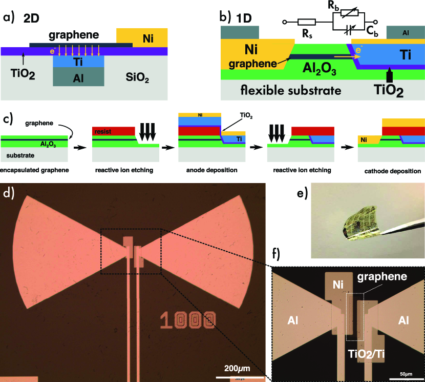
Metal-insulator-graphene (MIG) diodes (Figure 1a), where the cathode
metal of a MIM diode is replaced by graphene, combine excellent DC performance with high cutoff frequencies 15, 17, 18, 19.
The high charge carrier mobility and flexibility of graphene 19 allow such devices to be used in flexible THz rectennas, an application space that has been inaccessible due to the rigidity, bias and fabrication requirements of conventional semiconductor-based detectors.
We present rectennas based on edge-contacted MIG diodes (Figure 1b), fabricated in a scalable thin-film compatible process, enabling high-throughput fabrication.
The results point towards the possibility to integrate rectenna arrays as power supplies in flexible, wearable and conformal devices, for example wearable biomedical or distributed environmental sensors.
The operation frequency of a diode can be estimated using:
| (1) |
where is the access resistance and is the barrier capacitance from the diode’s equivalent circuit seen in Figure 1b 19, 20.
The low access resistance of conventional MIM diodes allows them to reach very high cutoff frequencies in the THz range, however with rather poor rectification performance 15.
MIG diodes, which have a similar layout as MIM diodes (Figure 1a), offer better rectification, but at the expense of a larger access resistance and therefore lower operation speed, as one metal layer is replaced by graphene.
Furthermore, the current through a two-dimensional (2D) MIG diode is emitted perpendicularly to the graphene plane across a small ”van-der-Waals gap” and is therefore affected by surface species at the graphene-insulator interface.
This can increase the junction resistance, hindering an efficient coupling between antenna and diode18.
By forming a one-dimensional (1D) diode junction only to the graphene edge, as shown in the schematic cross section in Figure 1b, the junction capacitance can be significantly reduced, enabling operation frequencies up to the THz range 21.
The effective junction area is then given by , where is the channel width and is the thickness of graphene, about 0.3 nm 22.
This leads simultaneously to a reduced junction capacitance (), improved current injection at the insulator-graphene and graphene-metal interfaces and reduced operating voltage due to the electric field enhancement at the 1D edge 21.
The rectennas consist of edge-contacted metal-insulator-graphene diodes at the feedpoint of broadband bowtie antennas.
The rectennas have been fabricated on THz-transparent polyimide (PI) films on silicon handling substrates using standard microprocessing techniques such as contact photolithography and reactive ion etching.
Key fabrication steps are shown in Figure 1c.
The PI has first been covered with an aluminum oxide (\chAl2O3) layer through plasma-enhanced atomic layer deposition (ALD).
CVD-grown graphene has been transferred in a wet process 23 onto the substrate and encapsulated with 20 nm \chAl2O3 in a thermal ALD process.
A photolithographically defined mask has been used for reactive ion etching (RIE) through the \chAl2O3 and the graphene. The resist remains on the chip at this point and acts as a lift-off mask for the subsequent atomic layer deposition of 5 nm \chTiO2 insulator, 20 nm sputtered titanium (Ti) anode metal 18, 19 and 13 nm nickel (Ni). The self-aligned nature of the process prevents contamination of the graphene edge from photoresist residues or misalignment of graphene and metal layers, which would increase the diodes’ capacitance and resistance. This process results in a one-dimensional MIG junction, because only the graphene edge is in electrical contact with the \chTiO2 barrier (Figure 1b), as opposed to the two-dimensional contact in conventional MIG stacks (Figure 1a).
A 25 nm thick Ni contact to the graphene has been fabricated in a similar way, i.e. by reactive ion etching through the \chAl2O3/graphene/\chAl2O3 stack and subsequent metal deposition.
Here, the graphene edge is in direct contact with the Ni and forms an ohmic contact 19, 24, 25.
At this point, graphene still covers the entire chip apart from directly below both metal contacts.
The remaining graphene has been patterned into 6 long and 50 wide channels, before 100 nm thick aluminum (Al) has been deposited as antennas, transmission lines and contact pads.
A key feature of the presented metal-insulator-graphene rectenna is that it is compatible with conventional thin-film technologies, i.e. it does not involve high temperature processing steps 300∘C and uses only m-scale lithography.
A micrograph of a fabricated rectenna is shown in Figure 1d. The polyimide film is removed from the Si carrier substrate after the device fabrication for electrical measurements. Figure 1e shows a flexible PI substrate with several THz rectennas. A close-up of the finished diode on a flexible substrate is shown in Figure 1f.
The transmission behavior of the antennas was designed for broadband absorption to match the measurement setup tailored to the D band from 110 to 170 GHz.
The parameter space was modeled using the electromagnetic finite element solver HFSS with a lumped port ( = 377 ) at the feedpoint.
The chosen bowtie antenna design with an opening angle of 30∘ has a large bandwidth of 43% at 157 GHz (defined as a voltage standing wave ratio VSWR 2), enabling free space measurements over the D band from 110 to 170 GHz.
A pair of 1 mm long metal traces lead from the diode contacts to larger contact pads for biasing and signal readout.
The transmission line serves as a low-pass filter that rejects the received THz signal and only allows the rectified DC component to pass.

Direct current (DC) characteristics of the rectennas have been measured under ambient conditions.
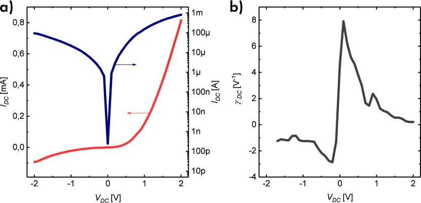
Current-voltage (-) measurements, where the bias voltage has been swept from -2 to +2 V, are shown linearly and logarithmically in Figure 2a. The device shows a non-linear - characteristic and reaches maximum currents of mA at a forward bias voltage of V and mA at V.
Typically, such currents are normalized by the device dimensions in order to compare them to the state of the art.
Here, only the graphene edge emits charge carriers across the barrier.
Taking into account the graphene thickness of approximately 0.3 nm and the device width of 50 µm, the resulting maximum current density at the graphene edge exceeds A/cm2 in the forward direction, consistent with previously reported 1D-MIG diodes by Wang et al. 19.
The - curve allows calculating the responsivity of the diode, one of the decisive figures of merit for RF applications. The responsivity is a measure for the rectification efficiency of the diode 18:
| (2) |
As can be seen from its expanded units (), a diode’s responsivity is related to the rectified current at a given input power.
The flexible diode reaches a maximum responsivity of 8 V-1 (Figure 2b) in the vicinity of V.

Measurements at THz frequencies between 110 and 170 GHz were conducted in free space under ambient conditions.
A sine-wave modulated THz signal (333 Hz) was transmitted by a horn antenna, collimated and prefocused by two identical PTFE (Teflon) lenses and finally focused onto the back of the sample by a hyper-hemispherical Si lens.
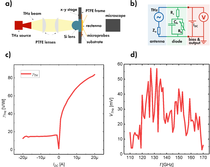
The setup is shown schematically in Figure 3a.
After peeling off the PI film from the Si substrate, the flexible chip was mounted onto a high-resistivity Si lens in the beam path.
Microprobes contacted the sample behind the beam path.
A Keithley 2604B source meter provided the DC input bias as a current through an external resistor and simultaneously measured the DC voltage at the diode.
The THz source was composed of a VDI WR6.5GX extender driven by an Agilent 83650A signal generator with 30 dB sine wave modulation at 333 Hz.
The rectified voltage response was measured using an SR830 lock-in amplifier.
For calibration, the available output power of the extender across the D band was measured using an Erickson calorimetric power meter directly at the waveguide flange of the extender on which the horn antenna was mounted.
To describe the diode’s behavior during THz measurement we formulate a small-signal equivalent circuit, shown in Figure 3b.
A key THz detector characteristic is the optical voltage responsivity , which is defined in Eq. 3 as the DC output voltage per THz power and is given in units of [V/W]:
| (3) |
Here, is the rectified DC voltage measured by the lock-in amplifier 26.
The optical current responsivity in [A/W] can be calculated from the voltage responsivity and the total diode resistance at the respective operating point.
The pre-factors originate in the peak-to-peak and root mean square (rms) amplitudes of the lock-in amplifier 26. The bias-dependent THz response was measured at 167 GHz with a THz output power .
The maximum optical voltage responsivity was reached at an applied bias current of 20 µA and a measured DC voltage of 1.47 V (Figure 3c).
This corresponds to an optical current responsivity at a total device resistance .
It is noticeable that the optical responsivity under THz measurements increases with applied bias, while the DC responsivity shows a peak close to zero bias.
This can be explained by the non-ideal impedance matching between diode and antenna.
As a higher bias is applied, the junction resistance of the diode decreases, thus better matching its impedance to that of the antenna, and increasing the power delivered to the diode.
The rectified voltage over the D band from 110 to 170 GHz is shown in Figure 3d.
During the frequency sweep the bias current was fixed at -10 µA and the rectified voltage was recorded.
The voltage does not show any noticeable frequency dependency, but fluctuations, possibly due to interferences in the polyimide film.
The Teflon and silicon lenses used to focus the THz beam contribute an absorption loss of around 3 dB, and a further unknown part of the beam is reflected or scattered at various interfaces without contributing to the incident power.
Even though the substrate materials are transparent to radiation in the THz regime, the mismatch in refractive indices introduces undesirable frequency dependent reflections that reduce the RF intensity at the rectenna.
As such, the measured value is a lower bound of the optical responsivity.

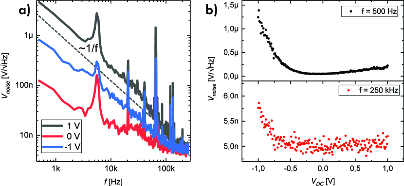
A test device with ground-signal-ground pads and an identical diode to the one in the rectenna has been fabricated to measure the voltage noise directly on-chip. Figure 4a shows the noise at different bias levels at frequencies between 500 Hz and 250 kHz. The bias dependence of the voltage noise is shown in Figure 4b. The noise equivalent power () of the detector can be calculated from the voltage noise and the responsivity . At 250 kHz (500 Hz), the minimum NEP is 81.0 pW/ (3.5 nW/) at a bias voltage of 1 V and 4.3 nW/ (44.1 nW/) at zero bias.
| detector + antenna | [GHz] | [] | NEP [] | diode | flexible | ref. | |
|---|---|---|---|---|---|---|---|
| MIM + bowtie∗ | 28300 | ✓ | 27 | ||||
| traveling wave MIM + bowtie∗ | 28300 | ✓ | 28 | ||||
| GFET + bowtie | 487 | 3000 | ✓ | 26 | |||
| CNT Schottky | 540 | 20000 | 29 | ||||
| photothermoelectric | 2519 | 1100 | 30 | ||||
| MSM + log spiral∗ | 300 | 100 | ✓ | 31 | |||
| flexible 1D-MIG + bowtie | 167 | 81 (3500) | ✓ | ✓ | |||
| unipolar nanodiode + bowtie | 1500 | 330 | ✓ | 32 | |||
| photothermoelectric∗ | 2519 | 16 | 30 | ||||
| ballistic diode + bowtie∗ | 685 | 34 | ✓ | 33 |
* responsivity calculated from incident or absorbed rather than emitted power
Table 1 compares our rectenna on a flexible substrate to other THz detectors from literature.
The rectenna shows a higher responsivity than MIM or metal-semiconductor-metal (MSM) based rectennas, despite being fabricated on a flexible substrate.
It also outperforms the only other reported flexible THz detector by Yang et al. based on a graphene field-effect transistor 26 and most other THz detectors based on the absorption effects.
It should be noted that many references derive values for the optical responsivity from the incident or absorbed power on the device area.
Since our reported optical responsivity uses the total emitted power from the source (not scaled to the device area), it represents a lower bound that is mainly limited by the impedance mismatch between diode and antenna and absorption and scattering in the beam path.
In summary, we have demonstrated detection of THz signals through an edge-contacted graphene-based rectenna in free space measurements.
The flexible rectenna, fabricated using scalable, thin-film compatible processes and CVD-grown graphene, reaches a responsivity of 83.7 V/W at 167 GHz with a NEP of 81.0 pW/, enabling low-cost energy harvesting at the chip level in flexible electronics.
1 Author Information
1.1 ORCID
-
•
Andreas Hemmetter: 0000-0002-0932-2183
-
•
Xinxin Yang: 0000-0003-4464-6922
-
•
Zhenxing Wang: 0000-0002-2103-7692
-
•
Martin Otto: 0000-0001-6704-3468
-
•
Burkay Uzlu: 0000-0001-6776-8901
-
•
Marcel Andree: 0000-0003-3645-0831
-
•
Ullrich Pfeiffer: 0000-0002-6753-7879
-
•
Andrey Vorobiev: 0000-0003-2882-3191
-
•
Jan Stake: 0000-0002-8204-7894
-
•
Daniel Neumaier: 0000-0002-7394-9159
-
•
Max C. Lemme: 0000-0003-4552-2411
1.2 Author contributions
The experiments have been conceived by A.H., Z.W. ,M.L. and D.N. A. H. designed the devices, and performed the electrical characterization. A.H., M.O. and B.U. fabricated the devices. X. Y. performed the electrical and optical characterization. M. A. performed the noise measurement. All authors contributed to discussions and the analysis and interpretation of the results. All authors have given approval to the final version of the manuscript.
1.3 Notes
The authors declare no competing financial interest.
This research was financially supported by the EU projects Graphene Flagship (Contract No. 881603) and WiPLASH (Contract No. 863337) and the DFG projects HiPeDi (Contract No. WA4139/1.1) and GLECS-2 (Contract No. NE1633/3).
References
- Tonouchi 2007 Tonouchi, M. Cutting-edge terahertz technology. Nature Photonics 2007, 1, 97–105
- Siegel 2002 Siegel, P. H. Terahertz technology. IEEE Transactions on Microwave Theory and Techniques 2002, 50, 910–928
- Mittleman 2003 Mittleman, D., Ed. Sensing with Terahertz Radiation; Springer Berlin Heidelberg, 2003
- Sizov and Rogalski 2010 Sizov, F.; Rogalski, A. THz detectors. Progress in Quantum Electronics 2010, 34, 278–347
- Huang et al. 2015 Huang, X.; Leng, T.; Zhu, M.; Zhang, X.; Chen, J.; Chang, K.; Aqeeli, M.; Geim, A. K.; Novoselov, K. S.; Hu, Z. Highly Flexible and Conductive Printed Graphene for Wireless Wearable Communications Applications. Scientific Reports 2015, 5
- Bolívar et al. 2004 Bolívar, P. H.; Nagel, M.; Richter, F.; Brucherseifer, M.; Kurz, H.; Bosserhoff, A.; Büttner, R. Label-Free THz Sensing of Genetic Sequences: Towards ’THz Biochips’. Philosophical Transactions: Mathematical, Physical and Engineering Sciences 2004, 362, 323–335
- Moddel and Grover 2013 Moddel, G., Grover, S., Eds. Rectenna Solar Cells; Springer New York, 2013
- Zhu et al. 2013 Zhu, Z.; Joshi, S.; Grover, S.; Moddel, G. Graphene geometric diodes for terahertz rectennas. Journal of Physics D: Applied Physics 2013, 46, 185101
- Brown et al. 1965 Brown, W.; Mims, J.; Heenan, N. An experimental microwave-powered helicopter. 1958 IRE International Convention Record. 1965; pp 225–235
- Pfeiffer et al. 2008 Pfeiffer, U. R.; Mishra, C.; Rassel, R. M.; Pinkett, S.; Reynolds, S. K. Schottky Barrier Diode Circuits in Silicon for Future Millimeter-Wave and Terahertz Applications. IEEE Transactions on Microwave Theory and Techniques 2008, 56, 364–371
- Sankaran and O 2005 Sankaran, S.; O, K. Schottky barrier diodes for millimeter wave detection in a foundry CMOS process. IEEE Electron Device Letters 2005, 26, 492–494
- Gammon et al. 2012 Gammon, P. M.; Donchev, E.; Pérez-Tomás, A.; Shah, V. A.; Pang, J. S.; Petrov, P. K.; Jennings, M. R.; Fisher, C. A.; Mawby, P. A.; Leadley, D. R.; Alford, N. M. A study of temperature-related non-linearity at the metal-silicon interface. Journal of Applied Physics 2012, 112, 114513
- Georgiadou et al. 2020 Georgiadou, D. G.; Semple, J.; Sagade, A. A.; Forstén, H.; Rantakari, P.; Lin, Y.-H.; Alkhalil, F.; Seitkhan, A.; Loganathan, K.; Faber, H.; Anthopoulos, T. D. 100 GHz zinc oxide Schottky diodes processed from solution on a wafer scale. Nature Electronics 2020, 3, 718–725
- Gadalla et al. 2014 Gadalla, M. N.; Abdel-Rahman, M.; Shamim, A. Design, Optimization and Fabrication of a 28.3 THz Nano-Rectenna for Infrared Detection and Rectification. Scientific Reports 2014, 4
- Shriwastava and Tripathi 2019 Shriwastava, S.; Tripathi, C. C. Metal–Insulator–Metal Diodes: A Potential High Frequency Rectifier for Rectenna Application. Journal of Electronic Materials 2019, 48, 2635–2652
- Periasamy et al. 2011 Periasamy, P.; Berry, J. J.; Dameron, A. A.; Bergeson, J. D.; Ginley, D. S.; O'Hayre, R. P.; Parilla, P. A. Fabrication and Characterization of MIM Diodes Based on Nb/Nb2O5 Via a Rapid Screening Technique. Advanced Materials 2011, 23, 3080–3085
- Urcuyo et al. 2016 Urcuyo, R.; Duong, D. L.; Jeong, H. Y.; Burghard, M.; Kern, K. High Performance Graphene-Oxide-Metal Diode through Bias-Induced Barrier Height Modulation. Advanced Electronic Materials 2016, 2, 1600223
- Shaygan et al. 2017 Shaygan, M.; Wang, Z.; Elsayed, M. S.; Otto, M.; Iannaccone, G.; Ghareeb, A. H.; Fiori, G.; Negra, R.; Neumaier, D. High performance metal–insulator–graphene diodes for radio frequency power detection application. Nanoscale 2017, 9, 11944–11950
- Wang et al. 2019 Wang, Z.; Uzlu, B.; Shaygan, M.; Otto, M.; Ribeiro, M.; Marín, E. G.; Iannaccone, G.; Fiori, G.; Elsayed, M. S.; Negra, R.; Neumaier, D. Flexible One-Dimensional Metal–Insulator–Graphene Diode. ACS Applied Electronic Materials 2019, 1, 945–950
- Cowley and Sorensen 1966 Cowley, A. M.; Sorensen, H. O. Quantitative Comparison of Solid-State Microwave Detectors. IEEE Transactions on Microwave Theory and Techniques 1966, 14, 588–602
- Wang et al. 2013 Wang, L.; Meric, I.; Huang, P. Y.; Gao, Q.; Gao, Y.; Tran, H.; Taniguchi, T.; Watanabe, K.; Campos, L. M.; Muller, D. A.; Guo, J.; Kim, P.; Hone, J.; Shepard, K. L.; Dean, C. R. One-Dimensional Electrical Contact to a Two-Dimensional Material. Science 2013, 342, 614–617
- Ni et al. 2007 Ni, Z. H.; Wang, H. M.; Kasim, J.; Fan, H. M.; Yu, T.; Wu, Y. H.; Feng, Y. P.; Shen, Z. X. Graphene Thickness Determination Using Reflection and Contrast Spectroscopy. Nano Letters 2007, 7, 2758–2763
- de la Rosa et al. 2013 de la Rosa, C. J. L.; Lindvall, N.; Cole, M. T.; Nam, Y.; Löffler, M.; Olsson, E.; Yurgens, A. Frame assisted H2O electrolysis induced H2 bubbling transfer of large area graphene grown by chemical vapor deposition on Cu. Applied Physics Letters 2013, 102, 022101
- Robinson et al. 2011 Robinson, J. A.; LaBella, M.; Zhu, M.; Hollander, M.; Kasarda, R.; Hughes, Z.; Trumbull, K.; Cavalero, R.; Snyder, D. Contacting graphene. Applied Physics Letters 2011, 98, 053103
- Kretz et al. 2018 Kretz, B.; Pedersen, C. S.; Stradi, D.; Brandbyge, M.; Garcia-Lekue, A. Atomistic Insight into the Formation of Metal-Graphene One-Dimensional Contacts. Physical Review Applied 2018, 10
- Yang et al. 2017 Yang, X.; Vorobiev, A.; Generalov, A.; Andersson, M. A.; Stake, J. A flexible graphene terahertz detector. Applied Physics Letters 2017, 111, 021102
- Jayaswal et al. 2018 Jayaswal, G.; Belkadi, A.; Meredov, A.; Pelz, B.; Moddel, G.; Shamim, A. Optical rectification through an Al2O3 based MIM passive rectenna at 28.3 THz. Materials Today Energy 2018, 7, 1–9
- Pelz et al. 2016 Pelz, B.; Belkadi, A.; Moddel, G. Traveling-wave metal-insulator-metal diodes for infrared rectennas. 2016 IEEE 43rd Photovoltaic Specialists Conference (PVSC). 2016
- Manohara et al. 2005 Manohara, H. M.; Wong, E. W.; Schlecht, E.; Hunt, B. D.; Siegel, P. H. Carbon Nanotube Schottky Diodes Using Ti-Schottky and Pt-Ohmic Contacts for High Frequency Applications. Nano Letters 2005, 5, 1469–1474
- Cai et al. 2014 Cai, X.; Sushkov, A. B.; Suess, R. J.; Jadidi, M. M.; Jenkins, G. S.; Nyakiti, L. O.; Myers-Ward, R. L.; Li, S.; Yan, J.; Gaskill, D. K.; Murphy, T. E.; Drew, H. D.; Fuhrer, M. S. Sensitive room-temperature terahertz detection via the photothermoelectric effect in graphene. Nature Nanotechnology 2014, 9, 814–819
- Moon et al. 2018 Moon, K.; Shin, J.-H.; Lee, I.-M.; Park, D. W.; Lee, E. S.; Park, K. H. Terahertz rectifier exploiting electric field-induced hot-carrier effect in asymmetric nano-electrode. Nanotechnology 2018, 29, 47LT01
- Balocco et al. 2011 Balocco, C.; Kasjoo, S. R.; Lu, X. F.; Zhang, L. Q.; Alimi, Y.; Winnerl, S.; Song, A. M. Room-temperature operation of a unipolar nanodiode at terahertz frequencies. Applied Physics Letters 2011, 98, 223501
- Auton et al. 2017 Auton, G.; But, D. B.; Zhang, J.; Hill, E.; Coquillat, D.; Consejo, C.; Nouvel, P.; Knap, W.; Varani, L.; Teppe, F.; Torres, J.; Song, A. Terahertz Detection and Imaging Using Graphene Ballistic Rectifiers. Nano Letters 2017, 17, 7015–7020