[1]Lukas Windgätter
[1]Simone Latini
[1,5,8]Angel Rubio
1]Max Planck Institute for the Structure and Dynamics of Matter, Luruper Chaussee 149, 22761 Hamburg, Germany
2] Radboud University, Institute for Molecules and Materials, Heijendaalseweg 135, 6525 AJ Nijmegen, Netherlands
3]Collège de France, 11 place Marcelin Berthelot, 75005 Paris, France
4] Center for Computational Quantum Physics, Flatiron Institute, New York, New York 10010, USA
5] CPHT, CNRS, Ecole Polytechnique, IP Paris, F-91128 Palaiseau, France
6]Department of Quantum Matter Physics, University of Geneva, Quai Ernest-Ansermet 24, 1211 Geneva, Switzerland
7]Department of Physics, Columbia University, New York, New York 10027, USA
8]Nano-Bio Spectroscopy Group, Departamento de Física de Materiales, Universidad del País Vasco, 20018 San Sebastian, Spain
Common microscopic origin of the phase transitions in Ta2NiS5 and the excitonic insulator candidate Ta2NiSe5
Abstract
The structural phase transition in Ta2NiSe5 has been envisioned as driven by the formation of an excitonic insulating phase. However, the role of structural and electronic instabilities on crystal symmetry breaking has yet to be disentangled. Meanwhile, the phase transition in its complementary material Ta2NiS5 does not show any experimental hints of an excitonic insulating phase. We present a microscopic investigation of the electronic and phononic effects involved in the structural phase transition in Ta2NiSe5 and Ta2NiS5 using extensive first-principles calculations. In both materials the crystal symmetries are broken by phonon instabilities, which in turn lead to changes in the electronic bandstructure also observed in experiment. A total energy landscape analysis shows no tendency towards a purely electronic instability and we find that a sizeable lattice distortion is needed to open a bandgap. We conclude that an excitonic instability is not needed to explain the phase transition in both Ta2NiSe5 and Ta2NiS5.
1 Introduction
The excitonic insulator phase has been theoretically proposed in the 1960s Kohn1967 ; Jerome1967 ; Mott1961 ; Keldysh1968 ; Halperin1968 ; Kozlov1965 and is predicted to appear in semiconductors (or semimetals) with excitonic binding energies larger than the bandgap (or bandoverlap) of their conventional groundstate. Under this condition, the groundstate becomes unstable against the spontaneous formation of bound electron hole pairs, i.e. excitons. Depending on the conventional phase being semiconducting or semimetallic, the transition is described by a Bose-Einstein condensation (BEC) or a Bardeen-Cooper-Schrieffer (BCS) like mechanism respectively Keldysh1968 ; Jerome1967 ; Halperin1968 .
A major challenge in the experimental detection of an excitonic insulator state in a crystal is that the excitonic transition is coupled to other degrees of freedom, such as lattice distortions, which make an unambiguous detection difficult.
This is the reason why several materials such as 1T-TiSe2 Cercellier2007 ; Kogar2017 or TmSe0.45Te0.55 TmSeTe1 have not been unambiguously confirmed to host an excitonic insulating (EI) groundstate. These are indirect bandgap or semi-metal materials which exhibit finite momentum ordering and in the case of 1T-TiSe2, for example, the existence of a charge density wave masks the possible presence of an excitonic insulating phase.
Very recently also two-dimensional materials have shown promises to host an excitonic groundstate. Experimentally, strong evidence for the existence of excitonic insulating phases have been provided both for transition metal dichalcogenides (TMD) bilayers KinFaiMak and monolayers such as WTe2 and MoS2 MonolayerWTe2 ; Varsano2020 . An extensive theoretical study has identified several candidate material combinations for hetero-bilayers that could host an excitonic insulator by analyzing the electronic properties of a wide range of materials MaterialSearch .
Further low dimensional excitonic insulator candidates are carbon nanotubes Varsano2017 , Sb nanoflakes Li2019 , double bilayer graphene Li2017_2 ; Perali2013 and topological systems Hu2018 such as InAs/GaSb Du2017 .
In the bulk phase, MoS2 has recently revealed as another candidate material since its bandgap can be tuned via pressure, yielding excitonic binding energies larger than the quasi-particle gap, which would allow for a transition into a possibly excitonic insulating groundstate MoS2Pressure .
We investigate bulk Ta2NiSe5 (TNSe), which is considered to be a very promising candidate to host an excitonic condensate Kaneko2013 , with several experimental evidence suggesting an EI groundstate: Angle resolved photo electron spectroscopy (ARPES) measurements have shown a characteristic band flattening near the -point upon cooling below the critical temperature Wakisaka2009 ; Seki2014 ; Watson2020 ; tang2020 , a dome-shaped bandgap-temperature phase diagram, similar to the theoretically predicted one, has been found Lu2017 and the opening of a gap has been measured in scanning tunnel spectroscopy (STS)Lee2019 , optics Lu2017 and ARPES Baldini2020 ; Watson2020 experiments below the critical temperature Lee2019 . The bandgap in the low-temperature phase is reported to be between 160 meV in opticsLu2017 and 300 meV in STS measurements Lee2019 .
The current literature is controversially reporting the high temperature phase of TNSe to be either a direct bandgap semi-conductor Kaneko2012 ; Kaneko2013 or a small bandoverlap semi-metalWatson2020 . It is however agreed that there exists a structural phase transition, and possibly a transition into an excitonic groundstate, at the critical temperature Tc=326K Lu2017 ; Nakano2018 ; DiSalvo1986 ; Sunshine1985 . The structural transition has been reported to be from a high-temperature orthorhombic to a low-temperature monoclinic phase Nakano2018 ; DiSalvo1986 ; Sunshine1985 .
On the other hand Ta2NiS5 (TNS), a material of the same structure of TNSe with Sulfur replacing Selenium, does not exhibit the same excitonic signatures of TNSe, such as band flattening and bandgap opening. Indeed a structural transition at 120K Blumberg2021 has been reported without the formation of flat bands or a metal to semiconductor transition Mu2018 .
Due to the uncertainty on whether TNSe has a semi-metallic or gapped high-temperature phase, from a theoretical perspective it is unclear which mechanism between BEC and BCS can be applied. In fact experimentally there is no unambiguous evidence that excitons are involved in the phase transition at all. These facts indicate that, in relation to TNSe, the concept of excitonic insulator can be source of confusion, as it has been generally employed to refer to a phase showing a characteristic gap opening and band flattening Wakisaka2009 ; Seki2014 ; tang2020 ; Lee2019 without direct observation of excitonic features and/or excitonic condensation.
A recent symmetry analysis of the possible electronic instabilities issuing from the electron-electron interactions has shown that the electronic phase transitions in the material should not be be ascribed to a condensation phenomenon but rather to the electronic lowering of the discrete lattice symmetry Mazza2020 , which corresponds to the breaking of a continuous U(1) symmetry during the excitonic phase transition. This observation, together with other recent experimental and theoretical observations Watson2020 ; subedi2020 , suggest a prominent role of structural instabilities in the system. In this work, we abandon the concept of excitonic condensation and show that the experimental features of TNSe and TNS mentioned above can be completely explained without explicitly taking the formation of excitons into account. We demonstrate how the electronic and structural properties of the two crystals can be rationalised in terms of electronic and intrinsic lattice instabilities that drive the system from the orthorhombic to monoclinic phase. The occurrence of such a lattice driven instability agrees with a prior report of Alaska Subedi subedi2020 .
We present a comprehensive ab-initio study using Density Functional Theory (DFT) for the transition from the orthorhombic to the monoclinic phase beyond standard generalized gradient approximation (GGA) functionals. In section 2.1 we start by investigating the structural stability of the system and show, that at low temperature a monoclinic groundstate is energetically favoured to the orthorhombic one, which suggests the existence of a lattice instability. A similar analysis applied to TNS highlights an equivalent structural transition mechanism from an orthorhombic to a C2/c symmetric monoclinic cell.
In section 2.2 we then investigate the electronic bandstructure of both the high and low-temperature phase of TNSe and TNS using different exchange correlation functionals with increasing accuracy. For TNSe, we can establish the orthorhombic groundstate to be metallic and observe a sizeable gap opening as well as a band flattening with the phase transition. This shows that for this material the structural distortion is essential for the bandgap opening observed in optics and STS measurements and cannot be explained considering only the electronic degrees of freedom. In section 2.3 we show, that a similar finding results from our many body perturbation theory based calculations carried out at the G0W0 level. Performing an equivalent DFT analysis for TNS shows that both the orthorhombic and monoclinic phases are gapped systems with parabolic electronic dispersions at . This explains why a metal to semiconductor transition and band flattening, which have been characterised as a signature of an excitonic insulator in TNSe, has not been observed for TNS Mu2018 .
We then show, that electronic heating enhances the valence band flattening and investigate in the following section 2.5 the origin of the instability observed in TNSe. We find no evidence for an electronically-driven spontaneous symmetry breaking in the TNSe charge density upon infinitesimal lattice distortions. In the symmetry broken lattice structure the total energy is, however, clearly lowered, which renders the electron-phonon interaction the main driving mechanism for the structural transition. In section 2.6 we discuss the phononic bandstructure and single out the phononic instabilities of the orthorhombic phase, the ones that could possibly drive the structural transition. A detailed discussion of the obtained phonon modes in relation with the most recent Raman measurements shows that we are able to reproduce all phonon peaks, except for the first two B modes, which exhibit a strong broadening, which hints to a strong coupling of these modes to other degrees of freedom. Finally in section 2.7 we show that the electronic dispersion is strongly modulated by different phonon modes. In particular it is expected that thermal occupation of the phonon mode responsible for the structural transition leads to a further bandgap opening
2 Results
2.1 Structure Relaxation
TNSe is a layered material bound by van-der Waals forces. It consists of parallel Tantalum and Nickel chains and is thus referred to as a quasi 1D-material (see Fig. 1) Sunshine1985 . Experimentally the high-temperature phase exhibits an orthorhombic structure which is distorted to a monoclinic structure in the low-temperature phase. The distortion, however, is subtle with a change in the angle (see Fig. 2b) of just 0.53∘ Sunshine1985 to 0.69∘ Nakano2018 .
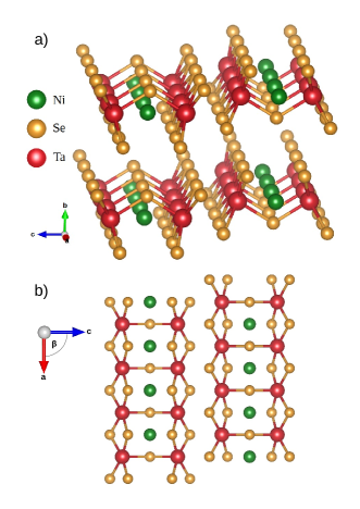
We have performed a first-principles structure relaxation of atomic coordinates, cell shape and cell volume for different functionals. In all cases the relaxation resulted in a triclinic structure. The resulting lattice parameters are shown in the Supplementary Tables 1 and 5: the two functionals vdW-optB88 and vdW-optPBE Klime2011 ; Klimes2010 , which include van-der Waals corrections, result in relaxed structures which agree well with the experimentally measured values, while the PBE functionals overestimates the experimentally measured interlayer lattice parameter b by 10.5% Nakano2018 (see Supplementary Table 1 and 5). As expected this shows the importance of including van-der Waals forces when describing layered structures such as TNSe.
The angles of the relaxed triclinic structure are , and . As the two angles and are almost rectangular, the triclinic cell and the corresponding monoclinic cell are almost degenerate. Furthermore, we have checked that the small triclinic distortion does not modify the electronic properties compared to the exact monoclinic structure. Thus in the following, we refer to the fully relaxed structure as monoclinic . The monoclinic angle agrees well with the experimentally measured values Nakano2018 and Sunshine1985 .
To obtain the relaxed geometry for the high-temperature orthorhombic cell, we have performed the same relaxation using the vdw-optB88 functional enforcing the orthorhombic symmetry. The resulting lattice parameters are shown in the Supplementary Tables 2 and 4. As the relaxed structure predicted by the vdW-optB88 functional has the best agreement with the experimentally measured values for both the monoclinic and orthorhombic phase, we have chosen it for all following structural calculations.
We have performed similar relaxations for the Sulfur compound: A full relaxation using the vdW-optB88 functional, again, results in a triclinic geometry that is almost degenerate with the monoclinic cell. The monoclinic angle is . For the orthorhombic phase we have performed a further relaxation with fixed symmetry. The lattice parameters for both structures are shown in Supplementary Table 3 and agree very well with the experimentally measured values from X-ray diffraction. This agrees with a recent Raman study by M.Ye et al which reports an orthorhombic high temperature phase and a structural transition to a monoclinic phase at T=120K Blumberg2021 .
Therefore we find, that in both TNSe and TNS a monoclinic geometry is energetically favoured, which shows that a similar lattice instability occurs in both materials. In section 2.6 we extensively discuss the phononic properties of the two materials and identify the structural instability with an unstable B phonon. Although the structural change between monoclinic and orthorhombic phase is small, the modifications for the electronic bandstructure with the phase transition is significant (see section 2.2). This hints to a strong coupling between electronic and lattice degrees of freedom (see section 2.7).
2.2 Electronic Bandstructure
In this section we present a complete and systematic DFT study of both TNSe and TNS using standard and more accurate functionals. While we find that the fine electronic properties are sensitive to the details of exchange and correlation, the underlying mechanism of bandgap opening due to the structural phase transition is independent of the functional choice for both TNSe and TNS.
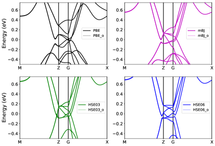
We investigate the bandstructure of the orthorhombic and monoclinic geometries using different exchange correlation functionals which include varying degrees of exact exchange. These are ranked in chemical accuracy with the PBE functional Perdew1996 being the most inaccurate, but computationally least demanding, followed by the modified Becke-Johnson (mBJ) functional Tran2009 ; Becke2006 ; Becke1989 and finally the range separated hybrid functional HSE03 Heyd2003 being the most accurate one.
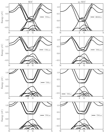
The results are shown in Fig. 2. Results for the HSE06 functional are reported Supplementary Figure 9 and the definition of the M-Z--X path is given in Supplementary Note 1.
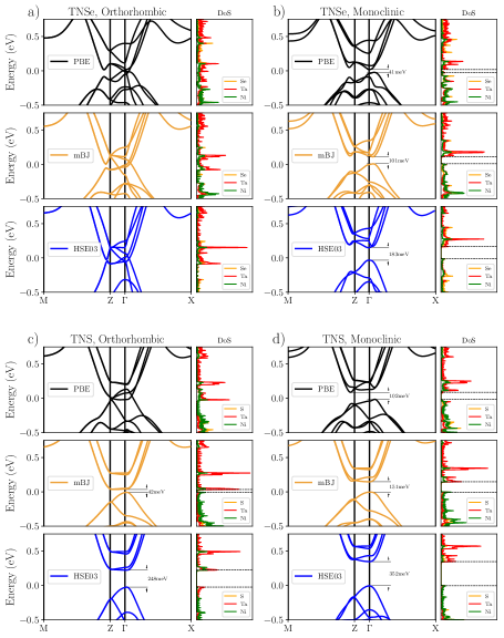
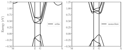
Panels (a) and (b) of Fig. 2 display the obtained bandstructure of TNSe: the high temperature orthorhombic structure exhibits a metallic groundstate independently of the functional presented here, while the monoclinic structure is always semi-conducting. The bandgap opening is sizeable for all investigated functionals and its position and value changes with the amount of exchange and correlation included. With the PBE functional we obtain an indirect bandgap value of 40 meV, with the modified Becke-Johnson (mBJ) functional a direct bandgap of 101 meV and with the HSE03 functional a direct bandgap of 183 meV. Thus, the bandgap grows with an increasing accuracy of the exchange and correlation functional. From Fig. 2b) we observe that in the monoclinic phase, TNSe has a rather flat dispersion around due to the valence band maxima being off for both the PBE and mBJ functional.
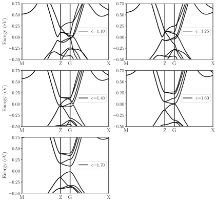
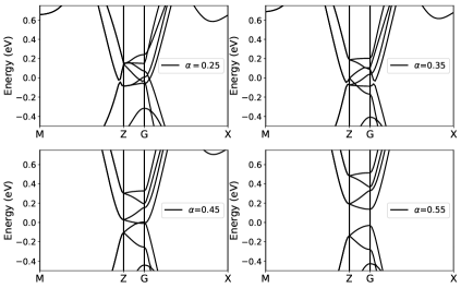
By increasing the exchange contribution included in the functional, e.g. by tuning the mixing parameter in the hybrid functional or the c parameter in the mBJ-functional, it is possible to further increase the bandgap. We observed that even in the orthorhombic phase increasing the exchange contribution can lead to a gap opening (see Supplementary Note 4 and Supplementary Figures 5 and 6) which is consistent with prior studies Sugimoto2018 . The bandgap opening resulting from HSE03 agrees well with the experimentally measured bandgap of 160 meV Lu2017 . In STS measurements a gap of 300 meV has been reported Lee2019 . However, we notice that the structure in Ref.Lee2019 shows a monoclinic distortion with an angle 92.5∘,i.e. much larger than the angle reported in previous studies and the angle obtained in our calculation (). Correcting for this difference we find that both the optics and STM results are in good agreement with our HSE03 results (see Supplementary Note 6 for more details).
Performing similar calculations for TNS, Fig. 2(c) and (d), we identify a major difference in the electronic behaviour of the Selenium and Sulfur compounds. We see that using either mBJ or HSE03 hybrid functionals, the calculations predict a semiconducting groundstate even for the orthorhombic geometry. The structural transition to the monoclinic cell then leads to a further bandgap opening, with bandgap values being around twice the size of the TNSe ones. Therefore, in contrast to TNSe, no metal to insulator transition is observed. The bandgap is direct at the -point with a parabolic dispersion towards the X direction. These findings agree well with the theoretical and experimental reports: ARPES as well as optical conductivity data show that TNS has a parabolic dispersion around the -point Mu2018 ; Sugimoto2018 with a robust bandgap of 200 meV Mu2018 ; Li2017 ; Sugimoto2018 and 250 meV in optics Larkin2017 .
We stress that while both compounds have a similar lattice instability from orthorhombic to monoclinic geometry, in the case of TNSe the structural instability is accompanied by a metal-to-insulator transition which is absent in the case of TNS.
These observations match all known experimental trends for these two systems.
In the case of the Selenium compound the metal-insulator transition accompanied by the flattening of the valence band around appears to be the intrinsic outcome of the structural instability of the system and not the distinctive signature of the excitonic insulator phase, as it has been interpreted so far. We support this statement in the next sections by explicitly accounting for the role of the electronic instability and comparing the excitonic binding energy with the bandgap value.
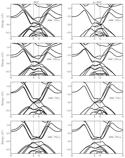
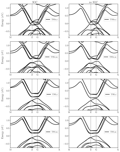
Given that states near the band gap have significant contributions from Ta, we have checked the validity of our results by also including spin-orbit coupling (SOC) effects and reported the related band structure calculations in the Supplementary Figures 2-4, Supplementary Note 3 and Supplementary Table 6. We find that besides a band splitting in the M-Z direction and a minor renormalization of the bandgap, all our claims remain unchanged.
2.3 G0W0 calculations
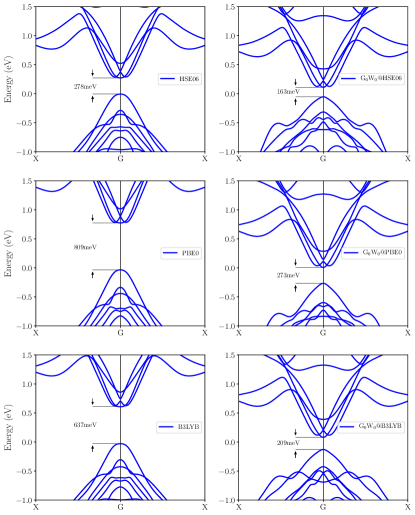
While DFT calculations generally provide a good starting point for discussing material properties they often lack quantitative agreement with experimental results. It is known that one needs to add many body corrections to obtain a quantitative agreement with the experimental bandgaps. The standard approach which provides accurate bandgaps is the GW method Schilfgaarde2006 ; Onida2002 ; Hybertsen1985 ; Hybertsen1986 . The latter is a many-body theory approach which consists in solving Hedin’s equations iteratively Hedin1965 while neglecting vertex corrections. There exist various flavours of the GW approximation with the G0W0 being the most commonly used. In G0W0 one approximates the starting wavefunctions to be the DFT ones and performs only one cycle of Hedin’s equation to compute the self energy and correct the electronic states energies. As such the G0W0 approximation relies on the DFT wavefunctions to provide a good description of the full many body wavefunction and it is crucial to investigate the starting point dependence of the G0W0 approximation. We have performed calculations using the wavefunctions and electronic dispersion resulting from PBE and HSE03 functional calculations (more hybrid functional starting points are shown Supplementary Figure 10). The corresponding bandstructures for the monoclinic geometry of TNSe can be seen in Fig. 3.
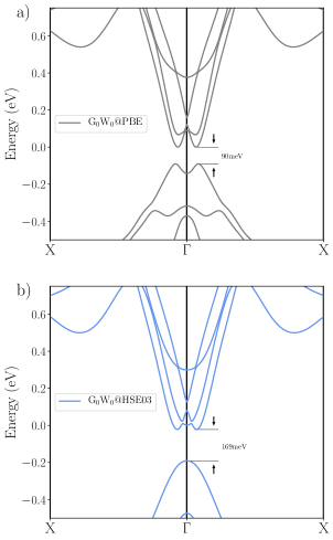
Independently of the starting point, the bandgap converges towards a similar value, increasing in the PBE case, where it is commonly underestimated, and decreasing for the HSE03 functional. In all cases G0W0 predicts a bandgap between 100 meV and 163 meV which is in good agreement with the experimental gap of 160 meV measured in optics Lu2017 . The dispersion of the conduction bands shows similar features with a pronounced double well shape in X--X direction. The valence band dispersion, however, differs between the PBE and the HSE, with the PBE one being M-shaped and the HSE one being parabolic. This is inherited from the different initial DFT wavefunctions and electronic dispersion.
The comparison of the electronic dispersion with recent ARPES measurements by Baldini et al.Baldini2020 shows that the dispersion obtained using the PBE functional as starting point agrees well with the experimentally measured one, reproducing both the flat valence band as well as the Mexican hat shaped conduction band. Also Tang et al. tang2020 and Watson et al. Watson2020 report an M-shaped valence band which agrees well with the G0W0@PBE calculation. This reinforces the conclusion that the band structure in the monoclinic phase correctly
accounts for the metal-to-insulator transition. A detailed quantitative comparison to experimental
results, however, can only be achieved by including correlation beyond the PBE functional.
We also solved the Bethe-Salpether equation (BSE) starting from the G0W0 results Salpeter1951 ; Sander2015 to explicitly account for exciton formation. While full convergence is not feasible with our computational resources, we can extrapolate from our k-point dependent results BSE results on top of G0W0 and verify that the excitonic binding energy is smaller than the G0W0 gap in the monoclinic phase (see Supplementary Notes 7 and 8 and Supplementary Figures 13-19). This is an indication that the condition needed for an excitonic insulating phase, i.e. an exciton binding energy larger than the gap, is not fulfilled in TNSe for the monoclinic phase.
2.4 The effect of electronic Heating
The interpretation of an excitonic insulator as a phase consisting of an excitonic condensate entails that an increase of temperature above a critical value leads to the melting of the condensate and hence to a bandgap closing. Experiments aimed at demonstrating such a behaviour to prove the possibility of excitonic condensation in TNSe, have indeed reported bandgap opening and band flattening for increasing pump fluence tang2020 . Here we mimic the photoexcitation with a thermal distribution of electrons and holes and show that the variation of the bandgap and the band flattening can be explained via a temperature increase in the same manner as in standard semiconductors. Indeed, an increase of temperature of the thermal distribution generates free carriers and it has been shown that for low carrier densities the bandgap shrinks and eventually increases again for sufficiently high densities Sparatu2004 ; Beni1978 . The mechanism behind such a bandgap variation can be rationalized in terms of effective screening of the Coulomb interaction which modulates the effect of bandgap opening caused by the exchange contribution.
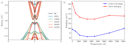
To approximately investigate the enhanced screening effects due to free carriers, we have performed a set of G0W0 calculations for different electronic temperatures. The electronic temperatures have been set by changing the temperature in the Fermi-Dirac function used for the occupation smearing of the Kohn-Sham states in the self-consistent DFT calculations. This effectively leads to a depletion of electrons in the valence bands and a finite electronic occupancy of the conduction bands. Specifically we have investigated Fermi-Dirac distributions with temperatures ranging between K and K. G0W0 calculations on such thermalized groundstates can then provide bandstructures which include the effect of the screening due to the thermally excited carriers. The resulting bandstructures and bandgap renormalizations are presented in Fig. 4(a) and Fig. 4(b). One observes that introducing charged carriers to the conduction bands rapidly decreases the bandgap. It reaches its minimum around 2500K with a bandgap smaller than its equilibrium value and reopens for higher temperatures. This behaviour is consistent with the typical bandgap renormalization in standard semiconductors mentioned above. The pronounced double well feature of the valence band slightly flattens out as the -point energy is shifted upwards (see Fig. 4(a)) and only for electronic temperature higher than K the bandstructure changes significantly, which explains the upwards trend in the bandgap for high temperatures. To reach such high electronic temperatures with a laser, however, is experimentally unrealistic as it would damage the material.
We remark that, even though the applied computational procedure does not properly describe the experimental photoexcitation of electrons into conduction bands, we could expect a behaviour similar to the one described above upon intensive laser pumping.
2.5 Origin of the Structural Instability
Having established the importance of the structural instability in the determination of the insulating ground state of TNSe, in this section we discuss possible origins of the structural instability. On general grounds, the structural instability is the result of the complex interplay between the electronic and the lattice degrees of freedom. The possibility of a purely electronic origin of the structural instability, namely a charge density that spontaneously breaks the orthorhombic symmetry at fixed ions position, has been recently discussed in the literature. Specifically, this possibility has been introduced at the model level in Ref. Mazza2020 as the result of an electronic interaction-driven spontaneous hybridization between localized Wannier orbitals of different symmetry. Moreover, experimental data from symmetry-resolved Raman have been interpreted as signatures of quasi-critical charge fluctuations that are active in the corresponding symmetry channel Kim2020 .
We start by recalling the mechanism behind such an electronic instability. The mechanism can be readily understood in terms of the energetic competition between on-site (Ta-Ta and Ni-Ni) and the nearest neighbouring (Ta-Ni) density-density interaction that can render the ground state of the system to be either metallic or insulating. In a simplified description this energetic competition can be well understood as a problem of two electrons in two sites with on-site interaction and inter-site interaction . If the energy of the lowest lying orbitals in the two sites are comparable, the ground state configuration of the problem is entirely determined by the ratio between and . In the limit the lowest energy configuration corresponds to the single occupation of the lowest lying orbitals on the two sites, whereas in the opposite limit the most favourable configuration is the doubly occupation of the site with the lowest energy orbital. The two configurations become quasi-degenerate for such that a coherent superposition between the two configuration due to an exchange interaction mediated by is possible.
Assuming that in the extended system the lowest lying orbitals in the two sites contribute to the formation of two bands close to the Fermi level, the two configurations correspond respectively
to a metal in which both bands are partially occupied or to an insulator in which the lowest lying band is fully occupied. The coherent superposition, instead, indicates the possibility of a spontaneous hybridization between the bands which leads to the opening of an hybridization gap.
As discussed in Ref. Mazza2020 this can happen only if the bands have different symmetry character and therefore an hybridization of this type would correspond to a charge density that breaks the orthorhombic lattice symmetry.
Calculations based on a mean-field ansatz for a realistic model of TNSe show that the spontaneous hybridization transition can occur in a very narrow region around (see inset of Fig. 5), where the factor comes from the fact that there are four neighbouring Ta-atoms around each Nickel. We emphasize that the phase diagram in the inset of Fig. 5) from Ref. Mazza2020 is intended to be qualitative as it is specifically calculated for a set of realistic parameters corresponding to the mBJ functional and a selection of Wannier orbitals, hence not necessarily representative for other functionals.
The smallness of this region suggests that the electronic instability relies on a delicate energetic balance between the competing metallic and insulating states which is not guaranteed to be exactly satisfied in the real material.
We therefore exploit the present full ab-initio results to test this energetic balance in the case of TNSe and, in particular, how it is affected by the lattice distortions which are neglected in the electronic instability discussion above.
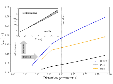
We do so by performing bandgap calculations, reported in Fig. 5, for different functionals on increasingly distorted structures using the distortion parameter . To define the distortion parameter we linearly interpolate between the high symmetric orthorhombic and low symmetric monoclinic geometry:
we parameterized this transition with a transition vector defined as the difference between the atomic configuration of the high symmetry and low symmetry structure , with describing the atomic configuration of the monoclinic cell and describing the atomic configuration of the orthorhombic cell.
Using this vector we can linearly interpolate between the orthorhombic and monoclinic structure via , where is the distortion parameter. The lattice vectors are parameterized in a similar way. This means, that also each of the three lattice vectors of both geometries are linearly interpolated using the difference between the monoclinic and orthorhombic lattice vectors
. Hence, the interpolated lattice vectors are for each of the three lattice vectors.
If a gap opens as a result of the electronic instability only, we could expect that an infinitesimal distortion would be sufficient to stabilize an insulating ground state with a distorted charge density.
However, we observe that, independently of the functional used, a finite critical value of the distortion parameter is needed in order to open a gap (see Fig. 5).
This means that TNSe is indeed likely outside the region where a purely electronic instability can be expected and that a finite distortion of the lattice is critical to account for the metal-insulator transition.
Nonetheless, we observe a cooperation between electronic correlations and lattice distortion in the opening of the gap.
Indeed, by increasing the accuracy of the functional (from PBE to HSE), which corresponds to increasing amount of electronic exchange and correlation,
the bandgap at fixed distortion is increased and the critical value of the distortion parameter needed for opening a gap is significantly reduced.
We therefore conclude that in relation to the simple mean-field phase diagram with tunable and interaction derived for the orthorhombic phase of TNSe, the material must be placed on the semi-metallic region of the phase diagram and that the lattice distortions act in the same direction of the nearest neighbour interaction . On the other hand, based on the previous electronic band structure results, the Sulfur compound must be placed on the semiconducting side of the phase diagram, corresponding to a larger effect of the interaction .
As a further confirmation of the fact that the non-local interaction is responsible for the opening of the gap in these materials we also performed fully ab-initio Hartree-Fock calculations for TNSe which are supposed to include a larger contribution from non-local correlations: both the orthorhombic and the monoclinic phase have semiconducting groundstates with bandgaps of meV and meV respectively (see Supplementary Figure 11).
We finally mention that despite the fact that a purely electronic contribution is absent for TNSe we cannot exclude the system to be close enough to an electronic instability so that quasi-critical charge fluctuations can be present in the symmetry channel corresponding to the breaking of the mirror symmetries that characterizes the transition from the orthorhombic to the monoclinic phase Kim2020 .
This analysis goes beyond the scope of the present work and will be the subject of future investigations.
In the following we focus on the possibility of having an energetically favorable electronic instability which however does not open a bandgap, but instead stays in the metallic regime close to the orthorhombic geometry. We introduce the total energy , as a function of two coordinates. The first one, which accounts for the lattice degrees of freedom, is the lattice distortion . The second coordinate of the energy functional is the component of the electronic charge density which corresponds to a symmetry lowering from orthorhombic to monoclinic (of Mazza2020 ). It is defined as
| (1) |
with R being the orthorhombic symmetry operators and the charge density. For the orthorhombic cmcm geometry of TNSe four different mirror symmetries have been identified as relevant to the orthorhombic to monoclinic transition Mazza2020 , where and and denote mirror symmetries parallel and orthogonal to the chain direction and and denote the corresponding one dimensional chains in the unit cell. We will focus on these mirror symmetries in the following. In this picture the groundstate is defined such that at and the total energy is minimal:
| (2) |
If the system undergoes a spontaneous electronic instability, the charge density breaks the orthorhombic lattice symmetry for infinitesimal distortions and hence:
| (3) |
The two possible scenarios for a lattice and an electronically driven transition are shown schematically in Fig. 6. Panel a) shows the case of a lattice driven phase transition. The charge density component does not break the orthorhombic symmetries at 0 and evolves smoothly towards the groundstate of the system with increasing distortion. Panel b) shows the case of an electronically driven phase transition where the charge density breaks the orthorhombic lattice symmetries. In this case the charge density component does not vanish at 0 but it is finite instead and its value increases with increasing distortion . In both cases a) and b) a finite d-distortion may still be needed to obtain a positive bandgap.
When we perform ab-initio calculations imposing the orthorhombic symmetries, the charge density is automatically symmetrized so that is true by construction. However, if we compute for small lattice distortions that break the orthorhombic symmetry, we can evaluate the limit and verify whether an electronic instability is present. Furthermore, an electronic symmetry breaking should also result in a discontinuity in the total energy for infinitesimal lattice distortion, as a phase with a finite has to lower the energy with respect to the symmetric orthorhombic phase in the electronic instability scenario. Both the computed total energy as well as for fixed lattice distortions are depicted in panels c) and d) of Fig. 6.
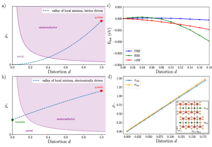
Panel (c) shows, that there is no discontinuity in the total energy. For the vdw-optB88 functional the total energy decreases monotonously to its minimum for increasing (see Supplementary Note 2 and Supplementary Figure 1 for ). For the PBE and HSE functionals it increases first and subsequently decreases towards its minimum, which for the HSE03 functional is at around . We attribute such a non-monotonous behavior to the fact that the distortion parameter is defined with respect to the vdw-optB88 functional structures. This means that in the phase-space of the normal phononic mode we are not moving along the soft phonon modes but along a direction where the orthorhombic phase is a saddle point. Solving this issue would require a structure relaxation using hybrid functionals to obtain the exact soft mode coordinate, which is computationally not feasible for TNSe. Panel (d) shows the evolution of the charge density component for different symmetry operations defined in Ref. Mazza2020 . describes the reflection symmetry parallel the Nickel chain in the xz-plane and describes the reflection in the yz-plane orthogonal to the chain direction and along the Tantalum atoms (see inset Fig. 6). For both reflection symmetries approaches 0 for . This reinforces the conclusion that the transition in TNSe requires a finite lattice distortion and we do not observe a spontaneous electronic instability.
2.6 Phonon Dispersion
So far we have investigated the electronic degrees of freedom focusing on the effect of the lattice geometries. While we have introduced the concept of a structural instability in the prior sections we show how it is related to the lattice dynamics of the crystal.
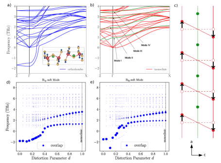
The phonon dispersion of the orthorhombic as well as the monoclinic cell of TNSe are shown in Fig. 7a: the orthorhombic cell shows two unstable optical phonon modes around the -point, characterized by imaginary frequencies (indicated as negative values here), while the monoclinic cell shows no phonon instabilities.
The two unstable phonon modes belong to the B and B symmetry groups. Both unstable phonons lead to monoclinic distortions and become stable in the monoclinic phase. The B leads to a P21/m geometry and the B mode leads to the C2/c symmetry. Just displacing the atoms within the unit cell and computing the total energy of the structure shows that the P21/m would be favored subedi2020 , however, also allowing for lattice distortions the C2/c symmetry is favored with an energy difference of 14.4 meV per unit cell. This is in agreement with the full relaxation as well as experimental findings observing a monoclinic C2/c symmetric geometry in the low-temperature phase of TNSe Sunshine1985 ; Nakano2018_2 . Therefore, we can identify the B mode as the relevant structural instability which drives the phase transition. The eigenvector of this mode is displayed in the inset of Fig. 7a. It shows the characteristic monoclinic displacement along the chain direction which results in a shearing of the Ta atoms around the Nickel atom (see Fig. 7c) which has been identified as the order parameter for the orthorhombic to monoclinic phase transition by Kaneko et al. Kaneko2013 . Note, that a similar phonon analysis using ab-initio methods has been performed in Ref.subedi2020 and our calculations agree with this study.
For the sake of comparison we have performed a calculation of the phononic spectrum at the -point for both geometries of TNS. We find one phononic instability in the orthorhombic structure which becomes stable in the monoclinic phase (see Supplementary Table 7). The instability has B symmetry and drives, similarly to the TNSe case, the orthorhombic to monoclinic phase transition, which is consistent with the monoclinic groundstate being the energetically favoured one.
To investigate the evolution of the phonon instabilities when transforming the crystal from orthorhombic to monoclinic, we have performed calculations on increasingly distorted structures using the distortion parameter introduced in the previous section. Performing phonon calculations we obtained the phonon spectra and eigenvectors at the -point for each of the distorted geometries. To follow the evolution of the phonon energies during the structural transition, we have computed the overlap between the orthorhombic eigenvectors of the two phonon instabilities with the phononic eigenvectors of all modes at a given value of the distortion parameter . The result is displayed in Fig. 7c) and d) where the marker size is proportional to such overlaps. Note, that the phonon eigenvectors for a given distortion form an orthonormal system. Therefore, no overlap is visible at 0 for the two unstable modes. As the structure is transformed to the monoclinic cell the different phonons start hybridizing which leads to non-zero overlap of the unstable orthorhombic phonons and the phonons at d0. We observe that the two unstable phonons are being stabilized along the phase transition and hybridize predominantly into a pair of monoclinic phonons. The unstable B has the strongest overlap with the monoclinic 3.4 THz and 1.9 THz phonon modes and the unstable B has the strongest overlap with the monoclinic 3.6 THz and 1.4 THz modes. In section 2.7 we will show, that the two monoclinic B2g phonons couple strongly to the electronic degrees of freedom.
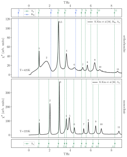
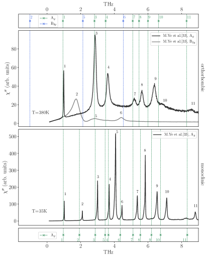
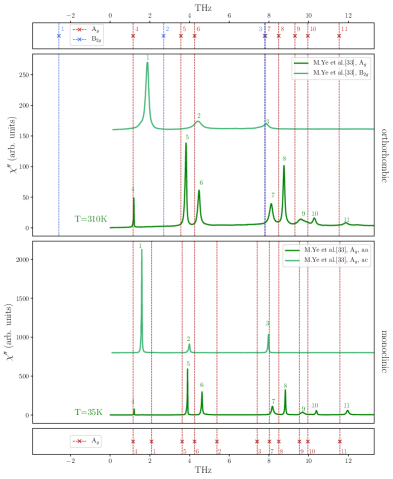
Further analysis of the phonon symmetries allows us to identify all three B and eight A phonon modes of the orthorhombic and all A phonon modes of the monoclinic geometry. Their comparison with the phononic peak positions from recent experimental Raman measurements which are sensitive to B and A symmetry channel Kim2020 ; Blumberg2021 ; Blumberg2020 ; Blumberg2021_3 shows a good agreement of all monoclinic A modes, except for one, and all orthorhombic Ag modes, even if our results are at T=0. Only the first two B modes, which are labelled 2 and 5 in the orthorhombic phase, and mode 5 in the monoclinic phase show a substantial energy difference between the calculated and the experimental results (see Fig. 8 and 9). In the most recent Raman experiments no soft mode is reported Kim2020 ; Blumberg2021 ; Kaiser2020_erratum ; Blumberg2021_3 ; Blumberg2020 and the second B mode (labelled 5) differs by roughly 0.7 THz from the theoretically calculated value at T=0K. Note that K.Kim et al Kim2020 identify mode 5 as being almost degenerate with mode 3 in the orthorhombic phase and it evolves into mode 5 of the monoclinic phase (see curve at 225K), where we also see a small discrepancy with our calculation. The two B modes exhibit a significant Fano-like broadening, while all other Raman active modes have a sharp lineshape. It is conceivable that the electronic structure methods used here do not properly capture all coupling channels of the phonon modes to the electronic degrees of freedom which, could be responsible for these effects. Another possible explanation are inelastic phonon-phonon contributions due to anharmonic effects that are present for the two B modes. At the experimental temperature, phonon anharmonicity effects are expected to play a major role in renormalizing the phonon energies and stabilizing the unstable modes, as has been demonstrated in other materials exhibiting a soft-mode mediated phase transition zhou2018 . This is especially relevant for the soft modes, which would explain why a very good agreement is observed for the other Raman modes even without including temperature effects. The anharmonic coupling of the soft mode to the continuum of other phononic modes could also be the source of the broadening of the Raman peak in the region just below 2 THz, which has been instead attributed to the coupling of the phonon to an excitonic instability. The idea of the fundamental role of phonon anharmonicity is supported by recent experimental Raman measurements on TNS by Ye et al Ref. Blumberg2021 . Indeed it is shown that even though TNS undergoes a structural phase transition, no phonon softening is observed in the Raman data around the transition temperature at T=120K. As in the case of TNSe the authors claim that the phase transition is the result of an acoustic mode softening which in this case is coupled to a ferroelastic instability rather than an excitonic instability. In contrast our calculations do not show softening of the acoustic modes for both TNSe and TNS, but rather soft Raman active B2g modes (see Supplementary Figure 7). Therefore, the lack of phonon softening in the Raman measurements in TNS is likely the result of the temperature stabilization of that phonon, as explained above, and provides a further support to the structural similarities between TNS and TNSe. A detailed investigation of the temperature effects in the phonon spectrum to fully corroborate this argumentation will be topic of future work. In the following section we investigate the coupling of such B modes to the electronic bandstructure using a frozen phonon approach. We found that especially phononic modes which displace the Tantalum and Nickel atoms along the chain direction of the crystal, such as the orthorhombic B modes, strongly modify the electronic bandstructure and hence could in turn be renormalized.
2.7 Electron-Phonon coupling
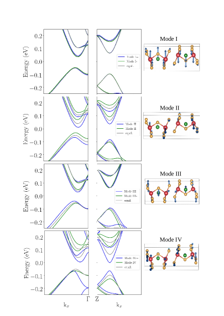
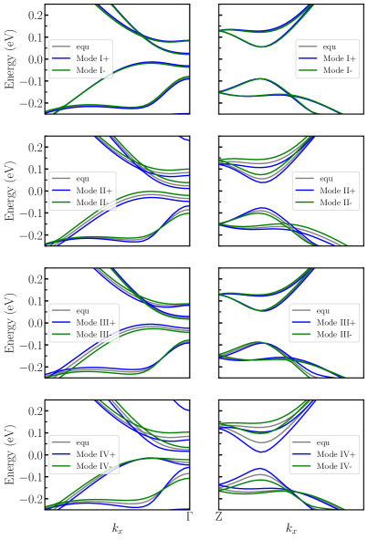
We conclude our work by demonstrating the intimate coupling between the electronic and nuclear degrees of freedom by highlighting the influence of specific phononic modes on the electronic bandstructure. Time resolved ARPES measurements by Baldini et al. find that the gap presents oscillatory behaviour under photoexcitation Baldini2020 . The authors show that the momentum integrated photoelectron intensity is dominated by 4 frequency components: 0.98 THz, 2.11 THz, 3.0 THz and 3.67 THz. The four frequencies can be identified as the frequencies of Raman active phonons and using our phonon dispersion calculation (Fig. 7a) we can identify the corresponding modes, with Mode I at 1.1 THz, Mode II at 1.9 THz, mode III at 2.9 THz and IV at 3.4 THz. We observe that the modes II and IV have B symmetry and show the characteristic shearing with respect to the Tantalum atoms around the Nickel atoms while the Modes I and III have A symmetry do not exhibit this shearing. They can be identified with the peaks 1, 2, 3 and 5 in the Raman measurements of figures 8 and 9. Mode IV mode can also be identified as the monoclinic counterpart of the B soft-mode which is unstable in the orthorhombic geometry (see Fig. 7e).
To quantify how strongly the above discussed phonons couple to the electrons, we have calculated their effect on the electronic bandstructure by displacing the atoms along the phonon eigenmodes by an amount equal to the square root of their mean-squared displacement at zero temperature for both the positive and negative direction. The resulting bandstructures using the G0W0 method are shown in Fig. 10 (see Supplementary Figure 12 for the PBE results). We see that the Modes I and III show little influence whereas both B modes have a strong impact on the electronic structure. We stress that both of these modes exhibit the characteristic shearing of the Ta atoms around the Nickel atom in chain direction, which we also observed during the structural phase transition (see Fig. 7c) . For the Mode IV the average gap between positive and negative displacement is larger than the equilibrium gap. Therefore, we expect a small increase of around meV of the bandgaps predicted in the previous section due to the coupling of this phonon to the electronic degrees of freedom.
These results, beside confirming the strong influence of phonons on the electronic structure, hint towards the possibility of modulating the electronic bandgap through an external pumping of the above phononic modes.
3 Discussion
We have shown that the orthorhombic phase of both TNSe and TNS is unstable at low temperatures and exhibits a soft phonon mode, which signals the structural transition to the monoclinic phase.
Performing electronic bandstructure calculations using different exchange correlation functionals, as well as calculations using the G0W0 approximation, we have proven that in TNSe the structural transition drives the metal to semiconducting phase transition, with an indirect bandgap that is comparable to the experimental results Lu2017 ; Lee2019 , while in TNS the semiconductive electronic nature is preserved. This demonstrates that without the structural transition the experimentally observed gap opening at the critical temperature cannot be explained. At the same time our ab-initio results show that no excitonic effects are necessary to explain the experimental evidences. Furthermore, during the structural transition a significant flattening of the valence bands is observed which is enhanced by electronic heating leading to almost flat bands which are in agreement with recently measured (pump-probe) ARPES signatures Baldini2020 .
The electronic heating shows that the bandgap never closes for increasing electronic temperatures but shows the expected renormalization effects of standard semiconductors due to the increased carrier density.
We discussed the possible origins of the structural transition in relation to the scenario of a purely electronic instability occurring at fixed ion positions and concluded that a structural distortion is required in order to observe a metal-insulator transition in TNSe. This is supported by scans of the total energy landscape and charge density as a function of the relevant distortion parameters which show no sign of an electronic instability.
Investigating the change of the electronic bandstructure for experimentally relevant phonon modes we found that the electrons tend to couple stronger to the phonon modes which displace along the chain direction and induce the characteristic shearing of the Ta atoms around the Ni atom. Especially the THz phonon mode is expected to lead to a small additional bandgap opening through the thermal occupation of this mode. We conclude that, in the low temperature phase, TNSe and TNS behave as standard semiconductors.
Methods
Computational Details
All DFT and G0W0 calculations have been performed with the Vienna Ab initio Simulation Package (VASP) Vasp1 ; Vasp2 ; Vasp3 ; Vasp4 ; Vasp5 and in the case of phonon calculations we additionally used phonopy to compute phonon dispersions phonopy . For the interpolation of the G0W0 bandstructure we have used the wannier90 package wannier90 .
All calculations have made use of the PBE pseudopotential set generated with VASP VaspPseudos .
The structural relaxations have been performed on a 24x4x6 k-mesh with an energy cutoff of 460 meV. A total free energy change of 1e-6 eV has been used as cutoff criterion which led to forces of 2.8 meV/angstrom per ion or less. The resulting input structures are shown in section 1 of the SI.
The phonon dispersion calculation has been performed using the vdw-optB88 functional and a 4x2x1 supercell with a 4x4x3 k-mesh. The post-processing has been performed with the phonopy package phonopy . The calculation of the phonon spectra at which are compared to the Raman data has been performed on a k48x4x6 mesh using a single unit cell. The calculation of the phonon overlaps as a function of the distortion parameter has been performed on a k16x8x3 mesh.
The electronic bandstructure calculations have been performed on a 24x8x6 k-mesh for the PBE functional and a 16x4x4 k-mesh for the modified Becke-Johnson and HSE hybrid functionals and the Hartree-Fock calculation. The mBJ-functional calculated self-consistently a c value of 1.2578 for the orthorhombic and a c-value of 1.2636 for the monoclinic phase of TNSe. For TNS c is 1.2620 for both structural phases. The bandstructures have been computed along the path M=, Z=, = and X=.
The G0W0 calculations have been performed on a 12x4x2 k-mesh with 160 frequencies and 1160 states with a 100 meV energy Cutoff. The Wannierization has been performed with the Wannier90 package Mostofi2014 . A convergence study of the relevant parameters for the presented G0W0 calculation can be found in the Supplementary Note 7 and Supplementary Figures 13-15.
Data Availability
The authors declare that the main data supporting the findings of this study are contained within the paper and its associated Supplementary Information. All other relevant data are available from the corresponding author upon reasonable request.
Code Availability
The VASP software package is available at https://www.vasp.at/. The open-source software packages Wannier90 is available at http://www.wannier.org/ under the GNU General Public License (v2). The open-source phonopy package is available at https://phonopy.github.io/phonopy/ under the BSD license.
Acknowledgements
We are grateful to E.Baldini, I.Mazin and Yann Gallais for enlightening discussions throughout the course of this work. We would like to thank M. Ye, G. Blumberg, K.Kim, B.J. Kim, M.J. Kim and S. Kaiser for sharing the experimental data of their Raman measurements and valuable discussions.
This work is supported by the European Research Council (ERC-2015-AdG-694097), Grupos Consolidados (IT1249-19) and the Flatiron Institute, a division of the Simons Foundation. We acknowledge funding by the Deutsche Forschungsgemeinschaft (DFG) under Germany’s Excellence Strategy - Cluster of Excellence Advanced Imaging of Matter (AIM) EXC 2056 - 390715994 and by the Deutsche Forschungsgemeinschaft (DFG, German Research Foundation) – SFB-925 – project 170620586. Support by the Max Planck Institute - New York City Center for Non-Equilibrium Quantum Phenomena is acknowledged.. S. L. acknowledges support from the Alexander von Humboldt foundation.
G. M. acknowledges support of the Swiss National Science Foundation FNS/SNF through an Ambizione grant.
Author Contributions
A.R and S.L designed the project. L.W performed the computations under the supervision of S.L. All authors discussed the computational results and contributed to the writing and revision of the manuscript.
Competing Interests
The authors declare no competing interests.
Supplementary Information
Supplementary Note 1
The bandstructures have been computed along the path M=, Z=, = and X=.
Supplementary Note 2: Total energy minimum with different functionals
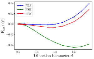
To track the total energy changes during the relaxation for different functionals we have computed the energy of the system along the structural transition. We employed again the parameter introduced in section 2.4 of the main text to parameterize the transition. The resulting total energy vs distortion graph is shown in Supplementary Figure 11. For all functionals the total energy is displayed with the orthorhombic value set 0 eV. The figure shows, that using the PBE functional has the energy minimum at slightly lower values for the distortion and the HSE has its energy minimum at stronger distortion values of . Nevertheless, a monoclinic structure is energetically more stable than the orthorhombic geometry for all investigated functionals.
Supplementary Note 3: Spin-Orbit Coupling
The results for the PBE, mBJ and HSE03 with and without Spin-Orbit Coupling (SOC) functional are shown in the Supplementary Figures 12, 13 and 14. They show that SOC leads to a bandsplitting which is most apparent on the M-Z path for all band dispersions. Note, that this band splitting is not a splitting of spin up and down states. Near the bandedge the spin orbit coupling has just a small influence on the bandstructures. Only for the monoclinic geometry of TNSe using the PBE functional changes are apparent with the bandgap halving and the becoming and direct at . A detailed comparison of the obtained bandgaps is presented in Supplementary Table 6. We conclude, that the effects of SOC are negligible for our discussion in the main text. These results are in agreement with a prior study by Sugimoto et al. Sugimoto2018 .
Supplementary Note 4: Increasing the exchange-correlation contribution in the functionals
Increasing the exchange and correlation contribution considered in either the HSE hybrid functionals or the modified-Becke-Johnson functional will lead to a bandgap opening even in the orthorhombic unit cell. In the modified Becke-Johnson (mBJ) functional the amount of exchange and correlation interaction included is controlled by the c parameter. It controls the amount of Becke-Roussel exchange Becke2006 ; Becke1989 , which approximates exact exchange effects via an effective potential, plus a screening term Tran2009 . In the HSE hybrid functionals the exact exchange contribution is calculated directly using the Kohn-Sham orbitals during the self consistent iterations. Parts of the PBE exchange interaction are replaced by the exact exchange interaction Heyd2003 . The admixture of exact and PBE exchange in the functional is controlled by the mixing parameter which is commonly set to 0.25 for the HSE functionals. Varying it we can modify the amount of exchange interaction analogously to varying the parameter in the mBJ functional. The results are shown in the Supplementary Figure 15 and Supplementary Figure 16. We see, that for values of 1.6 or higher a bandgap opens, while the system is still metallic for the self consistently calculated c-Value of 1.26. Analogously we can control the amount of exchange and correlation included in the range separated hybrid functionals. To test this we have varied the mixing parameter , while keeping the range separation parameter at 0.3. This way reproduces the result for the HSE03 functional. The resulting bandstructures can be seen in Supplementary Figure 16. The behaviour is similar to the mBJ case, with the orthorhombic cell becoming a semiconductor for values of .
Supplementary Note 5: Minimally symmetry broken electron dispersion
We used the displacement parameter as defined in section 3 of the main text to introduce a minimal distortion to the lattice (d=0.05). This procedure breaks the relevant orthorhombic lattice symmetries. If the phase transition of TNSe is fully electronic the breaking of the symmetries should already induce the metal to semiconductor transition. The result for the electronic dispersion of the symmetry broken geometry is shown in Supplementary Figure 18. We see that all bandstructures ,independent of the exchange correlation functional, do not exhibit a metal to insulator transition or a significant gap opening. In fact they agree very well with the exact orthorhombic results.
Supplementary Note 6: STS Gap Correction
In STS measurements a metal to semiconductor transition has been reported at the critical temperature for TNSe Lee2019 . The reported bandgap is 300 meV and is significantly bigger than the bandgap obtained from optics measurements of 160 meV Lu2017 . The discrepancy can be explained taking the different geometries of the investigated samples of TNSe in account. The sample used for the STS measurement exhibits an -angle of 92.5∘ and is such significantly bigger than the literature result of 90.5∘-90.7∘ Sunshine1985 ; Nakano2018 . To correct the bandgap taking this discrepancy into account, we computed the bandstructures for both our monoclinic unit cell as well as a unit cell with 92.5∘ -angle. The obtained bandgaps are 40meV for our relaxed geometry and 66 meV for the 92.5∘ geometry using the PBE functional. Taking the ratio of these two and multiplying the 300 meV experimental gap, we obtain a correction of the STS gap to 181 meV.
Supplementary Note 7: Convergence of the G0W0 calculations
We present the details of the convergence of the G0W0 calculation for the monoclinic unit cell. To display the convergence behaviour of the calculation we performed convergence studies for the number of k-Points needed in each direction, the number of unoccupied bands and the energy cutoff we have to consider for the response function calculation and size of the frequency grid of the frequency integration. It is important to note, that the energy cutoff for the response function and the number of unoccupied states are not independent convergence parameters and thus, we use the standard method and converge them simultaneously Klimes2014 . The bandstructures have been obtained via post-processing using the Wannier90 package wannier90 .
For the presented convergence studies we have employed the Density Functional Theory solution using the PBE functional as starting point. A discussion of the effect using different functionals such as the HSE hybrid functional is in the section 2.3 of the main text.
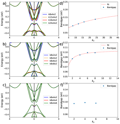
For the bandstructure convergence of TNSe with varying k-mesh we will assume that the spatial directions for the k-mesh converge independently and perform a series of calculations with varying grid size in all three directions. To measure the convergence of the bandstructure we will compute the fundamental bandgap and extrapolate using a function with , and as fitting parameters. For these k-mesh calculations we used 640 unoccupied states with a 80eV Cutoff for the response function and 160 frequency grid points in the calculation of the screened interaction. The k-meshes are , and with and are varied. The result is shown in Supplementary Figure 23. One sees, that the convergence in and along the corresponding reciprocal lattice directions converges quite fast. This is different for as the bandstructure is highly dispersive in x-direction and many grid-points are needed to sample it accurately.
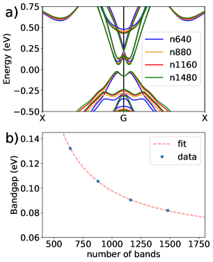
We also performed a simultaneous convergence of the energy cutoff for the response function and the number of unoccupied states. Convergence against the exact result should be in first order proportional to 1/Number of unoccupied states Klimes2014 . We have performed the convergence calculation in the standard way increasing response function cutoff and the number of included orbitals simultaneously. The given combinations are shown in Supplementary Table 8. The result of the energy convergence is presented in Supplementary Figure 24. We see, that including 1160 unoccupied states leads to a quite well converged bandgap already.
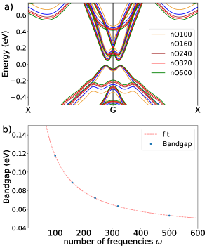
Lastly we also investigate of the convergence with increasing number of frequency grid points. This time the test setup is a k-mesh of 12x4x2 with 880 unoccupied states and a 100eV Cutoff. The result is shown in Fig 25. We see, that full convergence is only achieved for a large number of frequencies considered due to the small bandgap.
Supplementary Note 8: BSE Convergence
We also investigated the convergence behaviour of the solution of the Bethe-Salpether equation Salpeter1951 ; Sander2015 for the monoclinic phase of TNSe. We performed the BSE using the eigenenergies and screened interaction from the G0W0 calculation. The calculations show, that for all convergence parameters the excitonic binding energy decreases proportional to the bandgap. This together with the fact, that even more converged G0W0 calculations in kx tend to increase the G0W0 bandgap suggests, that for the material the excitonic binding energy does not exceed the bandgap. A detailed analysis of all relevant convergence parameters follows:
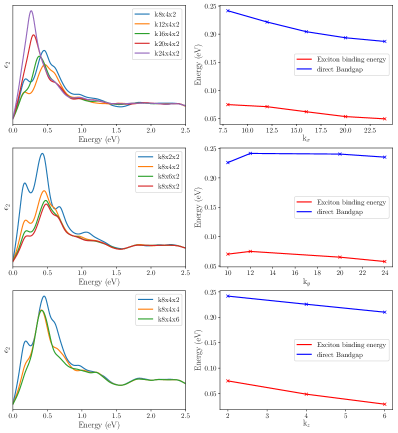
The solution of the Bethe-Salpether equation is very sensitive to the k-mesh. Thus, we investigated the solution of the BSE with an increasing k-mesh along the three different axes. We use a test setup with 160 frequencies for the calculation of the screened interaction, 640 unoccupied states (80eV cutoff) during the G0W0 calculation and include again the first 12 valence and 14 conduction bands in the BSE. The k-meshes used are kxx4x2, 8xkyx2 and 8x4xkz, where kx, ky and kz are variable and are be successively increased. The results are depicted in Supplementary Figure 26. We see, that while the dielectric function converges quickly with an increasing k-mesh in y-direction and z-direction, we need many k-points in kx direction to obtain we reasonable result. The reason is, that the bandgap minimum is shifted slightly toward x-direction after the G0W0 calculation and therefore only very dense k-meshes can sample the highly dispersive energies in x-direction.
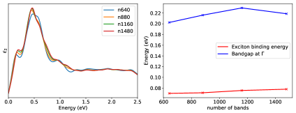
Secondly, we investigate the effect onto the BSE calculation for an increasing cutoff in the G0W0 calculation and an increasing number of unoccupied states. The test setup is working with a 12x4x2 k-mesh, 160 frequencies for the calculation of the screened interaction and including the first 12 valence and 14 conduction band states in the BSE. We employed the Tamm-Dancoff approximation Dancoff1950 ; Sander2015 . The results are depicted in Supplementary Figure 27. Using 880 unoccupied states with a 80eV cutoff already gives a well converged dielectric function and excitonic binding energies.
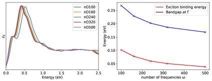
The third convergence parameter we investigate is the effect of including an increasing number of frequencies in the computation of the screened interaction onto the result of the Bethe-Salpeter equation. The test setup is using a 12x4x2 k-mesh, 640 unoccupied states and the first 12 valence and 14 conduction band states in the BSE. The results is depicted in Supplementary Figure 28. We see, that the BSE solution converges quite fast with the number of frequencies included in the calculation of the screened interaction. The dielectric function only obtains a rigid shift, which can be explained by the decreasing bandgap of the underlying G0W0 bandstructure calculation.
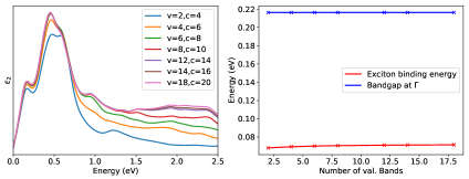
Lastly, we show the BSE convergence properties with an increasing number of valence and conduction bands included in the BSE calculation. The test setup includes a 12x4x2 k-mesh, 880 unoccupied states, a 80 eV cutoff and 160 frequencies in the calculation of the screened interaction. The number of valence (v) and conduction bands (c) included is varied. The convergence of the dielectric function and the eigenvalues of the BSE solution is displayed in the Supplementary Figure 29. We see, that we always obtain well converged eigenvalues, but need to include at least the first 12 valence and the first 14 conduction bands around the Fermi level to obtain a fully converged dielectric function. The excitonic eigenvalues are already very well converged only the first valence and conduction bands.
| a (in ) | b (in ) | c (in ) | |
|---|---|---|---|
| Experiment Nakano2018 | 3.492 | 12.814 | 15.649 |
| vdW-optB88 | 3.517 | 12.982 | 15.776 |
| vdW-optPBE | 3.532 | 13.325 | 15.845 |
| PBE | 3.510 | 14.160 | 15.776 |
| a (in ) | b (in ) | c (in ) | |
|---|---|---|---|
| ExperimentNakano2018_2 | 3.503 | 12.870 | 15.677 |
| vdW-optB88 | 3.512 | 12.993 | 15.771 |
| vdW-optPBE | 3.526 | 13.252 | 15.834 |
| PBE | 3.504 | 14.190 | 15.762 |
| a (in ) | b (in ) | c (in ) | |
|---|---|---|---|
| ExperimentSunshine1985 | 3.415 | 12.146 | 15.097 |
| orthorhombic | 3.430 | 12.200 | 15.203 |
| monoclinic | 3.428 | 12.223 | 15.203 |
| lattice vector | x (in ) | y (in ) | z (in ) |
|---|---|---|---|
| a | 3.51177786 | 0.00000000 | 0.00000000 |
| b | 1.75588893 | 6.49659343 | 0.00000000 |
| c | 0.00000000 | 0.00000000 | 15.77141641 |
| species | a | b | c |
| Ta | 0.22143275 | 0.55713450 | 0.88896088 |
| Ta | 0.22143275 | 0.55713450 | 0.61103912 |
| Ta | 0.77856725 | 0.44286550 | 0.11103912 |
| Ta | 0.77856725 | 0.44286550 | 0.38896088 |
| Ni | 0.70190352 | 0.59619297 | 0.75000000 |
| Ni | 0.29809648 | 0.40380703 | 0.25000000 |
| Se | 0.58116235 | 0.83767530 | 0.86174128 |
| Se | 0.58116235 | 0.83767530 | 0.63825872 |
| Se | 0.41883765 | 0.16232470 | 0.13825872 |
| Se | 0.41883765 | 0.16232470 | 0.36174128 |
| Se | 0.14695064 | 0.70609873 | 0.04873952 |
| Se | 0.14695064 | 0.70609873 | 0.45126048 |
| Se | 0.85304936 | 0.29390127 | 0.95126048 |
| Se | 0.85304936 | 0.29390127 | 0.54873952 |
| Se | 0.32729988 | 0.34540023 | 0.75000000 |
| Se | 0.67270012 | 0.65459977 | 0.25000000 |
| lattice vector | x (in ) | y (in ) | z (in ) |
|---|---|---|---|
| a | 3.5172791481 | 0.0000000000 | 0.0000000000 |
| b | 1.7642919084 | 6.4903780477 | 0.0000000000 |
| c | -0.1695581062 | -0.0018790259 | 15.7763685968 |
| species | a | b | c |
| Ta | 0.788009744 | 0.446403261 | 0.888662426 |
| Ta | 0.765747213 | 0.446396149 | 0.611343122 |
| Ta | 0.209582861 | 0.558275853 | 0.111357977 |
| Ta | 0.231832330 | 0.558274801 | 0.388645515 |
| Ni | 0.297194687 | 0.407655269 | 0.750000961 |
| Ni | 0.701051209 | 0.596787458 | 0.250006008 |
| Se | 0.411119367 | 0.165767233 | 0.861499543 |
| Se | 0.424071823 | 0.165757101 | 0.638461393 |
| Se | 0.586395710 | 0.838882702 | 0.138539629 |
| Se | 0.573462842 | 0.838897364 | 0.361493392 |
| Se | 0.859540334 | 0.295478962 | 0.048418035 |
| Se | 0.845322448 | 0.295464258 | 0.451556475 |
| Se | 0.137960710 | 0.709232641 | 0.951592761 |
| Se | 0.152210287 | 0.709218409 | 0.548427477 |
| Se | 0.670947177 | 0.658753928 | 0.750003802 |
| Se | 0.327025141 | 0.345806896 | 0.249991137 |
| TNSe, ortho | TNSe, mono | TNSe, ortho,SOC | TNSe, mono, SOC | ||
| PBE | metallic | 40 meV | metallic | 18 meV (-55%) | |
| mBJ | metallic | 101 meV | metallic | 120 meV (+18%) | |
| HSE03 | metallic | 183 meV | metallic | 179 meV (-2%) | |
| TNS, ortho | TNS, mono | TNS, ortho,SOC | TNS, mono, SOC | ||
| PBE | metallic | 102 meV | metallic | 102 meV (+0%) | |
| mBJ | 42 meV | 151 meV | 98 meV (+133%) | 178 meV (+18%) | |
| HSE03 | 248 meV | 352 meV | 250 meV (+1%) | 362 meV (+3%) |
| Mode | Orthorhombic (THz) | Monoclinic (THz) |
|---|---|---|
| 1 | -2.581 | 0.000 |
| 2 | 0.000 | 0.000 |
| 3 | 0.000 | 0.000 |
| 4 | 0.000 | 1.156 |
| 5 | 0.761 | 1.224 |
| 6 | 1.160 | 1.543 |
| 7 | 1.224 | 1.703 |
| 8 | 1.670 | 1.969 |
| 9 | 1.890 | 2.084 |
| 10 | 2.580 | 2.668 |
| 11 | 2.693 | 3.117 |
| 12 | 3.107 | 3.331 |
| 13 | 3.136 | 3.403 |
| 14 | 3.299 | 3.628 |
| 15 | 3.370 | 3.775 |
| 16 | 3.430 | 4.160 |
| 17 | 3.567 | 4.255 |
| 18 | 3.920 | 4.397 |
| 19 | 4.255 | 4.679 |
| 20 | 4.393 | 4.966 |
| 21 | 4.578 | 5.382 |
| 22 | 4.694 | 5.675 |
| 23 | 6.410 | 6.400 |
| 24 | 7.338 | 7.159 |
| 25 | 7.657 | 7.403 |
| 26 | 7.701 | 7.476 |
| 27 | 7.785 | 7.520 |
| 28 | 7.817 | 7.585 |
| 29 | 7.823 | 8.025 |
| 30 | 7.911 | 8.029 |
| 31 | 7.967 | 8.093 |
| 32 | 8.170 | 8.134 |
| 33 | 8.183 | 8.259 |
| 34 | 8.214 | 8.439 |
| 35 | 8.490 | 8.495 |
| 36 | 8.668 | 8.686 |
| 37 | 8.733 | 8.777 |
| 38 | 9.000 | 9.311 |
| 39 | 9.313 | 9.539 |
| 40 | 9.574 | 9.715 |
| 41 | 9.691 | 9.765 |
| 42 | 9.960 | 9.958 |
| 43 | 10.142 | 10.187 |
| 44 | 10.174 | 10.242 |
| 45 | 11.362 | 11.451 |
| 46 | 11.397 | 11.459 |
| 47 | 11.477 | 11.544 |
| 48 | 11.536 | 11.571 |
| cutoff (eV) | orbitals |
|---|---|
| 60 | 640 |
| 80 | 880 |
| 100 | 1160 |
| 120 | 1480 |
References
- \bibcommenthead
- (1) Kohn, W. Excitonic phases. Phys. Rev. Lett. 19, 439–442 (1967) .
- (2) Jérome, D., Rice, T. M. & Kohn, W. Excitonic Insulator. Phys. Rev. 158 (2), 462–475 (1967) .
- (3) Mott, N. F. The transition to the metallic state. Philos. Mag. 6 (62), 287–309 (1961) .
- (4) Keldysh, L. V. & Kozlov, A. N. Collective properties of excitons in semiconductors. Sov. Phys. JETP 27, 978 (1968) .
- (5) Halperin, B. I. & Rice, T. M. Possible anomalies at a semimetal-semiconductor transistion. Rev. Mod. Phys. 40, 755–766 (1968) .
- (6) Kozlov, A. The metal-dielectric divalent crystal phase transition. Sov. Phys. JETP 21, 790 (1965) .
- (7) Cercellier, H. et al. Evidence for an excitonic insulator phase in . Phys. Rev. Lett. 99, 146403 (2007) .
- (8) Kogar, A. et al. Signatures of exciton condensation in a transition metal dichalcogenide. Science 358 (6368), 1314–1317 (2017) .
- (9) Bucher, B., Steiner, P. & Wachter, P. Excitonic insulator phase in . Phys. Rev. Lett. 67, 2717–2720 (1991) .
- (10) Ma, L. et al. Strongly correlated excitonic insulator in atomic double layers. Nature 598 (7882), 585–589 (2021) .
- (11) Jia, Y. et al. Evidence for a monolayer excitonic insulator. Nature Physics 18 (1), 87–93 (2022) .
- (12) Varsano, D., Palummo, M., Molinari, E. & Rontani, M. A monolayer transition-metal dichalcogenide as a topological excitonic insulator. Nat. Nanotechnol. 15 (5), 367–372 (2020) .
- (13) Gupta, S., Kutana, A. & Yakobson, B. I. Heterobilayers of 2d materials as a platform for excitonic superfluidity. Nat. Commun. 11 (1), 2989 (2020) .
- (14) Varsano, D. et al. Carbon nanotubes as excitonic insulators. Nat. Commun. 8 (1), 1461 (2017) .
- (15) Li, Z. et al. Possible excitonic insulating phase in quantum-confined sb nanoflakes. Nano Lett. 19 (8), 4960–4964 (2019) .
- (16) Li, J. I. A., Taniguchi, T., Watanabe, K., Hone, J. & Dean, C. R. Excitonic superfluid phase in double bilayer graphene. Nat. Phys. 13 (8), 751–755 (2017) .
- (17) Perali, A., Neilson, D. & Hamilton, A. R. High-temperature superfluidity in double-bilayer graphene. Phys. Rev. Lett. 110, 146803 (2013) .
- (18) Hu, Y., Venderbos, J. W. F. & Kane, C. L. Fractional excitonic insulator. Phys. Rev. Lett. 121, 126601 (2018) .
- (19) Du, L. et al. Evidence for a topological excitonic insulator in inas/gasb bilayers. Nat. Commun. 8 (1), 1971 (2017) .
- (20) Ataei, S. S., Varsano, D., Molinari, E. & Rontani, M. Evidence of ideal excitonic insulator in bulk mos(2) under pressure. P. Natl. Acad. Sci. USA 118 (13), e2010110118 (2021) .
- (21) Kaneko, T., Toriyama, T., Konishi, T. & Ohta, Y. Orthorhombic-to-monoclinic phase transition of Ta2NiSe5 induced by the bose-einstein condensation of excitons. Phys. Rev. B 87, 035121 (2013) .
- (22) Wakisaka, Y. et al. Excitonic insulator state in probed by photoemission spectroscopy. Phys. Rev. Lett. 103, 026402 (2009) .
- (23) Seki, K. et al. Excitonic bose-einstein condensation in above room temperature. Phys. Rev. B 90, 155116 (2014) .
- (24) Watson, M. D. et al. Band hybridization at the semimetal-semiconductor transition of enabled by mirror-symmetry breaking. Phys. Rev. Research 2, 013236 (2020) .
- (25) Tang, T. et al. Non-coulomb strong electron-hole binding in revealed by time- and angle-resolved photoemission spectroscopy. Phys. Rev. B 101, 235148 (2020) .
- (26) Lu, Y. F. et al. Zero-gap semiconductor to excitonic insulator transition in Ta2NiSe5. Nat. Commun. 8 (1) (2017) .
- (27) Lee, J. et al. Strong interband interaction in the excitonic insulator phase of . Phys. Rev. B 99, 075408 (2019) .
- (28) Baldini, E. et al. The spontaneous symmetry breaking in Ta2NiSe5 is structural in nature Preprint at https://arxiv.org/abs/2007.02909 (2020) .
- (29) Kaneko, T., Toriyama, T., Konishi, T. & Ohta, Y. Electronic structure of Ta2NiSe5 as a candidate for excitonic insulators. J. Phys. Conf. Ser. 400 (3), 032035 (2012) .
- (30) Nakano, A. et al. Antiferroelectric distortion with anomalous phonon softening in the excitonic insulator . Phys. Rev. B 98, 045139 (2018) .
- (31) Di Salvo, F. et al. Physical and structural properties of the new layered compounds Ta2NiS5 and Ta2NiSe5. J. Less-Common Met. 116 (1), 51–61 (1986) .
- (32) Sunshine, S. A. & Ibers, J. A. Structure and physical properties of the new layered ternary chalcogenides tantalum nickel sulfide (Ta2NiS5) and tantalum nickel selenide (Ta2NiSe5). Inorg. Chem. 24 (22), 3611–3614 (1985) .
- (33) Ye, M. et al. Lattice dynamics of the excitonic insulator . Phys. Rev. B 104, 045102 (2021) .
- (34) Mu, K. et al. Electronic structures of layered Ta2NiS5 single crystals revealed by high-resolution angle-resolved photoemission spectroscopy. J. Mater. Chem. C 6, 3976–3981 (2018) .
- (35) Mazza, G. et al. Nature of symmetry breaking at the excitonic insulator transition: . Phys. Rev. Lett. 124, 197601 (2020) .
- (36) Subedi, A. Orthorhombic-to-monoclinic transition in due to a zone-center optical phonon instability. Phys. Rev. Materials 4, 083601 (2020) .
- (37) Klimeš, J. c. v., Bowler, D. R. & Michaelides, A. Van der waals density functionals applied to solids. Phys. Rev. B 83, 195131 (2011) .
- (38) Klimeš, J., Bowler, D. R. & Michaelides, A. Chemical accuracy for the van der Waals density functional. J. Phys. Condens. Mat. 22 (2) (2010) .
- (39) Perdew, J. P., Burke, K. & Ernzerhof, M. Generalized gradient approximation made simple. Phys. Rev. Lett. 77, 3865–3868 (1996) .
- (40) Tran, F. & Blaha, P. Accurate band gaps of semiconductors and insulators with a semilocal exchange-correlation potential. Phys. Rev. Lett. 102, 226401 (2009) .
- (41) Becke, A. D. & Johnson, E. R. A simple effective potential for exchange. J. Chem. Phys. 124 (22), 221101 (2006) .
- (42) Becke, A. D. & Roussel, M. R. Exchange holes in inhomogeneous systems: A coordinate-space model. Phys. Rev. A 39, 3761–3767 (1989) .
- (43) Heyd, J., Scuseria, G. E. & Ernzerhof, M. Hybrid functionals based on a screened coulomb potential. J. Chem. Phys. 118 (18), 8207–8215 (2003) .
- (44) Sugimoto, K., Nishimoto, S., Kaneko, T. & Ohta, Y. Strong coupling nature of the excitonic insulator state in . Phys. Rev. Lett. 120, 247602 (2018) .
- (45) Li, L. et al. Strong in-plane anisotropies of optical and electrical response in layered dimetal chalcogenide. ACS Nano 11 (10), 10264–10272. PMID: 28901748 (2017) .
- (46) Larkin, T. I. et al. Giant exciton fano resonance in quasi-one-dimensional . Phys. Rev. B 95, 195144 (2017) .
- (47) van Schilfgaarde, M., Kotani, T. & Faleev, S. Quasiparticle self-consistent gw theory. Phys. Rev. Lett. 96, 226402 (2006) .
- (48) Onida, G., Reining, L. & Rubio, A. Electronic excitations: density-functional versus many-body green’s-function approaches. Rev. Mod. Phys. 74, 601–659 (2002) .
- (49) Hybertsen, M. S. & Louie, S. G. First-principles theory of quasiparticles: Calculation of band gaps in semiconductors and insulators. Phys. Rev. Lett. 55, 1418–1421 (1985) .
- (50) Hybertsen, M. S. & Louie, S. G. Electron correlation in semiconductors and insulators: Band gaps and quasiparticle energies. Phys. Rev. B 34, 5390–5413 (1986) .
- (51) Hedin, L. New method for calculating the one-particle green’s function with application to the electron-gas problem. Phys. Rev. 139, A796–A823 (1965) .
- (52) Salpeter, E. E. & Bethe, H. A. A relativistic equation for bound-state problems. Phys. Rev. 84, 1232–1242 (1951) .
- (53) Sander, T., Maggio, E. & Kresse, G. Beyond the tamm-dancoff approximation for extended systems using exact diagonalization. Phys. Rev. B 92, 045209 (2015) .
- (54) Spataru, C. D., Benedict, L. X. & Louie, S. G. Ab initio calculation of band-gap renormalization in highly excited gaas. Phys. Rev. B 69, 205204 (2004) .
- (55) Beni, G. & Rice, T. M. Theory of electron-hole liquid in semiconductors. Phys. Rev. B 18, 768–785 (1978) .
- (56) Kim, K. et al. Direct observation of excitonic instability in Ta2NiSe5. Nat. Commun. 12 (1), 1969 (2021) .
- (57) Nakano, A. et al. Pressure-induced coherent sliding-layer transition in the excitonic insulator Ta2NiSe5. IUCrJ 5 (2), 158–165 (2018) .
- (58) Volkov, P. A. et al. Critical charge fluctuations and emergent coherence in a strongly correlated excitonic insulator. NPJ Quantum Mater. 6 (1), 52 (2021) .
- (59) Volkov, P. A. et al. Failed excitonic quantum phase transition in . Phys. Rev. B 104, L241103 (2021) .
- (60) Kim, M.-J. et al. Phononic soft mode and strong electronic background behavior across the structural phase transition in the excitonic insulator Ta2NiSe5 (with erratum) Preprint at https://arxiv.org/abs/2007.01723 (2021) .
- (61) Zhou, J.-J., Hellman, O. & Bernardi, M. Electron-phonon scattering in the presence of soft modes and electron mobility in perovskite from first principles. Phys. Rev. Lett. 121, 226603 (2018) .
- (62) Kresse, G. & Hafner, J. Ab initio molecular dynamics for liquid metals. Phys. Rev. B 47, 558–561 (1993) .
- (63) Kresse, G. & Furthmüller, J. Efficient iterative schemes for ab initio total-energy calculations using a plane-wave basis set. Phys. Rev. B 54, 11169–11186 (1996) .
- (64) Kresse, G. & Furthmüller, J. Efficiency of ab-initio total energy calculations for metals and semiconductors using a plane-wave basis set. Comp. Mater. Sci. 6 (1), 15–50 (1996) .
- (65) Kresse, G. & Hafner, J. Norm-conserving and ultrasoft pseudopotentials for first-row and transition elements. J. Phys. Condens. Mat. 6 (40), 8245–8257 (1994) .
- (66) Kresse, G. & Joubert, D. From ultrasoft pseudopotentials to the projector augmented-wave method. Phys. Rev. B 59, 1758–1775 (1999) .
- (67) Togo, A. & Tanaka, I. First principles phonon calculations in materials science. Scripta Mater. 108, 1–5 (2015) .
- (68) Mostofi, A. A. et al. An updated version of wannier90: A tool for obtaining maximally-localised wannier functions. Comput. Phys. Commun. 185 (8), 2309 – 2310 (2014) .
- (69) Kresse, G. & Joubert, D. From ultrasoft pseudopotentials to the projector augmented-wave method. Phys. Rev. B 59, 1758–1775 (1999) .
- (70) Mostofi, A. A. et al. An updated version of wannier90: A tool for obtaining maximally-localised wannier functions. Comput. Phys. Commun. 185 (8), 2309–2310 (2014) .
- (71) Klimeš, J. c. v., Kaltak, M. & Kresse, G. Predictive calculations using plane waves and pseudopotentials. Phys. Rev. B 90, 075125 (2014) .
- (72) Dancoff, S. M. Non-adiabatic meson theory of nuclear forces. Phys. Rev. 78, 382–385 (1950) .