Laser-induced electron emission from Au nanowires: a probe for orthogonal polarizations
Abstract
Photoelectron field emission, induced by femtosecond laser pulses focused on metallic nanotips, provides spatially coherent and temporally short electron pulses. Properties of the photoelectron yield give insight into both the material properties of the nanostructure and the exciting laser focus. Ultralong nanoribbons, grown as a single crystal attached to a metallic taper, are sources of electron field emission that have not yet been characterized. In this report, photoemission from gold nanoribbon samples is studied and compared to emission from tungsten and gold tips. We observe that the emission from sharp tips generally depends on one transverse component of the exciting laser field, while the emission of a blunted nanoribbon is found to be sensitive to both components. We propose that this property makes photoemission from nanoribbons a candidate for position-sensitive detection of the longitudinal field component in a tightly focused beam.
A consequence of tightly focusing a beam of light is that the beam will become longitudinally polarized near the focus.Richards and Wolf (1959); Cicchitelli, Hora, and Postle (1990); Dorn, Quabis, and Leuchs (2003) Longitudinally polarized beams are desirable because their focal widths can be below the diffraction limit, and the longitudinal component of the electric field does not contribute to the energy flow along the direction of beam propagation.Wang et al. (2008); Yu et al. (2016) These features find applications in high-resolution optical microscopy,Yoshiki et al. (2007); Terakado, Watanabe, and Kano (2009) optical data storage,Kim et al. (2007) particle trapping,Zhan (2004, 2012) charged particle acceleration,Gupta et al. (2007) material ablation,Hnatovsky et al. (2011) and pushing the high-intensity frontier. The longitudinal field component of a laser focus has been characterized in situ by atomic fluorescenceNovotny et al. (2001) and near-field microscopy,Yu et al. (2016) and ex situ via imaging of material damageHnatovsky et al. (2011) and atomic force microscopy of thin film deformation.Gilbert et al. (2006) As the in situ methods of characterizing the longitudinal field are limited by intensity or to a resonant wavelength, a flexible alternative would be preferable.
Photoelectron field emission, induced by focusing femtosecond laser pulses onto sharp metallic tapers with nanometric radii of curvature, Hommelhoff et al. (2006); Ropers et al. (2007); Barwick et al. (2007) has a broad range of applications. Temporally short electron wave packetsKrüger, Schenk, and Hommelhoff (2011) with high spatial coherenceHommelhoff et al. (2009); Ehberger et al. (2015) can be achieved with moderate intensities. Tip sources have thus been integrated into electron microscopes to obtain sub-micron spatial resolution with femtosecond timing.Barwick, Flannigan, and Zewail (2009); Gulde et al. (2014); Piazza et al. (2015) Femtosecond electron pulses have been used to study fundamental quantum mechanics, as in testing the existence of forces in the Aharonov-Bohm effect,Caprez, Barwick, and Batelaan (2007) and observing diffraction in time.Krüger, Schenk, and Hommelhoff (2011); Krüger et al. (2012) Electron emission from nanotips is obtained for a range of laser intensities and wavelengths.Herink, Wimmer, and Ropers (2014); Förster et al. (2016); Huang et al. (2017) Nanotip emission might then provide an alternative for characterizing the longitudinal component of a laser focus. However, as nanotip emission is dominated by a single transverse component of the polarization of the exciting field, it has not yet been utilized as a detector of longitudinal fields.
Ultralong gold nanoribbons,Basnet et al. (2017) grown by the method of directed electrochemical nanowire assembly (DENA),Ozturk et al. (2007); Flanders (2012)are as of yet unstudied sources for ultrafast electron photoemission. The DENA methodology results in single-crystalline samples, as confirmed by electron diffraction. Previous studies into the optical damage threshold of similar nanowire samples indicated that single-crystalline gold nanowires could tolerate high laser pulse peak intensities before melting, but that they exhibited long cooling times.Summers et al. (2014) From these studies, the exchange and dissipation of heat between the nanowire electrons and the crystalline lattice could be modelled. A logical next step would then be to characterize electrons emitted from nanoribbons in response to ultrashort pulse illumination. Photoelectron emission is known to carry information on material effects, such as plasmonic dynamics and laser heating.Vogelsang et al. (2015); Kealhofer et al. (2012) Temporally short electron pulses have been observed from plasmonic nanostructures,Irvine, Dechant, and Elezzabi (2004); Dombi et al. (2010) and the photoemission yield has been used as a sensitive probe of the plasmonic field enhancement from nanostructures.Rácz et al. (2017) We measured photoelectron emission from nanoribbons in an attempt to determine their plasmonic or thermal properties.Vogelsang et al. (2015); Rácz et al. (2017); Kealhofer et al. (2012) In the following, nanoribbon samples are characterized by photoelectron emission and compared to standard single-crystalline gold and tungsten samples. The resulting photoelectron emission spectra reveal that nanoribbons can be employed as position- and polarization-sensitive detectors within a laser focus, providing a potential in situ sub-wavelength probe for longitudinal polarization.
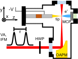
A schematic for the system used to characterize tip samples is given in Fig. 1.

The intensity of the output from a Ti:Saph oscillator (Spectra Physics Tsunami, repetition rate, central wavelength, pulse width) is controlled by a variable attenuator (VA), which consists of a plate and a Brewster window. The attenuated beam is split into a pump and a probe beam by a balanced Mach-Zehnder interferometer (IFM). Photoelectron emission is observed in pump/probe and single beam experiments. The time delay between pump and probe pulses, , can be varied from to manually by a micrometer. The additive ratio, measured as a function of the delay , is obtained by dividing the emission rate measured with both pump and probe pulses delivered to the samples by the sum of the individual rates due to the pump and probe pulses. A second plate (HWP) rotates the polarization of both beams prior to delivery to the experimental chamber. A rotational stepper motor is used to scan the beam power and the polarization.
The experimental chamber, which is detailed in Ref. Barwick et al., 2007, is maintained at Torr. The beams are focused within the chamber by an off-axis parabolic mirror (OAPM) to a full-width half maximum of . A 3-axis stage, coupled to the chamber by flexible bellows, positions tip samples into the focus. Mounted tip samples were biased at , as this was lower than the threshold for Fowler-Nordheim field emission. Electrons were collimated through two apertures before being detected by a microchannel plate (MCP).
Electron pulses from the MCP were amplified and discriminated. Discriminator pulses were counted by a multichannel scaler, and used as the start trigger for a time-to-amplitude converter (TAC). The output reference signal from the Ti:Saph oscillator was used as the TAC stop trigger to measure the arrival time of electrons. Timing spectra were obtained by sending the TAC output pulses to a multichannel analyzer (MCA).
Nanoribbon samples were prepared using the DENA methodology. Ozturk et al. (2007); Flanders (2012) Nanoribbon samples are reported to have a thickness of , and widths ranging from – along the length of the wire. The tip can have a radius of curvature of .Basnet et al. (2017) These dimensions can be tailored during the growth process to make nanoribbons that are well-suited for photoemission.
In order to distinguish which photoemission properties arise due to the material or geometry of the nanoribbon samples, single-crystal tungsten (W) and gold (Au) tips were prepared for comparison. Samples of W wire ( diameter) were annealedGreiner and Kruse (2007), and then etched via the lamella drop-off method.Müller et al. (1999) Au wire samples (% purity, Ted Pella, diameter) were annealedRoy, Williams, and Mingard (2010), and then etched as according to Refs. Gingery and Bühlmann, 2007; Eligal et al., 2009.
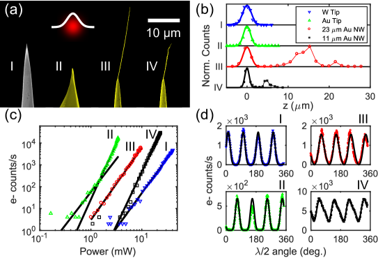
The tip and nanoribbon samples were mounted to SEM pin stubs with silver paste. SEM images of the samples are given in Fig. 2(a) along with plots of the beam focus (red) and intensity profile (white) as measured by photoemission. From left to right is shown W (I), Au (II), an undamaged Au nanoribbon (III), and an Au nanoribbon (IV) obtained after the nanoribbon was blunted during pump/probe experiments. Images were taken before and after experimental characterization to determine the extent of damage due to laser illumination.
Photoemission data from single-beam experiments are shown in Fig. 2(b)–(d). In Fig. 2(b), the emission rate is shown as samples were translated through the laser focus. The W (I) and Au (II) tip samples show emission localized at the tip apex only, while the nanoribbon samples (III and IV) can emit from multiple locations along their length. This feature confirmed that a nanoribbon remained attached to the Au substrate after imaging and transfer to the experimental chamber. Thin lines between data points serve as a guide to the eye. Fig. 2(c) shows the dependence of electron yield on the average power of the beam, plotted on a log-log scale. The value, , of the power dependence (), is often used to identify the emission process of a tip. The W tip and nanoribbon have slopes of , while the Au tip is found to have a slope of for low power, and for higher power. Such behavior, that is, the increase in power law slope with increasing laser power, has been observed in W tips and studies of above threshold photoemission.Barwick et al. (2007); Schenk, Krüger, and Hommelhoff (2010) The nanoribbon has a slope of . With these values of , the position dependence of the samples in Fig. 2 (b) can be fit with a gaussian function to determine the size of the focal waist (bold lines). The focal waist has a fitted full width at half maximum of from the W data. Fig. 2(d) shows the variation of emission rate as the polarization of the beam is rotated by a plate. The high contrast spaced peaks in the tip samples and nanoribbon support that the sample geometry is well-defined with respect to the laser polarization in the focus, and that the emission process is dominated by a preferred laser polarization. The broadened

peaks and reduced contrast of the nanoribbon electron yield (IV) indicate that the emission process depends on both transverse components of the exciting field. A feature consistent with multiphoton emission is that the power law slope, , will agree with the polarization dependence on the emission rate. The emission rate is in a multiphoton emission model, where is the polarization of the laser relative to the tip direction. The W and Au polarization data agree with a fit with , while both nanoribbon samples require a combination of and . This peculiarity of both nanoribbon samples indicates a deviation from typical multiphoton emission.
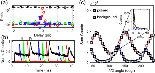
Pump/probe and single beam experiments with the TAC/MCA configuration revealed the timing features of electron emission. The additive ratio of emission from the samples is plotted in Fig. 3(a) as a function of . The polarization of the focus was chosen for the optimum electron yield from each sample. A ratio of 1 indicates that the emission yield from the probe pulses are independent from the pump pulses. A ratio significantly greater than 1 indicates emission processes that are slower than the time delay between pulses.Barwick et al. (2007) When the delay is shorter than the pulse duration, the additive ratio can vary due to interference between the pulses. The W tip (blue triangles), Au tip (green triangles), and nanoribbon all have additive ratios that are close to 1 when the pulse delay is outside of the interference window, so the emission processes are as fast as the laser pulse duration and thus prompt. The nanoribbon (black squares) has an average additive ratio of 14.9 for delays longer than the pump/probe interference window, therefore the process is not prompt. Measurement of the ratio for delays with high constructive interference were avoided to prevent damage to the Au tip and nanoribbon samples.
Normalized time spectra of electron emission from tip samples are plotted in Fig. 3(b). Shown, grouped from left to right, are the spectra from the W tip (blue line), Au tip (green line), nanoribbon (red line), and the nanoribbon (black line). The peak separation for each sample shows the pulse separation of the oscillator. Sharp peaks indicate pulsed electron emission, while sustained signal after the laser pulse indicates background emission. The nanoribbon has a significant background as compared to the other samples, indicating that electron emission is continuing after the exciting laser pulse is gone. The emission process of the nanoribbon is therefore ruled out as purely multiphoton, and is likely due to both multiphoton and laser heating of the nanoribbon structure.
To further investigate this feature, the pulsed and background contributions to emission from the nanoribbon are plotted as a function of angle in Fig. 3(c).

Time spectra were recorded for each angle. The process for dividing each spectrum into pulsed and background contributions is illustrated in the inset of Fig. 3(c), which shows a portion of the time spectrum taken at angle of . The red hatched region of the inset indicates the pulsed contribution, and the blue hatched region indicates the background. The background regions are defined by taking linear fits to the tails of the timing spectra, and extending those fits to the rising edges of the timing peaks. This procedure is performed for two oscillator periods. The counts in the background regions are summed, giving the data points marked by the blue hatched squares. The background contributions are then subtracted from the total counts in each spectrum. This results in the data points marked by the red hatched squares. The maximum emission for the background process occurs at a angle that is shifted relative to the pulsed process. For example, for a angle of , the photoemission signal is dominated by the pulsed process, as the number of counts in the tails of the electron time of flight spectra is low. For a angle of , the photoemission signal is dominated by the background process, which is marked by a comparatively high number of counts in the delayed tail of the electron time of flight spectrum. The explanation for the variation in electron signal is likely due to the nanoribbon absorbing more of the incident laser pulse energy at , and less at . The higher degree of energy absorption in the nanoribbon requires a higher degree of energy dissipation, which occurs by an additional process–thermal dissipation–that is much slower than multiphoton-driven processes. This interpretation is consistent with the results of Ref. Kealhofer et al., 2012, which demonstrated polarization control of thermally enhanced photoemission from nanotips. The polarization control of these multiphoton (pulsed) and thermal (background) processes indicates that they respond to different components of the laser field in the focus.
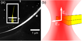
Ultralong Au nanoribbons are unique nanostructures for the study of electron, thermal, and plasmonic transport by laser-induced electron emission. Previous work indicated that nanoribbons are resilient to damage by laser intensities on the order of ,Summers et al. (2014) but we found that damage can occur with lower intensities. This observation resulted in the nanoribbon, which differed from the original nanoribbon by having a less defined apex. An immediate consequence of the laser damage to the nanoribbon was that the shorter nanoribbon required higher incident laser power to emit, which is evident in Fig. 2(c). The change in the nanoribbon’s apex geometry also coincided with emission from the nanoribbon being superadditive for emission rates similar to the other samples. The superadditive emission in pump/probe experiments was accompanied by delayed tails in the photoelectron time of flight spectra in the nanoribbon. Superadditive and delayed emission are not consistent with plasmon-induced field emission, as plasmonic emission is reported to have a standard pump/probe cross-correlation and thus is as fast as the exciting laser pulses.Dombi et al. (2010); Vogelsang et al. (2015) Such tails were not observed at the nanoribbon apex before it was damaged. These features, the superadditive emission and the delayed arrival times, are consistent with the nanoribbon being more susceptible to laser heating than the nanoribbon. The higher susceptibility to heating made the nanoribbon sensitive to both transverse components of the focused laser field, as shown in Fig. 3(c). The sensitivity to both transverse components of the focused field is a unique feature of the thermal emission of the nanoribbon that was not observed in W or Au tips. The cone structure of the nanotip samples leads to much faster cooling times than the nanoribbon samples. This suggests that a tailored nanoribbon could be oriented to probe other polarization components in a focus as well. A schematic for an oriented nanoribbon as a probe of the longitudinal component of a focused non-paraxial beam is given in Fig. 4.

Shown in Fig. 4(a) is a high-resolution SEM image of a nanoribbon and our nanoribbon as the inset. The nanoribbon is twisted in the high-resolution image to highlight its shape. With the nanoribbon oriented as shown in Fig. 4(b), the broad side of the nanoribbon would heat depending on the strength of the longitudinal component of the exciting field, , and the delayed electron yield would therefore depend on , while the peaked electron yield could depend on a combination of the transverse component, , and also . The capability to distinguish the slow thermal electron yield at the nanoribbon apex makes electron emission from a nanoribbon a subwavelength probe of orthogonal polarizations.
Acknowledgements.
We gratefully acknowledge funding by NSF EPSCoR NE-KS Track-II, Award No. EPS 1430519, and NSF grant No. 1602755.References
- Richards and Wolf (1959) B. Richards and E. Wolf, Proc. R. Soc. London, Ser. A 253, 358 (1959).
- Cicchitelli, Hora, and Postle (1990) L. Cicchitelli, H. Hora, and R. Postle, Phys. Rev. A 41, 3727 (1990).
- Dorn, Quabis, and Leuchs (2003) R. Dorn, S. Quabis, and G. Leuchs, J. Mod. Opt. 50, 1917 (2003).
- Wang et al. (2008) H. Wang, L. Shi, B. Lukyanchuk, C. Sheppard, and C. T. Chong, Nat. Photonics 2, 501 (2008).
- Yu et al. (2016) A.-p. Yu, G. Chen, Z.-h. Zhang, Z.-q. Wen, L.-r. Dai, K. Zhang, S.-l. Jiang, Z.-x. Wu, Y.-y. Li, C.-t. Wang, and X.-g. Luo, Sci. Rep. 6, 38859 (2016).
- Yoshiki et al. (2007) K. Yoshiki, K. Ryosuke, M. Hashimoto, N. Hashimoto, and T. Araki, Opt. Lett. 32, 1680 (2007).
- Terakado, Watanabe, and Kano (2009) G. Terakado, K. Watanabe, and H. Kano, Appl. Opt. 48, 1114 (2009).
- Kim et al. (2007) W.-C. Kim, N.-C. Park, Y.-J. Yoon, H. Choi, and Y.-P. Park, Opt. Rev. 14, 236 (2007).
- Zhan (2004) Q. Zhan, Opt. Express 12, 3377 (2004).
- Zhan (2012) Q. Zhan, Opt. Express 20, 6058 (2012).
- Gupta et al. (2007) D. N. Gupta, N. Kant, D. E. Kim, and H. Suk, Phys. Lett. A 368, 402 (2007).
- Hnatovsky et al. (2011) C. Hnatovsky, V. Shvedov, W. Krolikowski, and A. Rode, Phys. Rev. Lett. 106, 123901 (2011).
- Novotny et al. (2001) L. Novotny, M. R. Beversluis, K. S. Youngworth, and T. G. Brown, Phys. Rev. Lett. 86, 5251 (2001).
- Gilbert et al. (2006) Y. Gilbert, R. Bachelot, P. Royer, A. Bouhelier, G. P. Wiederrecht, and L. Novotny, Opt. Lett. 31, 613 (2006).
- Hommelhoff et al. (2006) P. Hommelhoff, Y. Sortais, A. Aghajani-Talesh, and M. A. Kasevich, Phys. Rev. Lett. 96, 077401 (2006).
- Ropers et al. (2007) C. Ropers, D. R. Solli, C. P. Schulz, C. Lienau, and T. Elsaesser, Phys. Rev. Lett. 98, 043907 (2007).
- Barwick et al. (2007) B. Barwick, C. Corder, J. Strohaber, N. Chandler-Smith, C. Uiterwaal, and H. Batelaan, New J. Phys. 9, 142 (2007).
- Krüger, Schenk, and Hommelhoff (2011) M. Krüger, M. Schenk, and P. Hommelhoff, Nature 475, 78 (2011).
- Hommelhoff et al. (2009) P. Hommelhoff, C. Kealhofer, A. Aghajani-Talesh, Y. R. Sortais, S. M. Foreman, and M. A. Kasevich, Ultramicroscopy 109, 423 (2009), iFES 2008.
- Ehberger et al. (2015) D. Ehberger, J. Hammer, M. Eisele, M. Krüger, J. Noe, A. Högele, and P. Hommelhoff, Phys. Rev. Lett. 114, 227601 (2015).
- Barwick, Flannigan, and Zewail (2009) B. Barwick, D. J. Flannigan, and A. H. Zewail, Nature 462, 902 (2009).
- Gulde et al. (2014) M. Gulde, S. Schweda, G. Storeck, M. Maiti, H. K. Yu, A. M. Wodtke, S. Schäfer, and C. Ropers, Science 345, 200 (2014).
- Piazza et al. (2015) L. Piazza, T. T. A. Lummen, E. Quiñonez, Y. Murooka, B. W. Reed, B. Barwick, and F. Carbone, Nat. Commun. 6, 6407 (2015).
- Caprez, Barwick, and Batelaan (2007) A. Caprez, B. Barwick, and H. Batelaan, Phys. Rev. Lett. 99, 210401 (2007).
- Krüger et al. (2012) M. Krüger, M. Schenk, M. Förster, and P. Hommelhoff, J. Phys. B 45, 074006 (2012).
- Herink, Wimmer, and Ropers (2014) G. Herink, L. Wimmer, and C. Ropers, New J. Phys. 16, 123005 (2014).
- Förster et al. (2016) M. Förster, T. Paschen, M. Krüger, C. Lemell, G. Wachter, F. Libisch, T. Madlener, J. Burgdörfer, and P. Hommelhoff, Phys. Rev. Lett. 117, 217601 (2016).
- Huang et al. (2017) W. C.-W. Huang, M. Becker, J. Beck, and H. Batelaan, New J. Phys. 19, 023011 (2017).
- Basnet et al. (2017) G. Basnet, K. R. Panta, P. S. Thapa, and B. N. Flanders, Appl. Phys. Lett. 110, 073106 (2017).
- Ozturk et al. (2007) B. Ozturk, B. N. Flanders, D. R. Grischkowsky, and T. D. Mishima, Nanotechnology 18, 175707 (2007).
- Flanders (2012) B. N. Flanders, Mod. Phys. Lett. B 26, 1130001 (2012).
- Summers et al. (2014) A. M. Summers, A. S. Ramm, G. Paneru, M. F. Kling, B. N. Flanders, and C. A. Trallero-Herrero, Opt. Express 22, 4235 (2014).
- Vogelsang et al. (2015) J. Vogelsang, J. Robin, B. J. Nagy, P. Dombi, D. Rosenkranz, M. Schiek, P. Groß, and C. Lienau, Nano Lett. 15, 4685 (2015).
- Kealhofer et al. (2012) C. Kealhofer, S. M. Foreman, S. Gerlich, and M. A. Kasevich, Phys. Rev. B 86, 035405 (2012).
- Irvine, Dechant, and Elezzabi (2004) S. E. Irvine, A. Dechant, and A. Y. Elezzabi, Phys. Rev. Lett. 93, 184801 (2004).
- Dombi et al. (2010) P. Dombi, S. E. Irvine, P. Rácz, M. Lenner, N. Kroó, G. Farkas, A. Mitrofanov, A. Baltuška, T. Fuji, F. Krausz, and A. Y. Elezzabi, Opt. Express 18, 24206 (2010).
- Rácz et al. (2017) P. Rácz, Z. Pápa, I. Márton, J. Budai, P. Wróbel, T. Stefaniuk, C. Prietl, J. R. Krenn, and P. Dombi, Nano Lett. 17, 1181 (2017).
- Greiner and Kruse (2007) M. Greiner and P. Kruse, Rev. Sci. Instrum. 78, 026104 (2007).
- Müller et al. (1999) A. Müller, F. Müller, M. Hietschold, F. Demming, J. Jersch, and K. Dickmann, Rev. Sci. Instrum. 70, 3970 (1999).
- Roy, Williams, and Mingard (2010) D. Roy, C. M. Williams, and K. Mingard, J. Vac. Sci. Technol. B Nanotechnol. Microelectron. 28, 631 (2010).
- Gingery and Bühlmann (2007) D. Gingery and P. Bühlmann, Rev. Sci. Instrum. 78, 113703 (2007).
- Eligal et al. (2009) L. Eligal, F. Culfaz, V. McCaughan, N. I. Cade, and D. Richards, Rev. Sci. Instrum. 80, 033701 (2009).
- Schenk, Krüger, and Hommelhoff (2010) M. Schenk, M. Krüger, and P. Hommelhoff, Phys. Rev. Lett. 105, 257601 (2010).