Low-Temperature Insulating Phase of the Si(111)–77 Surface
Abstract
We investigated the electronic structure of the Si(111)–77 surface below 20 K by scanning tunneling and photoemission spectroscopies and by density functional theory calculations. Previous experimental studies have questioned the ground state of this surface, which is expected to be metallic in a band picture because of the odd number of electrons per unit cell. Our differential conductance spectra instead show the opening of an energy gap at the Fermi level and a significant temperature dependence of the electronic properties, especially for the adatoms at the center of the unfaulted half of the unit cell. Complementary photoemission spectra with improved correction of the surface photovoltage shift corroborate the differential conductance data and demonstrate the absence of surface bands crossing the Fermi level at 17 K. These consistent experimental observations point to an insulating ground state and contradict the prediction of a metallic surface obtained by density functional theory in the generalized gradient approximation. The calculations indicate that this surface has or is near a magnetic instability, but remains metallic in the magnetic phases even including correlation effects at mean-field level. We discuss possible origins of the observed discrepancies between experiments and calculations.
I Introduction
Several two-dimensional solid surfaces are considered useful platforms for studying many-body quantum phenomena because the reduced dimensionality makes electronic and structural instabilities more prominent. These instabilities include possible charge and spin density waves Tosatti and Anderson (1974); Tosatti (1975), magnetic and Mott metal-insulator transitionsSantoro et al. (1999), and superconductivity. Important examples are represented by some semiconductor surfaces with an odd number of electrons per unit cell, expected to be metallic in a band picture, which have insulating ground states or undergo phase transitions at low temperatures attributed to strong electron correlations or electron-phonon coupling (see Refs. Carpinelli et al., 1996, 1997; Weitering et al., 1997; Ramachandran and Feenstra, 1999; Avila et al., 1999; Modesti et al., 2007; Profeta and Tosatti, 2007; Cortés et al., 2013; Hansmann et al., 2013a; Li et al., 2013; Ming et al., 2017; Wu et al., 2019). In this context, the nature of one of the most known and studied surface, the Si(111)–77 surface, is still uncertain, with no clear answer about its ground state, metallic or insulating, in spite of the many experimental and theoretical works dealing with it (see Refs. Demuth et al., 1983; Uhrberg et al., 1998; Losio et al., 2000; Schillinger et al., 2005; Barke et al., 2006; Modesti et al., 2009; Odobescu et al., 2015; Ortega et al., 1998; Tanikawa et al., 2003 and references therein).
The complex Si(111)–77 unit cell is generally described by the widely accepted dimer-adatom-stacking-fault model Takayanagi et al. (1985) (DAS model) sketched in Fig. 1, which optimizes the trade-off between strain and broken-bond density to minimize the energy not (a). The bulk-truncated Si(111) surface has one broken bond per atom, 49 broken bonds in the 77 unit cell. The 77 reconstruction adds 12 Si adatoms of four different kinds and a stacking fault in one of the two triangular halves of the unit cell. The adatoms saturate 36 broken bonds (12 dangling bonds are left on the adatoms) and the stacking fault removes 6 more broken bonds. The 7 remaining broken bonds are located on the 6 surface rest-atoms and in the corner hole at the corners of the unit cell. Density functional theory (DFT) calculations in different approximations show that 7 of the 12 unpaired electrons of the adatoms fill the rest-atom and corner-hole broken bonds Fujita et al. (1991); Brommer et al. (1993); Ortega et al. (1998); Smeu et al. (2012). The 5 remaining electrons partially populate the narrow adatom-derived surface bands placed in the middle of the Si bulk gap (see below). According to the simulations two of these surface bands cross the Fermi level (EF)Fujita et al. (1991); Ortega et al. (1998), thus making the surface metallic as expected, in a mean-field approximation, for a non-magnetic system with an odd number of electrons per unit cell. The calculated non-magnetic surface density of states (DOS) of the system has a peak at EF Fujita et al. (1991); Smeu et al. (2012) and the charge density near EF is evenly distributed on the four different kinds of adatoms of the unit cell within a factor three Brommer et al. (1993); Smeu et al. (2012).
The metallic picture is consistent with the experimental data measured at room temperature (RT) by photoemission and scanning tunneling spectroscopy (STS) (see Refs. Uhrberg et al., 1998; Mårtensson et al., 1987; Mysliveček et al., 2006) and with some photoemission data at low temperature Demuth et al. (1983); Losio et al. (2000); Barke et al. (2006), but is in contrast with other low-temperature photoemission spectra Uhrberg et al. (1998) and with the hard or soft energy gap at EF observed below 20 K in the STS spectra Modesti et al. (2009); Odobescu and Zaitsev-Zotov (2012) and inferred from charge transport experiments Odobescu et al. (2015). Surface conductivity data show an Efros-Shklowskii () temperature (T) dependence Odobescu et al. (2015), which is typical of classical two-dimensional disordered systems with a long-range Coulomb interaction among totally localized surface carriers Efros and Shklovskii (1975). This dependence suggests a soft V-shaped Coulomb energy-gap with vanishing single-particle DOS at EF at low temperature, caused by the long-range interactions Odobescu et al. (2015); Shklovskii and Efros (1994); Efros and Shklovskii (1975). The hard gap, tens of meV wide, observed in the tunneling spectra Modesti et al. (2009); Odobescu and Zaitsev-Zotov (2012) results from the soft Coulomb gap modified by a local Coulomb-blockade effect according to Ref. Odobescu et al., 2015. Additional hints or indications of a ground state different from that of a normal metal have been known for many years and are provided by high-resolution energy-loss spectroscopy Demuth et al. (1983); Persson and Demuth (1984) and nuclear magnetic resonance experiments Schillinger et al. (2005); Fick et al. (2006) at low temperature. These data have been interpreted in terms of an extremely narrow band at EF within a band gap of the surface states. Other clues are provided by transport experiments Tanikawa et al. (2003); Wells et al. (2006); D’angelo et al. (2009); Martins et al. (2014); Just et al. (2015), which measure a surface conductance too low for a normal metal, well below the two-dimensional Joffe-Regel limit D’angelo et al. (2009).
Electron correlation is a possible explanation of the above-mentioned experimental results mainly because the screened on-site Coulomb interaction on the Si adatoms, estimated to be about 1 eV Ortega et al. (1998); Hansmann et al. (2013b), is larger than the energy span of the calculated adatom dangling-bond bands near EF. A first calculation by Ortega et al. Ortega et al. (1998) with a model that includes strong correlation effects points out their importance, although their simulation predicts a metallic state. Correlation effects have also been proposed to explain the width of the adatom bands observed by photoemission Losio et al. (2000). In addition, strong electron-phonon coupling, found according to the analysis of the photoemission spectra presented by Barke et al. Barke et al. (2006) and the computed phonon dispersions of group IV adatoms on Si(111)Pérez et al. (2001), can alter the bands calculated by DFT in the local density approximation (LDA). Another element that could affect the surface bands is the possible existence of magnetic phasesSheka et al. (2003); Solares et al. (2005).
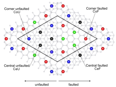
In principle, photoemission spectroscopy and STS provide direct access to the low-temperature electronic structure of surfaces. However, specific difficulties arise in the interpretation of the data in the case of Si(111)–77 that explain the conflicting results of the literature. The surface photovoltage (SPV) effectAlonso et al. (1990); Marsi et al. (1998) introduces in the low-temperature photoemission spectra an indeterminacy of the EF position of at least several tens of meV. This energy scale is critical for the Si(111)–77 surface and makes different datasets compatible with a metallicDemuth et al. (1983); Losio et al. (2000); Barke et al. (2006) or insulatingUhrberg et al. (1998) ground state. Low-temperature STS dataModesti et al. (2009); Odobescu and Zaitsev-Zotov (2012); Odobescu et al. (2015); Mysliveček et al. (2006); Wang et al. (2018) show the opening of a hard or soft gap below 20 K. However, the published STS spectra are integrated over the unit cell, or taken only on some kinds of the adatoms, or not suitably corrected for the systematic error caused by the non-equilibrium transport of carriers, which affects the energy scale at low temperaturesModesti et al. (2009); Mysliveček et al. (2006). Hence, these analyses do not allow us to identify the adatom-dependent effects of a gap opening at EF.
In order to clarify the low temperature state of the Si(111)–77 surface, we performed temperature-dependent photoemission and STS experiments. Thanks to our improved correction of the SPV the photoemission spectra clearly show that no band crosses the Fermi level at 17 K, thus excluding a metallic ground state. We also measured accurately corrected low-temperature tunneling spectra resolved on the four kinds of adatoms in the unit cell. Both photoemission and tunneling spectra consistently indicate a strong reduction of the spectral intensity near EF from RT to 17 K. Adatom-selective STS spectra show that this spectral intensity decrease also involves all the filled dangling bond states of one of the four kinds of adatoms. As a result, while at room temperature metallic surface states near EF are spread over all adatoms in the cell, a more inhomogeneous evolution takes place at low temperatures, where the weight of insulating states just below EF concentrates in three corner faulted adatoms closest to the vacancy site, surprisingly dropping in some of the others. We attempted to explain the observed insulating state by performing state-of-the-art DFT calculations in the generalized gradient approximation (GGA) of the structural and electronic properties of the Si(111)–77 surface. We allowed both the spin degree of freedom and the breaking of the C3v symmetry of the DAS model, and included strong electron correlation effects at the level of the DFT+U approximation. The calculations indicate that, while magnetic and non-magnetic phases, as well as undistorted or weakly Jahn-Teller distorted phases, are all nearly degenerate on this surface, no clear instability mechanism of the metallic state appears in this approximation. These results support the view that the actual mechanism that drives the insulating state and the massive spatial redistribution of spectral density at low temperature must be of non-mean field nature.
II Experimental and Computational Methods
The samples used for the STS measurements were heavily - (As-) doped Si(111) wafers with a resistivity of about 0.005 cm. The photoemission spectra were acquired at the VUV-Photoemission beamline of the Elettra synchrotron radiation source also from - (B-) doped (1-20 cm) and undoped (>2000 cm) samples. The surfaces were cleaned by flash heating up to 1600 K in ultra-high-vacuum (UHV) by electron bombardment and annealed at about 1100 K to obtain a well-ordered 77 reconstruction. The total energy resolution (photon + electron) of the photoemission spectra was 15 meV full width at half maximum (FWHM). The polarization of the synchrotron light was horizontal and laid in the scattering plane of the experiment, defined by the incoming photon beam and the axis of the cylindrical lens system of the electron analyzer. The sample temperature was estimated to be 173 K by replacing the sample with a Si-diode thermometer. The low-temperature spectra were corrected for the SPV shift Alonso et al. (1990); Marsi et al. (1998) within 15 meV as described in the Appendix A. The SPV effect also induces an energy broadening of the spectra due to the spatial inhomogeneity of the photon beam and the sample and the pulsed nature of the photon flux Marsi et al. (1998).
STS spectra and differential conductance (dI/dV) maps were measured far from defects on 77-reconstructed terraces with low surface defect densities (<0.5 1016 m-2, about 1 defect per 30 77 unit cells) by using a home-made STM with a gold tip. The STS spectra at 7 K have been corrected for the systematic errors caused by the transport of the charge carriers from the surface to the sample holder by using the method described in Ref. Modesti et al., 2009 with a tunneling current less than 1 pA between -0.5 and 0.5 V. This method allows the separation of the total bias voltage Vbias applied in STS in the potential drop across the tunnel junction between the tip and the surface region just below it, and the potential drop between this region and the sample holder. The surface and bulk carrier transport affects the latter potential drop, not the former. In this work the values of the voltage V used to compute and to plot the spectra at 7 K are, correctly, relative to the potential drop across the tunnel junction and not to the total drop between the tip and the sample holder Modesti et al. (2009). At 70 K and 295 K the STS spectra were measured with currents less than 1 pA and did not need the corrections mentioned above. The comparison between STS spectra acquired at different temperatures could be affected by accidental modifications of the tip and of its DOS during the temperature change. For this reason every STS spectrum reported in this article is the average of at least ten spectra obtained with different Au tips. We assume that the average electronic structure of the Au tips does not depend on temperature between 7 and 300 K. Under this assumption we consider the observed spectral changes as a function of T as due to variation of the electronic structure of the sample. At each temperature sets of STS spectra were acquired on the four different types of adatoms cyclically. Modifications of the tip structure were intentionally obtained by touching the Si surface between the acquisition cycles. As shown in appendix B on data reproducibility and data analysis, the characteristic spectral features of the different kinds of adatoms and the temperature dependence of the spectra do not depend on the tip properties. The maximum broadening in the dI/dV spectra due to numerical differentiation of I(V) is 0.01 V near the gap region.
Maps of the average dI/dV between -0.07 V and -0.20 V were obtained by acquiring I-V spectra on a 3232 spatial grid and computing the increment ratio of the current with respect to the bias voltage. The STS spectra and the conductance maps were acquired stabilizing the tip position at a bias voltage of 1.2 V or 1.4 V with a tunneling current of 3 pA or less. In this bias range the maximum spread of the apparent height of different adatoms in the STM topographic images is 0.15 Å. Taking into account the vertical position of the adatoms predicted by ab-initio calculations Smeu et al. (2012); Ke et al. (2000) the vertical tip-adatoms distance did change by less than 0.25 Å from one type of adatom to another.
First-principles DFT calculations were performed within the pseudopotential approximationBlöchl (1994) with the Vienna ab-initio Simulation package (VASP)Kresse and Furthmüller (1996a, b), in the GGA approximationPerdew et al. (1996). The Si(111)–77 surface was constructed according to the DAS model with C3v symmetry, with three Si bilayers to simulate the bulk-like substrate. The kinetic energy cutoff was set to 400 eV and the -point sampling of the Brillouin zone to a 55 Monkhorst-Pack uniform meshMonkhorst and Pack (1976). The bottom Si surface was saturated with hydrogens. Structural relaxation of the surface layer and of the topmost two Si bilayers was performed up to residual forces of 0.01 eV/Å. DOS and projected density of states (PDOS) were evaluated with -point mesh up to 1515 and electronic smearing of 0.01 eV.
III Results and analysis
III.1 DFT electronic structure - non-magnetic phase
Fig.2 shows the dispersion of the electronic bands close to EF calculated for a non-magnetic Si(111)–77 surface. We find 12 surface bands deriving from the 12 adatoms dangling bonds between -0.2 and 0.4 eV in the gap of the Si bulk states. The flat band at -0.45 eV arises mainly from the surface atom at the center of the hole. Projected bulk states are present below -0.5 eV.

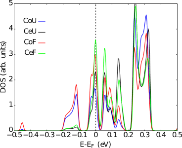
The surface is predicted to be metallic, as expected for a single-particle band picture, with two narrow bands crossing the Fermi level in the region between the center and the edges of the 77 surface Brillouin zone (SBZ), in agreement with the results of Ortega Ortega et al. (1998) In order to compare the DFT results with the experimental photoemission and dI/dV spectra the adatom PDOS and the local density of states (LDOS) 3 Å and 5 Å above the surface were computed for each kind of adatom. The calculated PDOS, presented in Fig. 2, confirms that the states close to EF are delocalized over all the adatoms in the surface unit cell. The PDOS at and below EF of the adatoms in the faulted part is higher than that of the adatoms in the unfaulted part. In each half, the central adatoms have a higher PDOS than the corner adatoms, in agreement with other computational resultsSmeu et al. (2012). As shown in Fig. 2 the PDOS has a relative maximum very close to EF on all the adatoms, related to an inflection point of the band dispersion at the point (see Fig. 2), and the values of the PDOS on inequivalent adatoms differ by less than a factor 2.5 in the first 0.1 eV below EF. Low energy states centered at -0.15 eV derive mainly from the corner adatoms. The small peak at about -0.45 eV is due to the interaction between the CoF adatoms and the atom at the center of the hole. The shapes and relative weights of the LDOS near EF calculated 3 Å and 5 Å above each adatom (not shown) do not depend on the distance from the surface and are similar to those of the PDOS within 20%, indicating that, in the Tersoff-Hamann approximation Tersoff and Hamann (1985), the experimental differential conductance on different adatoms (see below) can be interpreted, at least qualitatively, by means of the relative PDOS near EF.
III.2 Scanning tunneling spectroscopy
Fig. 3 shows the temperature dependence of dI/dV of the four types of adatoms of the 77 unit cell. All spectra at 7 K (lower panel of Fig. 3(a) and Fig. 3(b)) have energy gaps at EF of similar width (about 0.05 eV), indicating an insulating phase. This is in agreement with previous results obtained by averaging the spectra over all the adatomsModesti et al. (2009) or only some Odobescu and Zaitsev-Zotov (2012); Odobescu et al. (2015) of the adatoms in the unit cell, but contrasts with the calculated PDOS, which shows a maximum at EF. The two sets of data taken at 7 K on different samples with different tips show the degree of reproducibility of our tunneling spectra. The data noise in the region near the gap sets the upper limit of dI/dV at EF to 6% of the value measured at 295 K, the ratio RSTS of dI/dV at 7 K to that at 295 K at EF is 0.030.03. More details on the gap region of the tunneling spectra are reported in the second appendix. The spectra at 70 K show finite dI/dV values at EF for all the adatoms and increased spectral intensity for the CeU adatoms near the gap with respect to the 7 K case.
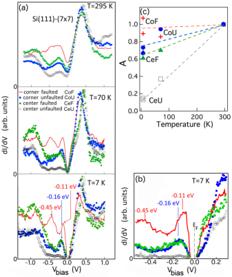
The data of Fig. 3 indicate a new aspect of the low-temperature electronic properties, namely the low dI/dV values on CeU adatoms in the first few hundreds mV below EF at 7 K, which are one order of magnitude lower than those of the other adatoms. The drop of the spectral intensity at low temperature is quantified in Fig. 3(c), which reports the mean value of the dI/dV between -0.07 and -0.20 V () normalized to its value at 295 K as a function of the temperature. decreases by more than a factor 6 from 295 to 7 K for the CeU adatoms, and by less than a factor 2 for the other adatoms. This adatom-specific behavior rules out spurious tip effects and highlights temperature-dependent changes of the electronic structure that affect the PDOS of the CeU adatoms near -0.2 eV or/and their tunneling probabilityFeenstra et al. (1987); Tersoff and Hamann (1985); not (b). Notably, DFT calculations of Section III.1 of the metallic, nonmagnetic and undistorted DAS surface do not explain the experimental observation, at least in the Tersoff-Hamann approximation.Tersoff and Hamann (1985) Adatom-resolved PDOS and LDOS differ by less than a factor 2.5 near EF, while dI/dV measured on the CeU adatoms is one order of magnitude smaller than on the other adatoms at 7 K.
In addition to the experimental insulating gap on all the adatoms, Fig. 3 shows well-defined peaks at 7 K between -0.11 V and -0.45 V, which correspond to features observed in the photoemission data of Refs. Uhrberg et al., 1998; Barke et al., 2006 and, therefore, can be associated to maxima of the surface DOS. The peak at -0.45 V on the CoF adatoms is also present in the calculated PDOS on the same adatom (see Fig. 2). It originates from the interaction with the dangling bond of the atom at the center of the hole. The peaks of the topmost filled states of the CeF and CoU adatoms, centered at -0.16 V, are slightly shifted with respect to that of the CoF adatom at 0.11 V (see Fig. 3(b)). The other peaks, already reported in previous studies at higher temperatures Mysliveček et al. (2006); Wolkow and Avouris (1988), are the maximum at -0.9 V, which is degenerate with the peak on the rest-atoms Brommer et al. (1993); Smeu et al. (2012); Wolkow and Avouris (1988), and the peak of the empty adatom states in the range of 0.2-0.4 V.
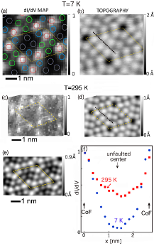
Fig. 4(a) shows the dI/dV map at 7 K averaged between -0.07 V and -0.20 V. This map confirms that the distribution of dI/dV related to the filled states close to the gap is strongly peaked on the CoF adatoms, while the regions of the CeU adatoms are empty, with a ratio equal to 25 between maxima and minima of the averaged dI/dV. This ratio decrease to 2 in the dI/dV map at 295 K (Fig. 4(c) and (e)), in line with the room temperature STS spectra of Fig. 3. These data support the distinct temperature dependence of the electronic properties of the CeU adatoms.
A map qualitatively similar to that of Fig. 4(a) is obtained at negative stabilization bias voltages. The main difference is a decrease of the contrast by approximately a factor 3 caused by the reduction of the tip-adatom distance in the unfaulted half of the unit cell necessary to compensate for the smaller PDOS of the occupied states. As shown in Fig. 3 the dI/dV signals differ by at most a factor 2 just above the gap, and are larger on the faulted half of the unit cell. Therefore, we expect that the dI/dV map of the empty states close to the gap displays a substantially smaller contrast, and again a minimum in the unfaulted part. This does not support a charge density wave picture of the ground state.
III.3 Angle-integrated photoemission
In order to verify the insulating state observed by the STS experiments, we performed a complementary investigation of the low-temperature electronic structure of Si(111)–77 by photoemission spectroscopy.
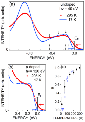
The angle-integrated photoemission spectra of Figs. 5(a) and 5(b), measured at 17 K and corrected for the SPV shift, show strongly reduced intensities at EF with respect to the 295 K data (horizontal arrows), providing a confirmation of the STS results. This drop can be quantified by the ratio R of the photoemission intensity at EF at a given temperature to that at 295 K, reported in Fig. 5(c) and compared with a similar ratio from the STS data. The differential conductance drops below the noise level at about 20 K, in agreement with Ref. Odobescu et al., 2015. At 17 K R from photoemission is 0.150.15, where the error is mainly caused by the propagation of the maximum error of the position of EF in the spectra, which reaches 15 meV at 17 K. The value 0.3 is the upper limit of the ratio between the DOS at EF at the two temperatures because the SPV-induced extrinsic broadening of the low-temperature spectra inflates the high-energy tail of the spectra at and above EF. The presence of dominant SPV broadening at 17 K is testified by the extent of the high-energy tail (more than 30 meV above EF), which is much larger than the experimental resolution (15 meV FWHM) and the thermal broadening of the Fermi distribution (6 meV). To obtain a more accurate estimate of the DOS at EF we took into account the SPV broadening by fitting the spectra at 17 K between -0.07 eV and 0.10 eV by the convolution of a Gaussian function, which describes the broadening, and the function , where is the energy and is the Fermi distribution at T=17 K. We approximated near EF by a linear function. One of the free parameters of the fit is the energy of the real Fermi level (that we call ) because of its 15 meV maximum error. The other three parameter are , the value of the linear function at normalized to its value at 295 K, the slope of the linear function, and the FWHM of the photovoltage broadening.
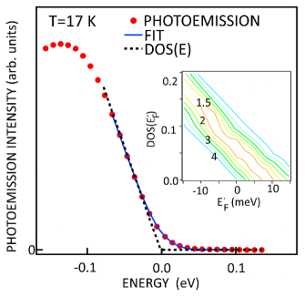
An example of the fit is shown in Fig. 6 for the case of and meV not (c), together with the (normalized to its minimum value), which measures the quality of the fit as a function of and . The best estimate for the at 17 K is . This range is determined by the condition and is a consequence of the weak dependence of the quality of the fit on . The FWHM of the SPV broadening is between 0.045 eV and 0.055 eV, confirming that it is considerably larger than the experimental energy resolution and the thermal broadening of the Fermi distribution at 17 K. The lower limits of both and the corresponding ratio obtained from the STS data (see Sect. III.2) are zero, consistent with the presence of an energy gap. The upper limit of is higher than that of (0.06) because of the propagation of the SPV-related error and the proximity of the temperature (20-30 K) at which the gap closes Modesti et al. (2009); Odobescu et al. (2015).
The observation of the dip at EF in the low-temperature photoemission data indicates that the deep minimum seen by STS is caused by a real drop of DOS and not mainly by a local Coulomb blockade, as suggested by Ref. Odobescu et al., 2015, or temperature-dependent tunneling probability effects, which do not affect the photoemission spectra. In addition, the energies of the adatom peaks observed in our STS spectra (indicated by dashed lines in Fig. 5(a)) agree with those of the peak at -0.14 eV and the shoulder at -0.45 eV of the photoemission spectrum, thus supporting the assigment of the STS features to maxima of the surface DOS. The spectra of undoped (Fig. 5(a)), -doped (Fig. 5(b) and Fig. 6) and -doped (Fig. 7(a), see below) samples present the same low-energy features within the experimental error, thus excluding observable effects of bulk doping, such as the modification of the population of the surface states and the contribution from bulk carriers to the photoemission spectra.
The two techniques, STS and angle-integrated photoemission, offer in conclusion a similar and coherent picture of a genuine gap-opening metal-insulator transition upon cooling. Alas, they do not explain why and how that transition, not predicted by DFT calculations, actually takes place.
III.4 Angle-resolved photoemission
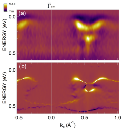
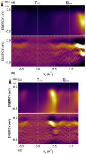
The nature of the low-energy states of this surface can be further investigated by measuring the dispersion of the adatom bands by angle-resolved photoemission spectroscopy (ARPES). Figure 7(a) reports spectra of the Fermi level region measured with 40 eV photons along the direction ( is the point of the unreconstructed 11 SBZ. The sequence of the 77 SBZ along this direction is sketched in Fig.7(b)). We observe three peaks at about -0.12, -0.29 and -0.45 eV, which match the peak and the shoulders of the angle integrated spectrum of Fig. 5(a). The general features of our spectra are in agreement with the photoemission data of Refs. Uhrberg et al., 1998; Barke et al., 2006, except for an energy shift caused by different treatments of the SPV effect. Our improved correction of the SPV and the high signal-to-noise ratio allow us to detect the three bands with low uncertainty in energy and in an extended momentum region (see Figs. 7(c)). The dispersions of these bands, marked by symbols in Figs. 7(d)–(f), are obtained by measuring the energies of the minima of the second derivative of the photoemission intensity with respect to the energy (Figs. 7(d)–(e)). These dispersions are confirmed by using the Laplacian and the curvature methods Zhang et al. (2011) and photon energies between 24 an 75 eV (see Appendix on data reproducibility and data analysis).
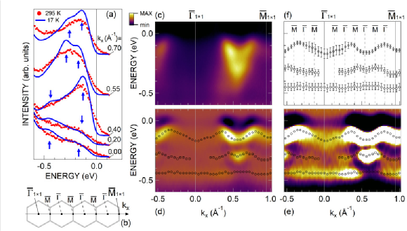
Fig. 8 show the sequence of the 77 SBZ along the direction of the 11 SBZ, the photoemission intensity map along this direction, and the band dispersions obtained by the second derivative method.
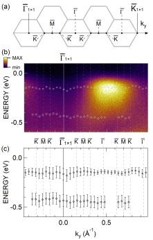
Figures 7 and 8 show that the band closest to EF, centered at -0.12 eV, never crosses the Fermi level along the and directions and stays at least 60 meV below EF, a binding energy which is more than four times the error of the position of EF. No other band closer to EF is observed for photon energies between 24 and 75 eV along high-symmetry directions. Additionally, we explored the electronic structure of the Si surface by ARPES over the whole 11 SBZ. The constant energy cuts of Fig. 9(a) and (b) show that the residual intensity at EF derives from the tails of features observed at deeper energies broadened by the SPV effect. We also display in Fig. 9(c–e) the energy-momentum maps taken along high-symmetry directions of the 77 SBZ marked by a thick cyan line in Fig. 9(a). In all these panels the photoemission peaks lie below EF.
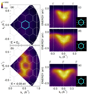
The low residual signal at EF visible at 17 K in Fig. 7(a) is due to the high-energy tail of the -0.12 eV band broadened by the SPV effect. Coherently, the lack of bands across EF and the binding energy larger than 60 meV of the topmost band are in agreement with the deep depression of the spectral intensity at EF observed in our STS and angle-integrated photoemission data. Moreover, our results are also consistent with the insulator-like photoemission data reported by Uhrberg et al. Uhrberg et al. (1998).
An intriguing feature of the band near EF is its dispersion. The energy of this band varies between about -0.08 eV and -0.15 eV along with alternating maxima and minima in the proximity of consecutive points of the repeated 77 BZ (see Figs. 7(d)-(f)). This behavior causes an apparent doubling of the period of the band dispersion with respect to the 77 period. The same band appears flat within our experimental error in the direction, which also contains and points. The anomalous period of the band dispersion, the interpretation of wich will require additional investigations, beyond the scope of the present work, could be related to the presence of four triplets of equivalent adatoms in the unit cell (see Fig. 1), which could give rise to modulation of the photoemission matrix elements in adjacent BZs by a structure factor term. An effect of this kind was observed for the first time in graphite Shirley et al. (1995), where the photoemission signals of the and states display strong intensity modulations in neighbouring BZs. The same effect in graphene causes a dispersion of the C 1s core level with a period different from that of the BZ Lizzit et al. (2010) and, in the iron-pnictide superconductor FeSexTe1-x, distinctive signatures of reciprocal lattice symmetry breaking in the ARPES spectrumMoreschini et al. (2014).
III.5 Magnetic phases
Motivated by the contrasting evidences from multiple experimental measurements and first-principles DFT results on the electronic properties of the Si(111)–77 surface, in particular by the presence of an energy gap, we extended our calculations to include possible symmetry breaking effects. We explored the possibility of a magnetic ground state, which could be the origin of a band insulating state with an odd number of electrons per unit cell, keeping the C3v point-group symmetry of the surface in the DAS model. Starting from the non-magnetic band structure in Fig. 2, the exchange splitting of a ferromagnetic surface should be at least 0.35 eV to shift the first minority adatom band high enough in energy to cause the complete filling of the five lowest majority adatom bands with the five adatom electrons and an energy gap at EF between the fifth majority band and the others. A smaller exchange splitting could still give rise to a magnetic insulator in the case of a breaking of the C3v symmetry that removes the degeneracy of the adatom bands at at 0.02 eV and 0.04 eV.
We tested this possibility allowing a spin polarization of the surface bands. The theoretical stability of a possible magnetic phase of this surface was not clearly solved in the literature, which contains conflicting resultsSheka et al. (2003); Solares et al. (2005). We performed a self-consistent calculation which starts from parallel non-zero magnetic moments on Si adatoms and converges to a ferromagnetic solution with a total magnetization of 2.3 per unit cell. The total energy of the magnetic solution, within our approximations, is about 0.5 meV/adatom lower than the non-magnetic solution, indicating nearly degenerate phases. The band structure of the ferromagnetic phase, reported in Fig. 10, shows an almost rigid shift between the majority and minority adatom bands with an exchange splitting of about 0.1 eV, which is less than the 0.35 eV necessary for an insulating state.

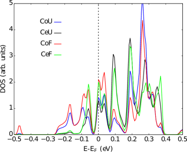
The band structure within 0.3 eV below EF has three (one) completely filled majority (minority) bands. Partially filled spin-up and -down bands eventually lead to a metallic ground-state, still in disagreement with the experiments. It is interesting, however, to calculate the effect of exchange splitting on the PDOS on the adatom sites, presented in Fig. 10, summing the majority and minority contribution in order to compare with non-spin-polarized STS results of Fig. 3. The DOS at EF is reduced by 30% with respect to the non-magnetic PDOS and the centroid of the occupied PDOS is shifted by about 50 meV towards higher binding energies with respect to the non-magnetic solution, thus partially improving the agreement with the experimental results. As evident from Fig. 10 the occupied manifold formed by four bands (three of majority spin and one of minority) is well separated from the bands at EF by an energy gap of 0.05 eV accommodating four of the five adatoms dangling bond electrons. The remaining electron is now responsible for the metallic nature of the surface because of the overlap of majority and minority bands at EF.
The magnetic moment of the surface is mainly localized on the adatoms of the faulted region, followed by the central adatoms of the unfaulted region and with a marginal contributions from corner adatoms of the unfaulted half. We also tested two other starting spin configurations including antiparallel guesses for the Si adatom spin polarizations. In particular, we considered a starting configuration in which the corner adatoms in the same (faulted or unfaulted) region are ferromagnetically aligned to each other while the two regions are antiferromagnetically coupled and the corresponding one for the central adatoms. In both cases the solution converges to the same metallic ferrimagnetic phase with a net magnetic moment of 1.0 and an energy about 1 meV/adatom lower than that of the non-magnetic case. The relative band structure is shown in Fig. 11. Interestingly, the system is half-metallic, showing a small insulating gap at EF in the majority spin channel, while remaining metallic in the minority one. That is because the exchange splitting, like in the ferromagnetic case, is not larger than 0.1 eV, not enough to avoid that EF intersects a manifold of bands degenerate at .

It is conceivable that a breaking of the C3v symmetry, caused by a structural or charge distortion that removes the degeneracy at , might induce an insulating state. That would represent a sort of band Jahn-Teller effect – either static or dynamic. For instance, in the case of the ferromagnetic solution, a structural distortion-induced splitting might separate the fourth majority adatom band from the others and move it below EF. In this way the system could have bands with integer occupation and become a magnetic insulator. We investigated if the inclusion of electronic correlation effects at the level of the DFT+U approximationLiechtenstein et al. (1995) can increase the exchange splitting near the Fermi level and/or stabilize a structural distortion that lowers the symmetry and make the surface insulating. We used a starting ferromagnetic configuration with random vertical displacements of the adatoms (with a maximum displacement of 0.2 Å). Structural relaxation in the DFT+U approximation, with the Hubbard repulsion term U set to a reasonable value of 2.0 eVProfeta and Tosatti (2007) and the exchange integral J set to 0.8 eV, fails to find an insulating state because the exchange splitting remains of the order of 0.1 eV near the Fermi level with no indication of a structural distortion. Indeed, the obtained band structure closely resembles the ferromagnetic solution shown in Fig. 10. This result does not in itself exclude some kind of correlation-assisted Jahn-Teller distortion. This type of possibility was met before, for example in , a narrow-gap Jahn Teller distorted insulator, Kiefl et al. (1992) which DFT+U calculations fail to describe, always stabilizing an undistorted metal.Capone et al. (2000). While we will return to this point in the discussion below, it is necessary to conclude here that no standard first-principles, mean-field approach we attempted succeeds to explain the experimental insulating state of Si(111)–77.
IV Discussion and Conclusions
Our complementary STS and photoemission data on the Si(111)–77 surface agree showing a strongly depleted or vanishing density of states at EF at and below 17 K, independently of bulk doping, and no surface band crossing the Fermi level. The binding energy of the band closest to EF measured by ARPES is larger than 60 meV, confirming the presence of an energy gap and a genuine insulating state. The small residual photoemission intensity at the nominal energy of the Fermi level in our 17 K spectra is explained by the 50 meV SPV-induced extrinsic broadening of the spectra, comparable to the binding energy of the topmost filled surface band. The proper treatment of SPV shift is crucial to resolve inconsistencies among previous photoemission studiesDemuth et al. (1983); Uhrberg et al. (1998); Losio et al. (2000); Barke et al. (2006), which report conflicting results. In addition, the differential conductance data presented in Section III.2 indicate that the electronic properties of the three CeU adatoms are appreciably more affected by the temperature than those of the other nine adatoms in the unit cell.
These experimental evidences are in contrast to the computational results of Section III.1 which predict a metallic surface with a peak of the DOS at EF and without relevant differences in the PDOS(EF) among the adatoms (not larger than a factor 2.5), in agreement with previous calculationsFujita et al. (1991); Ortega et al. (1998); Brommer et al. (1993); Smeu et al. (2012). This suggests that the proper description of the electronic properties of Si(111)– 77 surface should require additional ingredients with respect to the present calculations. A first step along this hypothesis was done performing a spin-polarized DFT calculation, finding different marginal magnetic instabilities of the surface which give rise to a finite magnetic moment. The band structure and density of states near the Fermi energy of the computed ferromagnetic and ferrimagnetic solutions are modified with an average shift of the occupied adatom states to higher binding energies with respect to the nonmagnetic bands. However, the studied magnetic solutions remain metallic because overlapping adatom bands degenerate at are still partially filled, due to the small exchange splitting.
We have further explored the possibility of a larger exchange splitting and a structural symmetry breaking taking into account strong correlation effects, within DFT+U approximation, without finding indications of an insulating state or structural distortions. However, local distortions, if not intrinsic of the perfect surface, could be still triggered by a long range effect of surface defects or subsurface dopant impurities, which are not considered in the present model.
Other missing elements that could also explain discrepancies between DFT predictions and the experimental results are correlation effects beyond the DFT+U level and strong electron-phonon coupling. Electron correlation effects, caused by both intra- and inter-site Coulomb repulsion, are not properly described within our mean-field DFT and DFT+U calculations and could lead to a Mott-Hubbard insulator or Wigner-like 2D crystallization. The presence of significant electron correlations is indeed consistent with the short lifetimes of the electronic surface state studied by ultrafast spectroscopy Mauerer et al. (2006) and with the value of the screened on-site Coulomb interaction on the Si adatoms estimated to be 1 eV Ortega et al. (1998); Hansmann et al. (2013b), twice larger than the energy range of the dangling-bond states of the adatoms.
We note that to eventually employ a better theoretical approach than DFT+U, for example DFT+ dynamic mean field theory (DMFT) Anisimov et al. (1997), a calculation presently impossible for Si(111)–77 because of its inordinate size, one should begin with the ferrimagnetic starting point. Antiferromagnetic spin waves gives rise to stronger quantum fluctuations than ferromagnetic ones, and a distortion-induced gap may ensue to stabilize the system.
On the other hand, electron-phonon interaction might lead, especially in conjunction with carrier localization, to some form of electron self-trapping Toyozawa (1961); Toyozawa and Shinozuka (472). In simple words, the electron’s negative charge may distort the ion lattice around itself, so much to give rise to a localized attractive potential that binds and traps the electron itself, giving rise to a self-trapped polaron with large effective mass, further enhancing electron correlations. The electron-phonon coupling constant measured by Barke et al. Barke et al. (2006) is 1, which could be large enough to induce such effects. Although speculative, this tentative scenario could nonetheless explain our observations as well as those of Refs. Persson and Demuth, 1984; Schillinger et al., 2005; D’angelo et al., 2009. This scenario appears to be supported by the STS temperature dependence. Specifically, the filled electronic states nearest to the EF, which in the high temperature metallic state are relatively evenly spread over all the unit cell adatoms, localize mostly onto the three near-vacancy corner faulted CoF adatoms in the low-temperature insulating state. Experimentally, recent applications of non-contact pendulum-AFM spectroscopy, Stipe et al. (2001) an ultra-sensitive technique that can detect and map surface electronic excitations and their changes, suggest that more precise information on the nature of this metal-insulator transition should be derived, similar to those obtained for the normal-superconductor transition Kisiel et al. (2011) or the valence changes of surface oxygen vacancies in SrTiO3 Kisiel et al. (2018).
In summary, our experimental and theoretical results call for a critical revision of the low-temperature electronic properties of the Si(111)–77 surface, which is not merely a standard test sample, but poses difficult problems undergoing interesting phenomena and instabilities, still in need to be further clarified.
Acknowledgements.
We are grateful to G. Giovannetti, A. Baraldi and M. Fabrizio for discussions. P. M., P. M. S., and C. C. acknowledge the “Progetto Premiale, Materiali e Dispositivi Magnetici e Superconduttivi per Sensoristica e ICT” and the project EUROFEL-ROADMAP ESFRI of the Italian Ministry of Education, University and Research (MIUR). E. T. acknowledges partial support by European Research Council Advanced Grant N. 834402 ULTRADISS, and by the Italian Ministry of University and Research through PRIN UTFROM N. 20178PZCB5. G. P. acknowledges support from CINECA Supercomputing Center through the ISCRA project and financial support from the Italian Ministry for Research and Education through the PRIN-2017 project “Tuning and understanding Quantum phases in 2D materials - Quantum 2D (IT-MIUR Grant No. 2017Z8TS5B)*
Appendix A Surface photovoltage correction
The photoemission spectra of semiconductor surfaces are affected by energy shifts and broadening caused by the SPV effect Alonso et al. (1990); Marsi et al. (1998) and by the charge carrier transport between the sample holder and the surface hit by the photons, which induce an uncertainty in the position of the Fermi level in the spectra.
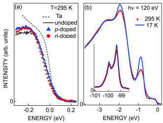
Its location and maximum error at 295 K in our data were determined by comparing the spectra taken on 77 surfaces of -, -doped and undoped samples, and on an Ag film deposited on Si and surrounded by the clean 77 surface, with the spectrum of a Ta plate on the sample holder (see Fig. 12(a)). The opposite SPV shifts of the spectra of -doped and -doped samples cause a maximum difference of 15 meV between the positions of high-energy cutoffs of the spectra, in agreement with Ref. Barke et al., 2006, which corresponds to a maximum error of ±8 meV in the position of EF at 295 K. To determine the SPV and carrier-transport shift at 17 K we measured the shifts of the Si 2p core level peaks, of the restatoms peak at -0.9 eV, and of the sharp features of the Si valence band cooling from 295 K to 17 K while keeping a constant photon flux at 120 eV. These shifts are the same within the experimental maximum error of ±5 meV for the Si 2p core levels and the -0.9 eV peak, and of ±20 meV for the valence band features. Fig. 12(b) shows that a rigid shift of -414 meV of the 17 K spectrum minimizes the differences between this spectrum and the RT spectrum both in the core level and in the valence band region in a -doped sample.
Therefore, we assume that the best estimate of the additional SPV shift in our low-temperature spectra is given by the rigid shift measured using the above-mentioned features at constant photon flux, while we use the shift of the valence band and of the -0.9 eV peak for photon energies lower than 120 eV. An additional source of error is a possible random shift less than 3 meV of the photon energy during the spectra acquisition. We estimate that the maximum error of the position of EF at 17 K is thus 15 meV by adding the error of the SPV at 295 K, that of the rigid shift from room to low temperature, and the energy stability of the photon beam.
*
Appendix B Data reproducibility, data analysis, and effects of defects
The variability of the tunneling spectra acquired with different Au tips on the CoF and CeU adatoms is shown in Figs. 13 and 14 for 295 K and 7 K respectively. Spectra of the two adatoms plotted with the same symbol in Fig. 13 or tagged with the same number in Fig. 14 were acquired with the same tip at the same time.
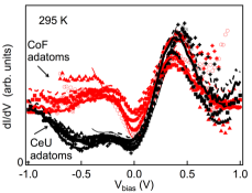
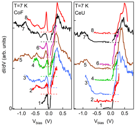
Each pair of spectra was taken with a different tip. Spectra obtained with insulating or semi-insulating tips (with low intensity near EF) are not reported and were not used for the analysis. The difference in the spectral intensity between -0.2 and 0.0 V between CoF and CeU adatoms is always observed, and reaches a factor of at least ten in all the cases at 7 K.
The peaks at -0.10 V and -0.45 V are always observed on the CeU adatoms at low temperature. The differences between the spectra obtained with different tips are mainly in the relative intensities of the parts at positive and negative voltages and in the intensity of the background at high bias voltages.
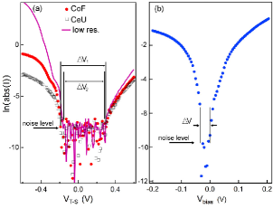
Fig. 15(a) shows the logarithm of the tunneling current as a function of the voltage bias between the sample holder and the tip (VT-S) measured on the CoF and CeU adatoms at high and low tunneling resistance. The voltage gap V2 in the low tunneling resistance curve is mainly caused by the transport of charge carriers between the surface below the tip and the sample holder and includes possible Coulomb blockade effects. The difference between the similar gap V1 in high resistance curves and V2 is the surface gap [21]. The same gap V is also visible when the logarithm of the current is plotted vs the voltage bias between the tip and the surface (Fig. 15(b)).
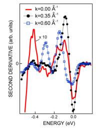
The analysis of the ARPES data of Fig. 7(c) with the Laplacian method or with the curvature method, show in Fig. 16, provides the same dispersion of the surface bands obtained with the second derivative with respect to energy reported in Fig. 7 within the experimental error. The increased noise level in these plots derives mainly from the derivative with respect to the wavevector k. The energy of the topmost band near of the 11 SBZ is reported with a large error in Fig. 7(d) and (f) because the maximum of the negative of the second derivative with respect to the energy is particularly broad for this wave vector, as shown in Fig. 17. The width of the peak of the second derivative at k=0 Å -1 is about twice those at larger wave vectors. A possible interpretation is the presence of two components, one at about -0.08 eV and the other at -0.14 eV. These two components and the structure factor mechanism mentioned in section III.4 are a possible explanation for the anomalous dispersion of the topmost band. Fig. 18, which reports the ARPES intensity plots and their second derivative for photon energies of 60 and 75 eV, shows that no new band at EF shows up at other photon energies.
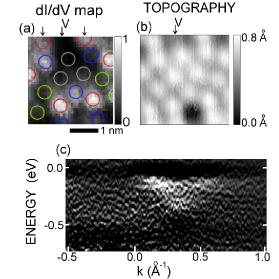
Missing adatoms in the center region of the unit cell are the dominant defects found on our well ordered Si(111)–77 surfaces. The effect of such vacancies on the electronic structure is shown in Fig. 19 which reports the map of the differential conductance between -0.1 V and -0.2 V on the left, and the topographic image of the same area containing a vacancy on the right. The dI/dV signal - approximately proportional to the integrated LDOS between -0.1 and -0.2 eV- is normalized to its maximum value. The signal on the FCo adatoms that are first nearest neighbors of the vacancy (red circles indicated by the left and right arrows) is about half of the signal on the FCo adatoms far from the defect (other red circles). Moreover the signal on the vacancy is substantially less than that of the relative adatom. Therefore a single vacancy substantially decreases the LDOS near EF on at least three sites. Coherently with this finding the photoemissions spectra show that the intensity of the peak at -0.12 eV is the most dependent on the sample preparation and that it reaches the highest intensity only on the cleanest samples after a proper annealing at 1100 K. The ARPES intensity plot in Fig. 19(c), measured in a sample with defect density so high that the -0.12 eV peak was attenuated by a factor two, shows that the gap and the band dispersion are not strongly affected by the defect density in comparison with Fig. 7 (d). The noise in the plot is caused by the short acquisition time used.
References
- Tosatti and Anderson (1974) E. Tosatti and P. W. Anderson, Jpn. J. Appl. Phys. 13, 381 (1974).
- Tosatti (1975) E. Tosatti, Festkorperprobleme 15, 113 (1975).
- Santoro et al. (1999) G. Santoro, S. Scandolo, and E. Tosatti, Phys. Rev.B 59, 1891 (1999).
- Carpinelli et al. (1996) J. M. Carpinelli, H. H. Weitering, E. W. Plummer, and R. Stumpf, Nature (London) 381, 398 (1996).
- Carpinelli et al. (1997) J. M. Carpinelli, H. H. Weitering, M. Bartkowiak, R. Stumpf, and W. E. Plummer, Phys. Rev. Lett. 79, 2859 (1997).
- Weitering et al. (1997) H. H. Weitering, X. Shi, P. D. Johnson, J. Chen, N. J. DiNardo, and K. Kempa, Phys. Rev. Lett. 78, 1331 (1997).
- Ramachandran and Feenstra (1999) V. Ramachandran and M. R. Feenstra, Phys. Rev. Lett. 82, 1000 (1999).
- Avila et al. (1999) J. Avila, A. Mascaraque, E. G. Michel, M. C. Asensio, G. LeLay, J. Ortega, R. Pérez, and F. Flores, Phys. Rev. Lett. 82, 442 (1999).
- Modesti et al. (2007) S. Modesti, L. Petaccia, G. Ceballos, I. Vobornik, G. Panaccione, G. Rossi, L. Ottaviano, R. Larciprete, S. Lizzit, and A. Goldoni, Phys. Rev. Lett. 98, 126401 (2007).
- Profeta and Tosatti (2007) G. Profeta and E. Tosatti, Phys. Rev. Lett. 98, 86401 (2007).
- Cortés et al. (2013) R. Cortés, A. Tejeda, J. Lobo-Checa, C. Didiot, B. Kierren, D. Malterre, J. Merino, F. Flores, E. G. Michel, and A. Mascaraque, Phys. Rev. B 88, 125113 (2013).
- Hansmann et al. (2013a) P. Hansmann, T. Ayral, L. Vaugier, P. Werner, and S. Biermann, Phys. Rev. Lett. 110, 166401 (2013a).
- Li et al. (2013) G. Li, P. Höpfner, J. Schäfer, C. Blumenstein, S. Meyer, A. Bostwick, E. Rotenberg, R. Claessen, and W. Hanke, Nat. Commun 4, 1620 (2013).
- Ming et al. (2017) F. Ming, S. Johnston, D. Mulugeta, T. S. Smith, P. Vilmercati, G. Lee, T. A. Maier, P. C. Snijders, and H. H. Weitering, Phys. Rev. Lett. 119, 266802 (2017).
- Wu et al. (2019) X. Wu, F. Ming, T. S. Smith, G. Liu, F. Ye, K. Wang, S. Johnston, and H. H. Weitering, arXiv e-prints , arXiv:1912.03242 (2019), arXiv:1912.03242 [cond-mat.supr-con] .
- Demuth et al. (1983) J. E. Demuth, B. N. J. Persson, and A. J. Schell-Sorokin, Phys. Rev. Lett. 51, 2214 (1983).
- Uhrberg et al. (1998) R. I. G. Uhrberg, T. Kaurila, and Y. C. Chao, Phys. Rev. B 58, R1730 (1998).
- Losio et al. (2000) R. Losio, K. N. Altmann, and F. J. Himpsel, Phys. Rev. B 61, 10845 (2000).
- Schillinger et al. (2005) R. Schillinger, C. Bromberger, H. J. Jänsch, H. Kleine, O. Kühlert, C. Weindel, and D. Fick, Phys. Rev. B 72, 115314 (2005).
- Barke et al. (2006) I. Barke, F. Zheng, A. R. Konicek, R. C. Hatch, and F. J. Himpsel, Phys. Rev. Lett. 96, 216801 (2006).
- Modesti et al. (2009) S. Modesti, H. Gutzmann, J. Wiebe, and R. Wiesendanger, Phys. Rev. B 80, 125326 (2009).
- Odobescu et al. (2015) A. B. Odobescu, A. A. Maizlakh, and S. V. Zaitsev-Zotov, Phys. Rev. B 92, 165313 (2015).
- Ortega et al. (1998) J. Ortega, F. Flores, and A. L. Yeyati, Phys. Rev. B 58, 4584 (1998).
- Tanikawa et al. (2003) T. Tanikawa, K. Yoo, I. Matsuda, S. Hasegawa, and Y. Hasegawa, Phys. Rev. B 68, 113303 (2003).
- Takayanagi et al. (1985) K. Takayanagi, Y. Tanishiro, M. Takahashi, and S. Takahashi, J. Vac. Sci. Technol. A 3, 1502 (1985).
- not (a) (a), a different model for this surface has been suggested by J. E. Demuth, arXiv:1905.12416 [cond-mat.mtrl-sci].
- Fujita et al. (1991) M. Fujita, H. Nagayoshi, and A. Yoshimori, Surf. Sci 242, 229 (1991).
- Brommer et al. (1993) K. D. Brommer, B. E. Larson, M. Needels, and J. D. Joannopoulos, Jpn. J. Appl. Phys 32, 1360 (1993).
- Smeu et al. (2012) M. Smeu, H. Guo, W. Ji, and R. A. Wolkow, Phys. Rev. B 85, 195315 (2012).
- Mårtensson et al. (1987) P. Mårtensson, W.-X. Ni, G. V. Hansson, J. M. Nicholls, and B. Reihl, Phys. Rev. B 36, 5974 (1987).
- Mysliveček et al. (2006) J. Mysliveček, A. Stróżecka, J. Steffl, P. Sobotík, I. Ošt’ádal, and B. Voigtländer, Phys. Rev. B 73, 161302 (2006).
- Odobescu and Zaitsev-Zotov (2012) A. B. Odobescu and S. V. Zaitsev-Zotov, J. Phys.: Condens. Matter 24, 395003 (2012).
- Efros and Shklovskii (1975) A. L. Efros and B. I. Shklovskii, Journal of Physics C: Solid State Physics 8, L49 (1975).
- Shklovskii and Efros (1994) B. I. Shklovskii and A. L. Efros, Electronic properties of Doped Semiconductors (Springer, Berlin, 1994).
- Persson and Demuth (1984) B. N. J. Persson and E. J. Demuth, Phys. Rev. B 30, 5968 (1984).
- Fick et al. (2006) D. Fick, C. Bromberger, H. J. Jänsch, O. Kühlert, R. Schillinger, and C. Weindelt, Surf. Sci. 600, 3835 (2006).
- Wells et al. (2006) J. W. Wells, J. F. Kallehauge, T. M. Hansen, and P. Hofmann, Phys. Rev. Lett. 97, 206803 (2006).
- D’angelo et al. (2009) M. D’angelo, K. Takase, N. Miyata, T. Hirahara, S. Hasegawa, A. Nishide, M. Ogawa, and I. Matsuda, Phys. Rev. B 79, 035318 (2009).
- Martins et al. (2014) B. V. C. Martins, M. Smeu, L. Livadaru, H. Guo, and R. A. Wolkow, Phys. Rev. Lett. 112, 246802 (2014).
- Just et al. (2015) S. Just, M. Blab, S. Korte, V. Cherepanov, H. Soltner, and B. Voigtländer, Phys. Rev. Lett. 115, 066801 (2015).
- Hansmann et al. (2013b) P. Hansmann, L. Vaugier, H. Jiang, and S. Biermann, J. of Phys.: Condens. Matter 25, 094005 (2013b).
- Pérez et al. (2001) R. Pérez, J. Ortega, and F. Flores, Phys. Rev. Lett. 86, 4891 (2001).
- Sheka et al. (2003) E. F. Sheka, E. A. Nikitina, and V. A. Zayets, Surf. Sci. 532-535, 754 (2003).
- Solares et al. (2005) S. D. Solares, S. Dasgupta, P. A. Schultz, Y.-H. Kim, C. B. Musgrave, and W. A. Goddard, Langmuir, Langmuir 21, 12404 (2005).
- Alonso et al. (1990) M. Alonso, R. Cimino, and K. Horn, Phys. Rev. Lett. 64, 1947 (1990).
- Marsi et al. (1998) M. Marsi, L. Nahon, M. E. Couprie, D. Garzella, T. Hara, R. Bakker, M. Billardon, A. Delboulbé, G. Indlekofer, and A. Taleb-Ibrahimi, J. Electron. Spectrosc. 94, 149 (1998).
- Wang et al. (2018) J. Wang, L. Jin, H. Zhou, H. Fu, C. Song, S. Meng, and J. Zhang, Applied Physics Letters 113, 031604 (2018), https://doi.org/10.1063/1.5038954 .
- Ke et al. (2000) S. H. Ke, T. Uda, and K. Terakura, Phys. Rev. B 62, 15319 (2000).
- Blöchl (1994) P. E. Blöchl, Phys. Rev. B 50, 17953 (1994).
- Kresse and Furthmüller (1996a) G. Kresse and J. Furthmüller, Phys. Rev. B 54, 11169 (1996a).
- Kresse and Furthmüller (1996b) G. Kresse and J. Furthmüller, Computational Materials Science 6, 15 (1996b).
- Perdew et al. (1996) J. P. Perdew, K. Burke, and M. Ernzerhof, Phys. Rev. Lett. 77, 3865 (1996).
- Monkhorst and Pack (1976) H. J. Monkhorst and J. D. Pack, Phys. Rev. B 13, 5188 (1976).
- Tersoff and Hamann (1985) J. Tersoff and D. R. Hamann, Phys. Rev. B 31, 805 (1985).
- Feenstra et al. (1987) R. M. Feenstra, J. A. Stroscio, and A. P. Fein, Surf. Sci 181, 295 (1987).
- not (b) (b), assuming a constant DOS of the tip, the differential conductance at a given bias voltage(Vbias) is approximately proportional to the surface PDOS(eVbias), multiplied by the tunneling probability, plus a background term proportional to a weighted average of PDOS(eV) from 0 to eVbias Feenstra et al. (1987). Therefore, the drastic decrease of dI/dV at about -0.2 V on the CeU adatom from 295 to 7 K derives by a comparable reduction of its PDOS(E) between 0.0 eV and -0.2 eV or/and by a drop of the tunneling probability, which is related to the sample wavefunctions in the vacuum regionFeenstra et al. (1987); Tersoff and Hamann (1985). In both cases the drop of dI/dV points to a significant temperature dependent modification of the electronic structure on the CeU adatoms near EF.
- Wolkow and Avouris (1988) R. Wolkow and P. Avouris, Phys. Rev. Lett. 60, 1049 (1988).
- not (c) (c), the value of E’F is referred to the best estimate of EF.
- Zhang et al. (2011) P. Zhang, P. Richard, T. Qian, Y. M. Xu, X. Dai, and V. Ding, Rev. Sci. Instrum. 82, 043712 (2011).
- Shirley et al. (1995) L. E. Shirley, L. J. Terminello, A. Santoni, and F. J. Himpsel, Phys. Rev. B 51, 13614 (1995).
- Lizzit et al. (2010) S. Lizzit, G. Zampieri, L. Petaccia, R. Larciprete, P. Lacovig, E. D. L. Rienks, G. Bihlmayer, A. Baraldi, and P. Hofmann, Nature Phys 6, 345 (2010).
- Moreschini et al. (2014) L. Moreschini, P.-H. Lin, C.-H. Lin, W. Ku, D. Innocenti, Y. J. Chang, A. L. Walter, K. S. Kim, V. Brouet, K.-W. Yeh, M.-K. Wu, E. Rotenberg, A. Bostwick, and M. Grioni, Phys. Rev. Lett. 112, 087602 (2014).
- Liechtenstein et al. (1995) A. I. Liechtenstein, V. I. Anisimov, and J. Zaanen, Phys. Rev. B 52, R5467 (1995).
- Kiefl et al. (1992) R. F. Kiefl, T. L. Duty, J. W. Schneider, A. MacFarlane, K. Chow, J. Elzey, P. Mendels, G. D. Morris, J. H. Brewer, E. J. Ansaldo, C. Niedermayer, D. R. Noakes, C. E. Stronach, B. Hitti, and J. E. Fischer, Phys. Rev. Lett. 69, 2005 (1992).
- Capone et al. (2000) M. Capone, M. Fabrizio, P. Giannozzi, and E. Tosatti, Phys. Rev. B 62, 7619 (2000).
- Mauerer et al. (2006) M. Mauerer, I. L. Shumay, W. Berthold, and U. Höfer, Phys. Rev. B 73, 245305 (2006).
- Anisimov et al. (1997) V. I. Anisimov, A. I. Poteryaev, M. A. Korotin, A. O. Anokhin, and G. Kotliar, J. Phys. Cond. Matter 9, 7359 (1997).
- Toyozawa (1961) Y. Toyozawa, Prog. Theor. Phys 26, 29 (1961).
- Toyozawa and Shinozuka (472) Y. Toyozawa and Y. Shinozuka, Phys. Soc. Jpn. 48, 472 (472).
- Stipe et al. (2001) B. C. Stipe, H. J. Mamin, T. D. Stowe, T. W. Kenny, and D. Rugar, Phys. Rev. Lett. 87, 096801 (2001).
- Kisiel et al. (2011) M. Kisiel, E. Gnecco, U. Gysin, L. Marot, S. Rast, and E. Meyer, Nat. Mater. 10, 119 (2011).
- Kisiel et al. (2018) M. Kisiel, O. O. Brovko, D. Yildiz, R. Pawlak, U. Gysin, E. Tosatti, and E. Meyer, Nat. Commun. 9, 2946 (2018).