First-principles calculations of defects in metal halide perovskites:
a performance comparison of density functionals
Abstract
Metal halide perovskite semiconductors have outstanding optoelectronic properties. Although these perovskites are defect-tolerant electronically, defects hamper their long-term stability and cause degradation. Density functional theory (DFT) calculations are an important tool to unravel the microscopic structures of defects, but results suffer from the different approximations used in the DFT functionals. In the case of metal halide perovskites, qualitatively different results have been reported with different functionals, either predicting vacancy or interstitial point defects to be most dominant. Here, we conduct a comprehensive comparison of a wide range of functionals for calculating the equilibrium defect formation energies and concentrations of point defects in the archetype metal halide perovskite, MAPbI3. We find that it is essential to include long-range Van der Waals interactions in the functional, and that it is vital to self-consistently optimize structure and volume of all compounds involved in the defect formation. For calculating equilibrium formation energies of point defects in MAPbI3 and similar metal halide perovskites, we argue that the exact values of the chemical potentials of the species involved, or of the intrinsic Fermi level, are not important. In contrast to the simple Schottky or Frenkel pictures, we find that the dominant defects are MA and I interstitials, and Pb vacancies.
I Introduction
Metal halide perovskites are emerging photovoltaic materials for solar cells, whose power conversion efficiency (PCE) has increased spectacularly from a few to over 25 percent over the last decade [1, 2]. The impressive photovoltaic performance is linked to the materials’ defect tolerance [3, 4], and attributed to a low intrinsic defect density, - cm-3, [5, 6, 7, 8, 9, 10] and to the dominant defects not creating deep trap levels [11, 12]. Despite the impressive progress, the long-term stability of the perovskite solar cells is still limited, which is ascribed to intrinsic instabilities of the material, and to defect-triggered degradation reactions [13, 14, 15, 4, 16, 17, 18, 19, 20, 21].
The defects in halide perovskites are rich in types and charge states. Taking the prime metal halide compound MAPbI3 as an example, there are already six different simple point defects, i.e. vacancies and interstitials, and this number is doubled or tripled if one takes different charge states into consideration [11]. To increase the long-term efficiency and stability of perovskite solar cells, it is necessary to come up with efficient strategies for defect passivation, which requires an understanding of the fundamental defect chemistry and physics of perovskites. It is therefore essential to identify the types and densities of defects, and their consequences for the electronic properties.
In experiment, the overall density and distribution of trap states can be extracted through electrical measurements [10, 6, 5]. However, it remains challenging to pin-point the exact types of defects and correlate those to electronic trap states [22]. Another challenge emerging from experiments is that the types of dominant defects can depend on details of the fabrication process, such as the ratio of precursor materials used [11, 23, 24], or the thermal annealing procedure [14, 25, 26], leading to different morphology and final compositions. This stresses the importance of being able to identify which defects would be present under ideal thermodynamic conditions.
To provide atomistic insight in the defect physics, computational modelling based upon density functional theory (DFT) is often invoked. In particular, one focuses on calculating the defect formation energies (DFEs) and charge state transition levels (CSTLs), which are key quantities for predicting the abundance and the electronic nature of defects [27]. Unfortunately, the quality of density functionals is not yet at a stage that all key defect quantities can be obtained simultaneously with the same accuracy [28]. Besides total energy differences between pristine and defective structures, obtaining DFEs requires accurate calculations of the thermochemistry (formation enthalpies) of sometimes widely different compounds (metals, insulators, molecules), as well as of basic electronic properties, such as band edge positions and band gaps.
A general-purpose semi-local functional based upon the generalized gradient approximation (GGA), such as the Perdew-Burke-Ernzerhof (PBE) functional [29], can lead to errors in formation enthalpies of order eV/atom [30, 31]. Hybrid functionals do not give a uniform improvement [30, 32], and in some cases, (transition) metals in particular, yield significantly worse formation enthalpies [33]. Given the fact that using a hybrid functional increases the computational costs by one to two orders of magnitude, and the results depend on how and how much Hartree-Fock exchange is mixed in, hybrid functionals seem a less attractive option for calculating formation enthalpies at present.
To deal with the imperfect formation energies resulting from PBE, semi-empirical schemes have been developed, such as the fitted elemental-phase reference energies (FERE) approach [34, 35]. It assumes the error predominantly depends on the overall composition, and attempts an improvement through using the total energies of elemental phases as fitting parameters. The FERE approach can improve DFEs significantly [35], but it requires the construction of an extensive parameter set for each group of compounds studied.
A significant step forward is presented by the recently developed strongly constrained and appropriately normed (SCAN) meta-generalized gradient approximation (meta-GGA) functional [36, 37]. Compared to standard GGA, SCAN more uniformly improves formation enthalpies of both strongly bonded solids and molecules [30, 32, 38], typically at least halving the error as compared to PBE [31].
A complicating factor in solids such as the hybrid metal-halide perovskites, is that heavy elements like Pb and I are involved, and organic cations are embedded in the inorganic metal-halide framework, both of which suggest that Van der Waals (vdW) interactions may play a non-negligible role in the bonding. The simplest way to include vdW interactions, is to add an atom-pairwise parametrized vdW energy to a standard DFT total-energy expression, such as in the D3 or D3(BJ) schemes [39, 40], leading to the PBE-D3 and PBE-D3(BJ) functionals, for instance. Mixed results have been reported, where PBE-D3/D3(BJ) gives good results on the cohesive energy of rare-gas solids, for instance [30], but PBE-D3 does not perform well in cases where anion-anion interactions play a significant role [38].
A fundamentally different approach constructs an explicitly non-local density functional, which incorporates vdW interactions directly, where one has to carefully balance these non-local with (semi-)local terms in the functional. The rev-vdW-DF2[41, 42, 43, 44] functional shows good results for weakly and strongly bound solids, with errors in formation energies on the scale of eV/atom, as does the SCAN+rVV10 functional, where the latter has the additional advantage that it is more accurate for molecules as well [45].
The functionals mentioned above do not solve the band gap problem of DFT [28, 35]. This problem is actually less severe if calculating DFEs under thermodynamic equilibrium conditions, as we will discuss below, which is the focus of the present paper. To calculate electronic properties such as CSTLs accurately on an absolute energy scale, requires the correct positions of the band edges. Post-processing DFT results using GW or hybrid functional calculations can in principle be applied for this purpose [35, 46], but in the present paper we will only compare pure DFT calculations.
Defect calculations on hybrid metal iodide perovskites using the PBE functional, have found the iodine vacancy to be one of the dominant point defects [47, 48, 49, 50]. In contrast, more recent studies incorporating vdW corrections using the DFT-D3 scheme, as well as a hybrid functional post-processing step, have led to the conclusion that the iodine interstitial is a more dominant point defect [51, 46, 52]. These studies illustrate the sensitivity of the predicted defect properties to the functionals used, and call for a careful and systematic comparison.
Whereas the addition of semi-empirical atom-pairwise vdW corrections within the D3 approach [39] have a sizable effect on the calculated DFEs of MAPbI3 [46], an improved version based on the same scheme with Becke and Johnson damping added (DFT-D3(BJ)) [40], which provides better corrections for non-bonding distances and intramolecular interactions [53], has not been tried yet. The same holds for accurate non-local vdW density functionals, such as rev-vdW-DF2.
The SCAN functional is reported to perform better than standard GGA functionals in predicting the orientation of organic cations in halide perovskites and the phase transitions of these materials [54, 55], but has not yet been applied in calculating defects of halide perovskites. The non-local correlation functional rVV10 seamlessly supplements SCAN with long-range vdW interactions [56], and the resulting SCAN+rVV10 functional [57] can also be tested in defect calculations on hybrid metal halide perovskites. Finally, as these perovskites contain heavy elements like Pb and I, the effects of spin-orbit coupling (SOC) should also be considered [58].
In the present work, we use a wide range of functionals to calculate the DFEs and CSTLs of the intrinsic vacancies and interstitials in MAPbI3, including PBE, PBE-SOC, SCAN, PBE-D3, PBE-D3(BJ), rev-vdW-DF2 and SCAN+rVV10. Comparing all data sets to the ones obtained by using PBE, the effects of switching from GGA to meta-GGA, from pairwise atomic to non-local vdW corrections, with and without SOC, are analyzed. While SOC has only little effect on the structures and the energies, it does impact the positions of the CSTLs. However, the latter can be straightforwardly included by applying an post-correction.
In contrast, the inclusion of vdW interactions is shown to have a large effect on the DFEs, where the PBE-D3(BJ), rev-vdW-DF2 and SCAN+rVV10 functionals give similar results. To obtain accurate results, we find that it is vital to optimize structures self-consistently for each functional. The SCAN functional captures part of the non-chemical bonding interactions, but including long-range vdW interactions, as in SCAN+rVV10, still has a sizable effect on the DFEs. Considering that it is a universally applicable functional for accurate calculations on solids and molecules, we suggest to use SCAN+rVV10 also for studying defects in other perovskite compounds.
II Computational Approach
II.1 DFT calculations
DFT calculations are performed with the Vienna ab initio simulation package (VASP) [59, 60, 61]. Defects are created starting from a 222 tetragonal supercell of the MAPbI3 perovskite structure with optimized volume and ionic positions. For each type of defect, cation or anion interstitial or vacancy, several different defective structures are tested, inserting or removing a cation or an anion in a different nonequivalent position, and optimizing the ionic positions within the supercell. The structures with the lowest total energy are then selected, and will be discussed below. A more detailed description of the strategy for creating the defective structures is given in the Supplemental Material, Figures S2-S4.
These calculations are repeated for the following functionals: PBE [29], SCAN [36], PBE-D3 [39], PBE-D3(BJ) [40], rev-vdW-DF2 [41, 42, 43, 44] and SCAN+rVV10 [57], using the default parameters appropriate for the respective functionals. To assess the influence of spin-orbit coupling, we have also tested PBE+SOC [58], as well as SCAN+SOC, but this time only on PBE- and SCAN-optimized structures, respectively. Our calculations use a plane wave kinetic energy cutoff of 500 eV and a -point only -point mesh. The energy and force convergence criteria are set to 10-4 eV and 0.02 eV/Å, respectively.
II.2 Defect formation energies
The defect formation energy (DFE) is calculated from
| (1) | ||||
Here indicates the type of defect, interstitial or vacancy, and is its charge. and are the DFT total energies of the defective supercell and the pristine supercell, respectively. As it only makes sense to compare total energies of systems with the same atomic and electronic contents, and this is clearly not the case comparing a defective with a pristine cell, one has to define reservoirs to make up for the surplus or shortage of atoms and electrons of the defective cell. Here, and define the number of atoms and the chemical potential of the species added to () or removed from () the pristine supercell in order to create the defective supercell.
Likewise, the Fermi level defines the electrochemical potential for electrons, if electrons need to be added or removed from the pristine supercell to create the charge . Ordinarily one chooses the zero of at the valence band maximum (VBM), so its energy appears in the expression of Eq. (1). The VBM is typically hard to identify in a calculation of a defective cell, so one uses the value obtained from the pristine cell, shifted by , which is, for instance, calculated by lining up the core level on one same atom in the pristine and the defective cell that is far removed from the defect.
Finally, is introduced to correct for the electrostatic interaction between a charged point defect and its periodically repeated images. In agreement with Ref. 46 we find that the 222 tetragonal supercell and the dielectric screening in MAPbI3 are in fact sufficiently large, such that this correction is small and can be neglected.
The chemical potentials of the atomic species depend upon the growth and environmental conditions, but they are subject to some constraints. The conditions must be such that the MAPbI3 phase is stable. In addition, we suppose it is in equilibrium with the PbI2 phase. Moreover, the MAI phase is not supposed to form. This leads to the following relations
| (2a) | |||
| (2b) | |||
| (2c) | |||
All chemical potentials used in this work are represented by DFT total energies of the compounds involved, see Supplemental Information Table S4. The combination of Eqs. (2a) and (2b) leaves one free parameter. Choosing , where is the energy of a I2 molecule, defines I-rich conditions. We have chosen this reference state to conform to previous calculations [51, 46, 52]. One may argue that the energy of a I2 molecule in a bulk iodine environment, , is a more appropriate reference state. However, as we will show below, the exact choice of the iodine reference state is not so important when studying defects under intrinsic conditions. Choosing , where is the energy of a Pb atom in bulk Pb metal, defines I-poor conditions.
The presence of molecule I2 (I-rich) or bulk Pb (I-poor) represent rather extreme conditions, neither of which are representative for the growth and environmental conditions of MAPbI3. We focus on so-called I-medium conditions, which are halfway between I-rich and I-poor, and thus defined by
| (3) |
The chemical potentials of Pb and MA can then be obtained from Eqs. (2b) and (2a), respectively, whereas the constraint of Eq. (2c) is then automatically obeyed.
Given the DFEs, the concentration of each type of defect can be estimated by Boltzmann statistics
| (4) |
where is the density of possible sites for the defect (see Supplemental Information Table S3), is the temperature, and is the Boltzmann constant. The concentration of charged defects () is obviously a function of the Fermi level , see Eqs. (1) and (4).
II.3 Intrinsic conditions
If no charges are injected in a material, it has to be charge neutral, as expressed by
| (5) |
where and are the intrinsic charge carrier densities of electrons and holes of the semiconductor material, and the sum is over all types of charged defects. Here , , and are functions of , so the charge neutrality condition, Eq. (5), serves to determine the intrinsic position of the Fermi level . Note that, if is sufficiently far from the band edges, then and are small, and can be neglected.
Under intrinsic conditions, defined by Eq. (5), the DFEs and concentrations of the most prominent defects turn actually to be independent of the iodine chemical potential over a large range of the latter [62]. If one changes to , then at a fixed Fermi level the DFE of an iodine interstitial changes from to , Eq. (1). Because of the equilibria of Eqs. (2b) and (2a), the DFEs of Pb and MA interstitials then change to and , respectively. Likewise, under the same conditions the DFEs of I, Pb, and MA vacancies charge to , , and , respectively.
Close to intrinsic conditions, point defects in MAPbI3 turn out to have a preference for a specific charge state, i.e., , , , , , . Following the discussion of the previous paragraph, if one changes the iodine chemical potential from to , the DFEs at a fixed Fermi level of these point defects change to , where is the charge of the defect. If one now applies the charge neutrality condition, Eq. (5), assuming that the Fermi level stays sufficiently far from the band edges such that , then the intrinsic Fermi level changes to .
This means that, according to Eq. (1), the change in intrinsic Fermi level compensates exactly for the change in iodine chemical potential for the DFEs of the mentioned point defects, and the DFEs remain unaltered. In other words, the DFEs and concentrations of these defects are independent of the iodine chemical potential.
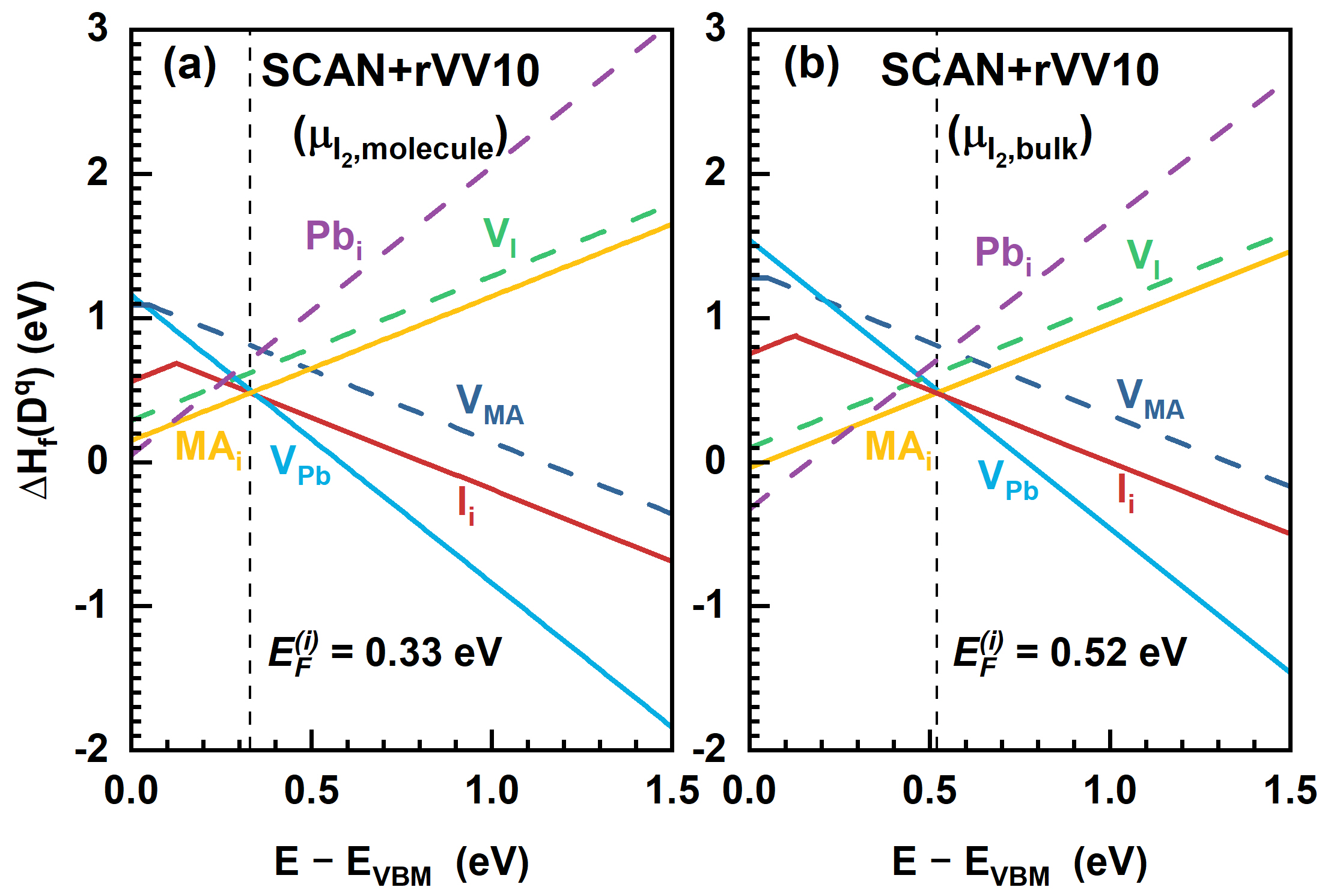
This effect is illustrated in Fig. 1, showing the DFEs calculated with the SCAN+rVV10 functional, using or , respectively in Eq. (3). Note that this does not mean that the DFEs of all charge states are unaltered. For instance, becomes (compare the upward sloping red lines in Fig. 1(a) and (b)). For MAPbI3 under normal equilibrium conditions, these particular charged states do not play a role, however.
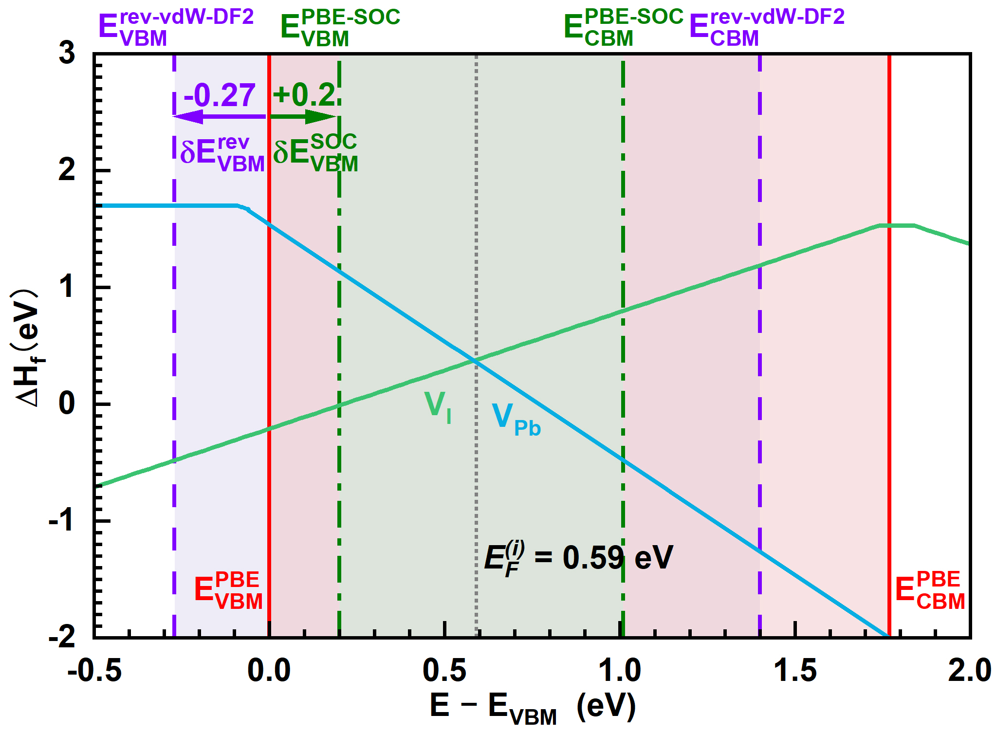
At intrinsic conditions, Eq. (5), the DFEs are also independent of the size of the band gap, or indeed of the exact positions of the band edges (VBM and CBM). To illustrate this, Fig. 2 shows the band edge positions calculated with the PBE-SOC and rev-vdW-DF2 functionals, relative to those calculated with the PBE functional, lining up the 1s core level of a carbon atom on a MA molecule. Because of the difference in VBM, the intrinsic Fermi level relative to the VBM, is different in all three cases. However, the DFEs at (calculated with the respective functional) are the same for all three functionals. This is the basis of a posteriori band edge corrections for defect calculations [35]. Of course, using a different functional for calculating the DFEs, the latter can still change, which will be discussed in Sec. III.
II.4 Charge state transition levels
Under non-equilibrium, operating, conditions, charges are injected in the material, shifting the position of the (quasi) Fermi level(s). The charge state transition level (CSTL) is defined as the Fermi level position where the charge states and of the same type of defect have equal formation energy, , so that if the Fermi level crosses the CSTL, the defect changes its charge state. As the DFEs have a simple linear dependence on , Eq. (1), this condition translates into
| (6) |
where is the defect formation energy calculated for . In calculating CSTLs, the absolute position of the VBM obviously plays a role.
III Results and discussion
III.1 PBE calculations
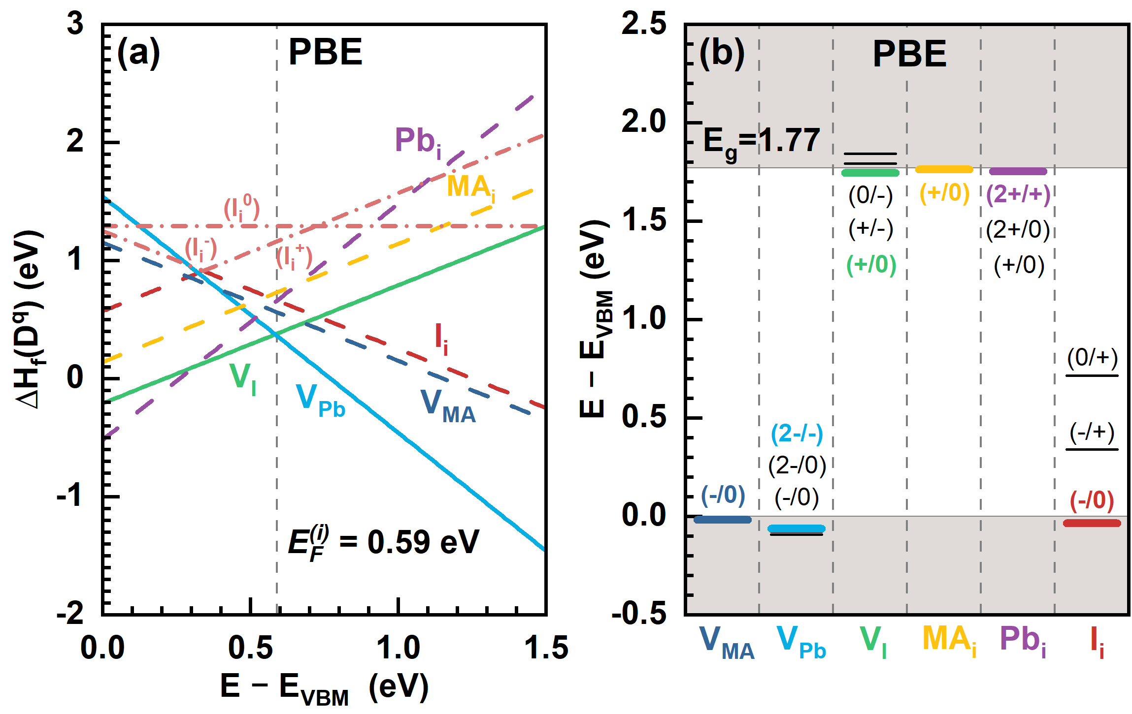
As PBE is the most widely employed functional, we will use it as reference for studying the defect thermodynamics and electronic properties. The calculated DFEs and CSTLs are shown in Fig. 3. At equilibrium conditions, as expressed by the charge neutrality condition, Eq. 5, the intrinsic Fermi level eV. At these conditions, the most stable point defects are the vacancies and with DFEs of 0.36 eV and 0.38 eV, respectively, which leads to equilibrium concentrations, Eq. 4, of and for these defects, respectively.
The formation energies of the other elementary point defects , , and , are 0.2 to 0.4 eV higher, resulting in a lower equilibrium concentration by a factor of to . PBE calculations thus support the classic picture of Schottky defects in ionic crystals, as represented by the oppositely charged vacancies and .
The CSTLs of these defects, calculated with the PBE functional, are shown in Fig. 3(b). One defect can have more than two charge states, and thus more than one transition level, where it is also possible that the charge changes by more than one unit . However, starting from one stable charge state of a defect, only the transition levels representing a change of a single unit are considered to be active. This is because the probability of capturing two or more holes/electrons simultaneously is very low [63, 46].
III.2 SOC, Van der Waals and meta-GGA functionals
Keeping the PBE results as a reference, we now turn to different functionals. The most obvious ingredients to add, are Van der Waals (vdW) interactions. The simplest approach uses parameterized semi-empirical expressions on top of the PBE functional, leading to the PBE-D3 or PBE-D3(BJ) functionals [39, 40]. An alternative approach defines explicit non-local terms representing vdW interactions. They can be incorporated in the density functional, as in the rev-vdW-DF2 functional, or added seamlessly to an existing functional, such as rVV10. Switching from a standard GGA to a more advanced meta-GGA functional, we also use the SCAN functional, without and with explicit vdW terms, the latter in the form of SCAN+rVV10. Spin-orbit coupling (SOC) can be added straightforwardly to the Hamiltonian, irrespective of the density functional.
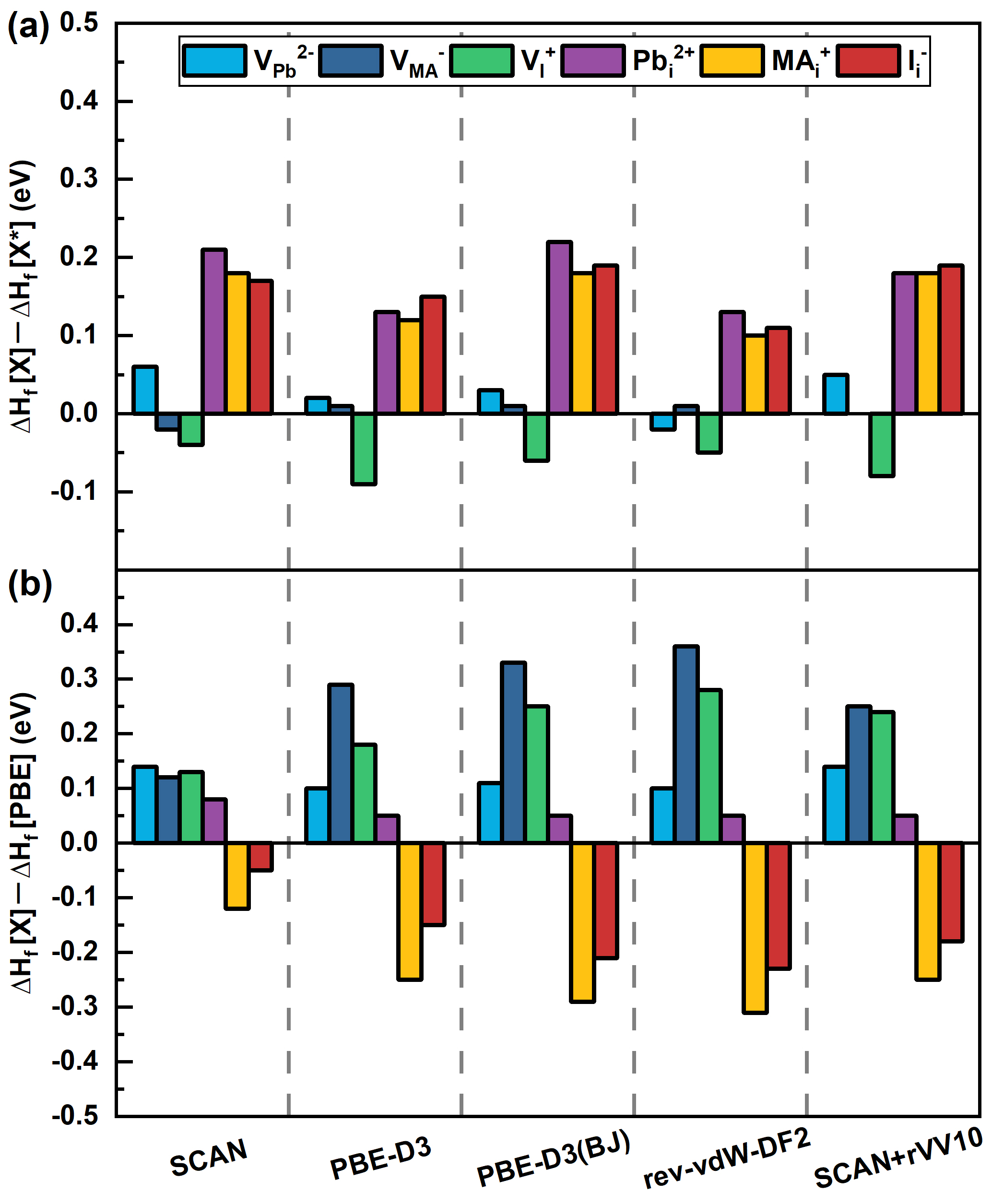
Previous defect studies on hybrid metal halide perovskites often adopt the strategy of applying vdW interactions, SOC, or hybrid functionals to the equilibrium structures optimized by PBE, in order to avoid the high computational costs associated with geometry optimization [65, 51, 46]. We perform two sets of calculations, a first set where the different functionals are used on the structures optimized by PBE, and a second set where all structures are optimized self-consistently with the respective functionals. This allows us to assess the effects on the DFEs of replacing the functional, and of geometry optimization separately. The results of the first set of calculations are discussed in this section, and those of the second set in the next section. The changes in the calculated DFEs if switching from the PBE functional to one of the other functionals (while keeping the geometries fixed), are shown in Fig. 4.
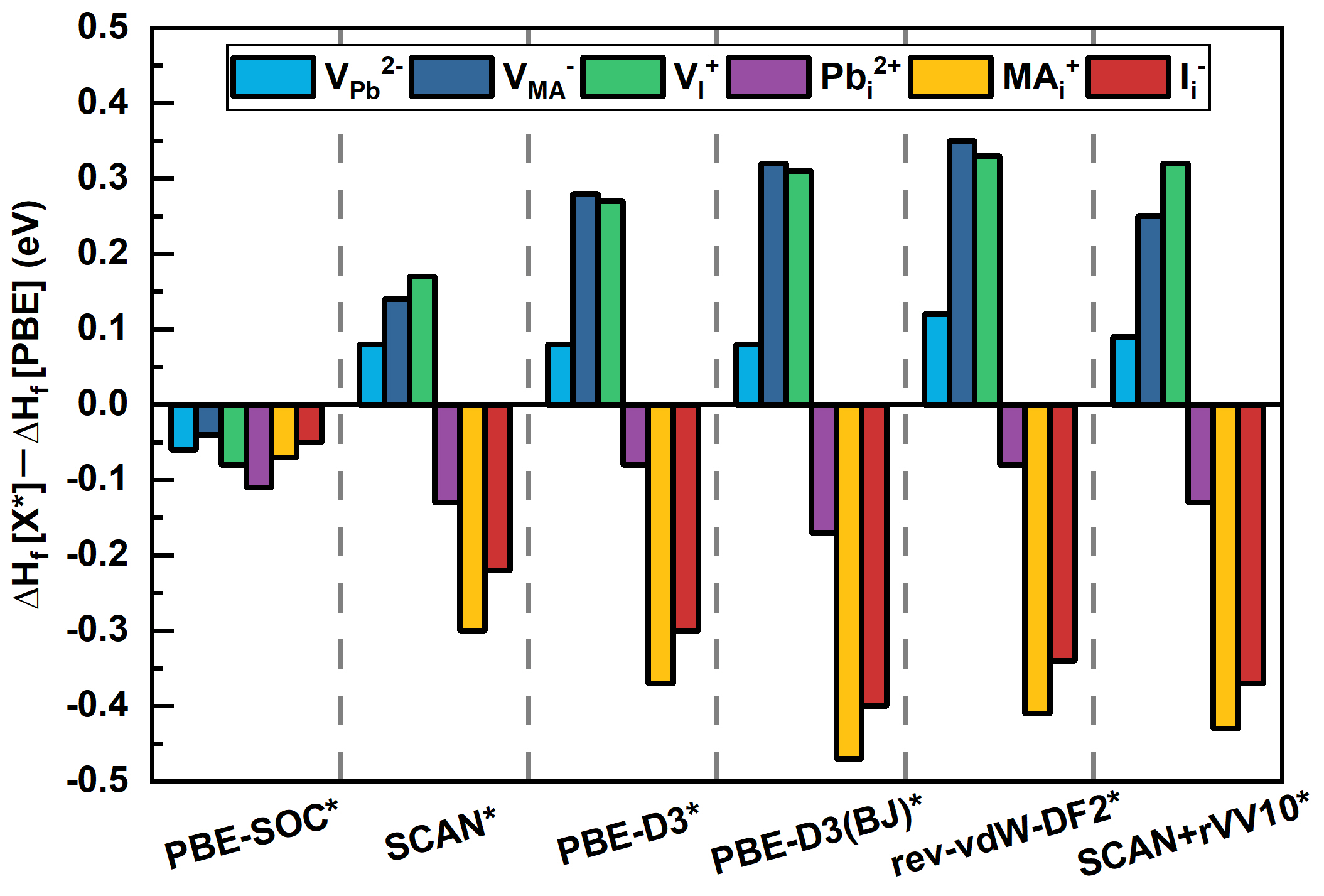
This figure demonstrates that adding SOC, while holding on to the PBE functional, leads to relatively small changes in the DFEs. SOC decreases the DFEs of all elementary vacancy and interstitial point defects by - eV. Moreover, switching to the SCAN functional, the differences between the DFEs calculated with and without SOC, are very similar to those obtained by PBE, as is illustrated by Table 1. This indicates (i) that the effect of SOC on the DFEs is small, and (ii) that it can be added as an a posteriori correction.
| Functional | ||||||
|---|---|---|---|---|---|---|
| PBE-SOC | ||||||
| SCAN-SOC |
In contrast, adding vdW corrections to PBE (PBE-D3, PBE-D3(BJ)), or using a vdW functional (rev-vdW-DF2), brings significant changes of up to eV to the DFEs, see Fig. 4. All interstitials are stabilized, whereas all vacancies are destabilized. Van der Waals interactions generally increase the bonding strength between atoms, molecules, and ions, which makes it easier to insert one of these in an existing lattice, and more difficult to extract one. Comparing the effect of adding vdW interactions on the DFEs of specific defects, one notices that the DFE changes of Pb interstitials and vacancies are only eV, whereas MA and iodine vacancies and interstitials are (de)stabilized by 0.3 to 0.4 eV.
The SCAN functional is reported to capture intermediate-range vdW-type interactions [37], which is confirmed by Fig. 4. Compared to PBE, SCAN corrects the DFEs in the same direction as adding explicit vdW terms does, i.e., it stabilizes interstitials and destabilizes vacancies, albeit quantitatively to a lesser extend. Adding on top of this explicit long-range vdW interactions, as in SCAN+rVV10, then enhances these corrections.
III.3 Structure optimizations
As a next step we consider optimization of the structure with each functional. Figure 5(a) shows the changes in the DFEs upon structure optimization, using the PBE-optimized structures as a reference. The DFEs of vacancies are only mildly affected; becomes more stable by eV, becomes less stable by eV, and is barely affected at all. In contrast, the DFEs of interstitials become significantly larger upon structure optimization by eV.
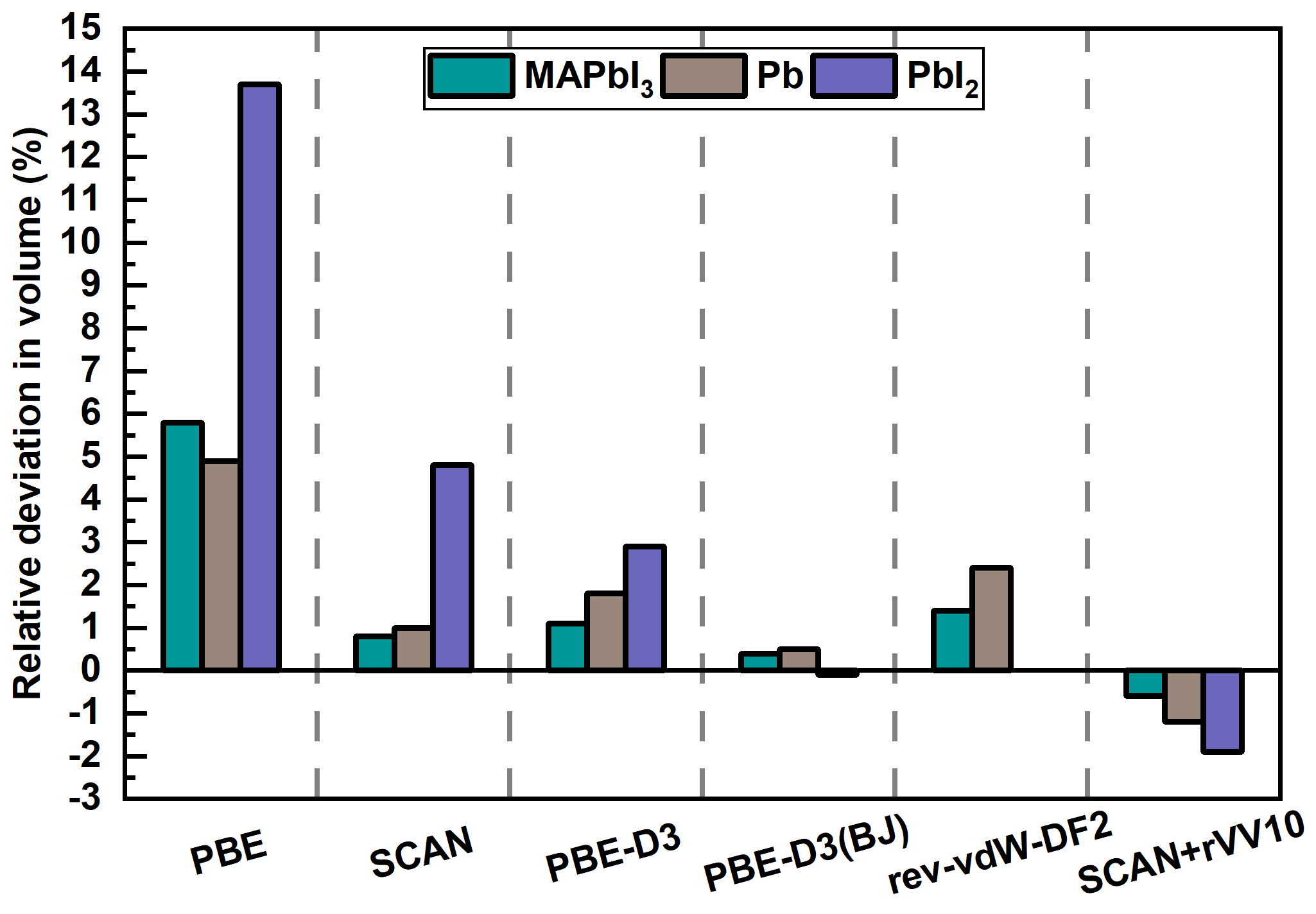
We correlate this markedly asymmetric behavior of vacancies and interstitials to differences in lattice volumes calculated with PBE, or with any of the other functionals. The deviation from the experimental value [66] of the optimized volume of MAPbI3 is shown in Fig. 6. For comparison, also shown in this figure are the corresponding deviations for PbI2 and Pb metal [67, 68]. Immediately obvious is that PBE significantly overestimates the volume of MAPbI3 by %. In this respect, the other functionals perform much better, as they give a notable improvement to volumes within 0.5-1.5% of the experimental value. It should be noticed that the differences in volume are not accompanied by large changes in the bond distance or strength of the Pb-I bonds. Instead, the volume changes are mainly incorporated by changes of I-Pb-I angles, which leads to tilting of PbI6 octahedra.
Similarly, PBE overestimates the volume of Pb metal by %, and the other functionals bring this deviation down to 0.5-2%. PbI2 is somewhat special, as it is a layered compound, which requires inclusion of vdW terms to capture the interaction between the two-dimensional PbI2 layers. Not surprisingly then, PBE overestimates the PbI2 volume by %, as it lacks these terms. Including D3 vdW terms corrects this to %, whereas the D3(BJ) vdW terms and the rev-vdW-DF2 functional reproduce the experimental value more or less exactly. The PBE error is more than halved by the SCAN functional regarding the volume of PbI2, confirming the notion that SCAN captures some of the intermediate-range vdW attraction [37]. However, capturing the longer range interactions requires adding explicit long-range vdW terms, such as rVV10. The SCAN+rVV10 functional overshoots the correction a little, and gives a volume of PbI2 that is % too small. More details about the optimized lattice parameters can be found in the Supplemental information, Tables S1 and S2.
Relating these volume changes to the DFEs, one observes that, compared to PBE, all other functionals in Fig. 6 give a markedly smaller volume for the MAPbI3 lattice. One might expect that it becomes more difficult to insert an additional cation or anion in a smaller lattice, which explains why the DFEs of interstitials increases if optimizing the lattice starting from the PBE volume. The vacancies are generally much less affected by volume changes, as they can more easily be compensated by changes in I-Pb-I angles, and tilting of octahedra.
The changes in the DFEs, calculated via self-consistent structure optimization with the different functionals, with respect to the PBE-calculated results, are shown in Fig. 5(b). They show a similar qualitative trend as the results shown in Fig. 4, which were obtained without structure optimization, i.e., vacancies are less stable and interstitials are generally more stable. However, in particular for interstitials the size of these changes is notably smaller if structure optimization is included. The change for becomes eV, whereas becomes more stable by 0.05-0.25 eV. Remarkably, the largest effect is for , which is stabilized by 0.1-0.3 eV.
In general, SCAN gives DFEs that are within 0.15 eV of PBE, although the changes for vacancies and interstitials tend to be of opposite sign. Including vdW interactions enlarges these changes up to 0.3 eV, while maintaining the same trend. This number is still notably smaller than what is obtained without structure optimization, which emphasizes the importance of performing structure optimization self-consistently if switching the functional.
III.4 Defect formation energies and concentrations
| Functional | ||||||
|---|---|---|---|---|---|---|
| Defect formation energy (eV) | ||||||
| PBE | 0.56 | 0.36 | 0.38 | 0.72 | 0.65 | 0.67 |
| PBE-SOC* | 0.52 | 0.30 | 0.31 | 0.67 | 0.55 | 0.61 |
| SCAN | 0.68 | 0.50 | 0.51 | 0.61 | 0.74 | 0.61 |
| PBE-D3 | 0.86 | 0.47 | 0.55 | 0.48 | 0.70 | 0.51 |
| PBE-D3(BJ) | 0.89 | 0.47 | 0.63 | 0.44 | 0.71 | 0.45 |
| rev-vdW-DF2 | 0.91 | 0.45 | 0.66 | 0.42 | 0.72 | 0.43 |
| SCAN+rVV10 | 0.81 | 0.50 | 0.61 | 0.47 | 0.71 | 0.48 |
| Defect concentration (cm-3) | ||||||
| PBE | 1.27 | 2.83 | 5.66 | 7.74 | 1.17 | 7.58 |
| PBE-SOC* | 7.66 | 3.93 | 7.87 | 7.67 | 6.16 | 6.58 |
| SCAN | 1.39 | 1.45 | 2.89 | 6.46 | 4.28 | 6.01 |
| PBE-D3 | 1.58 | 4.63 | 6.44 | 1.18 | 2.22 | 3.19 |
| PBE-D3(BJ) | 3.95 | 4.57 | 3.41 | 4.12 | 1.37 | 3.21 |
| rev-vdW-DF2 | 1.89 | 1.18 | 8.84 | 9.64 | 1.08 | 7.28 |
| SCAN+rVV10 | 8.68 | 1.44 | 6.10 | 1.37 | 1.59 | 1.09 |
The DFEs under intrinsic conditions and the equilibrium concentrations of the elementary point defects in MAPbI3, calculated with the different functionals including self-consistent structure optimization, are given in Fig. 7. For comparison, the DFEs calculated by different functionals based on PBE-optimized structures are shown in Figure S5. As we have argued in the previous section, in order to obtain accurate results, it is important to perform a self-consistent structure optimization for each functional.
As discussed in Sec. III.1, the PBE functional yields the lowest DFEs for the standard Schottky defects and , whereas the DFEs of the other point defects are significantly larger. In terms of equilibrium concentrations, this means that and are the dominant effects by far. Adding SOC gives little change; all DFEs are slightly reduced, increasing equilibrium concentrations by roughly an order of magnitude, but maintaining approximately the ratios between different defects. As argued in Sec. III.2, adding SOC has the same effect also for other functionals.
Using the SCAN functional, one observes that the DFEs of the Schottky defects and still are the smallest, but they are somewhat larger than those obtained with PBE, so that their equilibrium concentration is roughly two orders of magnitude smaller. In addition, the SCAN DFEs of the interstitials and , although still larger than the vacancy DFEs, have become smaller, such that their equilibrium concentrations are within a factor of fifty or so from that of the vacancies.
Adding vdW interactions (PBE-D3, PBE-D3(BJ), rev-vdW-DF2, SCAN+rVV10) enforces this trend. In fact, the DFEs of the interstitials and are now the smallest of all points defects, where only the DFE of the lead vacancy, , has a similar magnitude. This implies that and have the largest equilibrium concentrations, with the concentration being of the same order of magnitude. The equilibrium concentration of the iodine vacancy is typically two to four orders of magnitude smaller, and the concentrations of and are even smaller.
There are small differences between the results calculated with the different functionals that include vdW interactions, but the DFEs calculated with PBE-D3(BJ), rev-vdW-DF2 and SCAN+rVV10 are within eV of one another, and even PBE-D3 gives values that are quite close. The calculated densities of dominant defects fall in the range - cm-3, which is consistent with the experimentally reported range of values [5, 6, 7, 8, 9, 10].
III.5 Changing the Fermi level
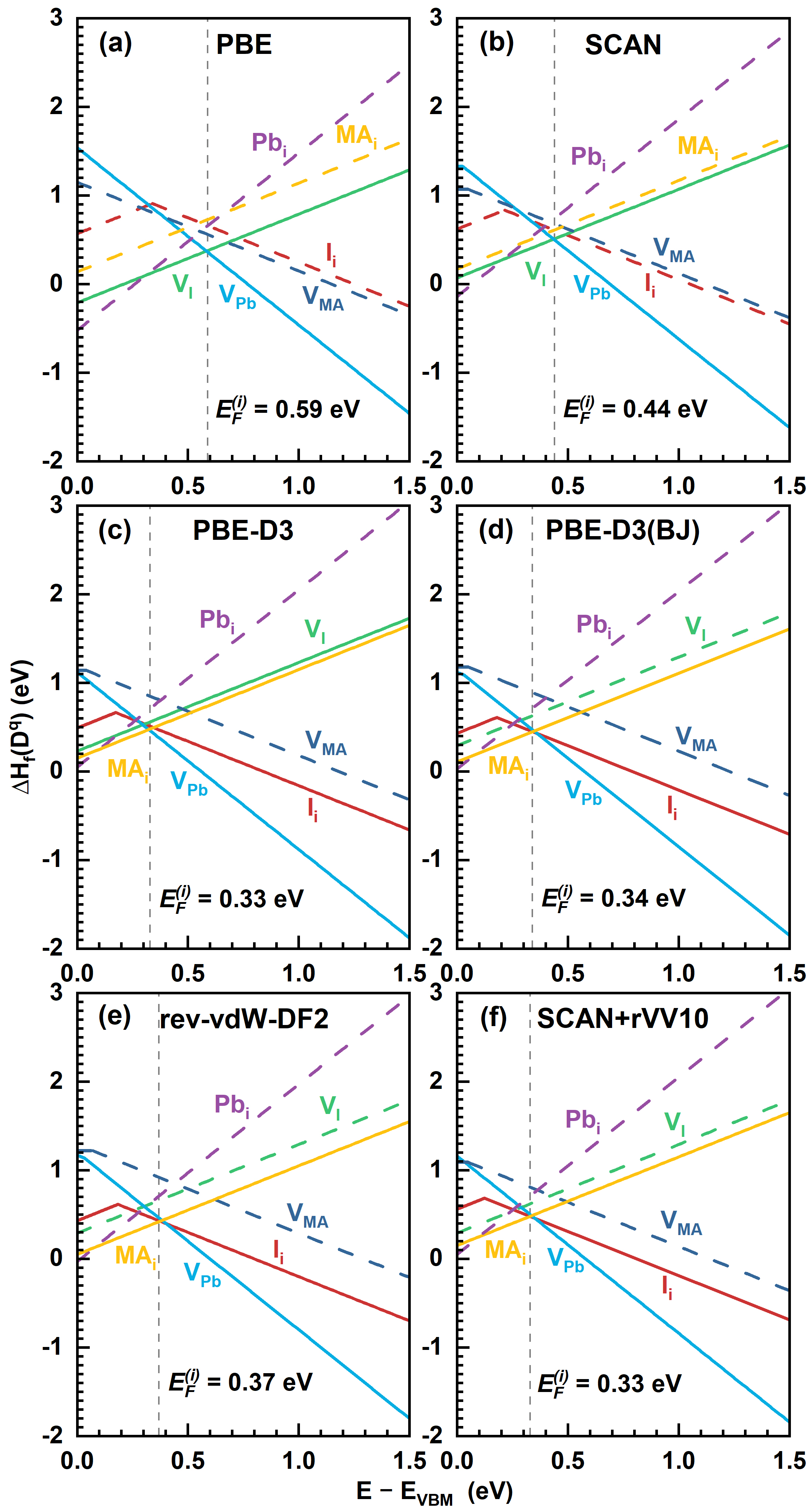
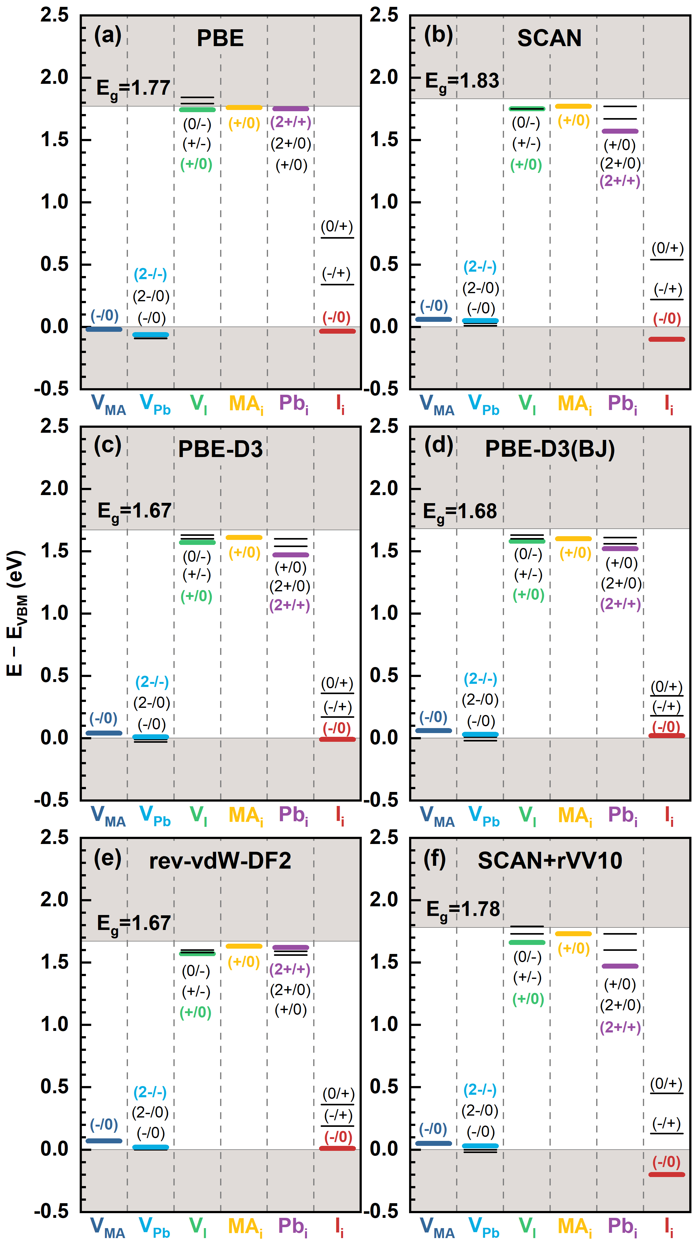
Figure 7 displays the DFEs as a function of the position of the Fermi level , calculated with full structure optimization. Results obtained with PBE-optimized structures are shown in the Supplemental Information, Figs. S5 and S6. Figure 7 demonstrates the differences between the DFEs calculated with different functionals, discussed in the previous section. In particular, at the intrinsic Fermi levels (the dashed vertical lines in Fig. 7) the interstitials and and the vacancy have the smallest DFE for the functionals that include vdW interactions, whereas without vdW interactions the vacancies and have the smaller DFE. The figure also illustrates that most defects stay in the same charge states over a large range of . Only the iodine interstitial, , shows a change from to charge at well inside the gap (varying from 0.1 eV above the VBM for SCAN+rVV10 to 0.3 eV above VBM for PBE).
Using such results, the CSTLs can be determined for all point defects for all functionals used. The results are shown in Fig. 8. One can observe that the CSTLs of most defects are close to the band edges for all functionals, implying that they are shallow traps, which is consistent with the common notion that electronically MAPbI3 is defect tolerant [11, 69, 4]. One exception is , where the CSTLs and are well inside the gap for all functionals. However, the CSTL is inactive under device operating conditions, as it requires the simultaneous capture of two charge carriers of the same type, which is highly unlikely. Meggiolaro et al. have argued that the CSTL is also inactive under these conditions, as it involves a considerable structural change accompanied by an energy barrier [51]. This remains true for all functionals tested here.
A second exception is (2+/+) CSTL of calculated with SCAN or SCAN+rVV10, at 0.26 eV and 0.31 eV below the CBM, respectively, which is somewhat too deep to be termed a shallow trap. However, the concentration of defects will be extremely small due to its large DFE.
IV Summary and conclusions
We have studied the intrinsic point defects, vacancies and interstitials, in the archetype organometal hybrid perovskite, MAPbI3, by means of DFT calculations, employing a wide range of functionals. Although such defects do not seem to hamper the electronic operation of perovskite solar cells, they are vital in understanding the instabilities and degradation mechanisms of perovskite materials. Identifying the dominant defects from DFT calculations is hampered by the fact that different functionals give different results. Using the standard PBE (GGA) functional as a starting point, we have systematically investigated the effects of adding Van der Waals (vdW) interactions, either in simple parametrized form (D3, D3(BJ)), or as non-local functional (rev-vdW-DF2, rVV10), switching to meta-GGA (SCAN), as well as including spin-orbit coupling (SOC).
Besides on the parent material MAPbI3, defect formations energies (DFEs) depend on the chemical potentials of the elements involved, and in case of charged defects, on the position of the Fermi level, which draws in inaccuracies in thermodynamic (formation enthalpies), as well as electronic properties (band positions), caused by DFT functionals. Focusing on intrinsic thermodynamic conditions, we show that the DFEs of MAPbI3 are relatively insensitive to these inaccuracies. The same will hold for other organometal hybrid perovskites.
Nevertheless, different functionals present different defects as most common. Whereas PBE predicts the standard Schottky defects, iodine and lead vacancies, and , to be dominant, including vdW interactions favors the iodine and methylammonium interstitials, and , besides lead vacancies, . In general, vdW interactions stabilize interstitials, and destabilize vacancies.
In addition, we conclude that self-consistent structural optimization is important in order to obtain accurate DFEs. We correlate this outcome to a difference in equilibrium volume found for MAPbI3 by the different functionals. PBE in particular gives a volume that is too large. If one adds vdW interactions without reoptimizing the structure and volume, one overestimates the stability of interstitials in particular.
The meta-GGA (SCAN) functional performs overall better than GGA (PBE), evidenced by the consistent improvements in lattice parameters of the relevant perovskite (MAPbI3) and precursor (PbI2). However, regarding DFEs, SCAN only captures part of the non-bonding interactions between the organic cations and the inorganic iodine and lead ions, and we suggest to include long-range vdW interactions in the form of SCAN+rVV10. Adding vdW terms to PBE, D3(BJ) in particular, or using the vdW functional rev-vdW-DF2 also gives decent DFEs. However, given the proven versatility of SCAN to accurately describe a large variety of compounds and molecules in different bonding configurations, we express a preference for the SCAN+rVV10 functional.
In contrast, the inclusion of SOC gives only relatively small and consistent corrections to the DFEs, which can be added straightforwardly as a post-correction.
Acknowledgements.
H. Xue acknowledges the funding from the China Scholarship Council (CSC). S. Tao acknowledges funding by the Computational Sciences for Energy Research (CSER) tenure track program of Shell and NWO (Project number 15CST04-2) and the NWO START-UP grant from the Netherlands.References
- Kojima et al. [2009] A. Kojima, K. Teshima, Y. Shirai, and T. Miyasaka, Journal of the American Chemical Society 131, 6050 (2009).
- National Renewable Energy Laboratory [2021] National Renewable Energy Laboratory, Best Research-Cell Efficiency Chart (2021).
- Zakutayev et al. [2014] A. Zakutayev, C. M. Caskey, A. N. Fioretti, D. S. Ginley, J. Vidal, V. Stevanovic, E. Tea, and S. Lany, The Journal of Physical Chemistry Letters 5, 1117 (2014).
- Steirer et al. [2016] K. X. Steirer, P. Schulz, G. Teeter, V. Stevanovic, M. Yang, K. Zhu, and J. J. Berry, ACS Energy Letters 1, 360 (2016).
- Adinolfi et al. [2016] V. Adinolfi, M. Yuan, R. Comin, E. S. Thibau, D. Shi, M. I. Saidaminov, P. Kanjanaboos, D. Kopilovic, S. Hoogland, Z.-H. Lu, O. M. Bakr, and E. H. Sargent, Advanced Materials 28, 3406 (2016).
- Leijtens et al. [2016] T. Leijtens, G. E. Eperon, A. J. Barker, G. Grancini, W. Zhang, J. M. Ball, A. R. S. Kandada, H. J. Snaith, and A. Petrozza, Energy Environ. Sci. 9, 3472 (2016).
- Chen et al. [2016] Y. Chen, H. T. Yi, X. Wu, R. Haroldson, Y. N. Gartstein, Y. I. Rodionov, K. S. Tikhonov, A. Zakhidov, X. Y. Zhu, and V. Podzorov, Nature Communications 7, 12253 (2016).
- de Quilettes et al. [2015] D. W. de Quilettes, S. M. Vorpahl, S. D. Stranks, H. Nagaoka, G. E. Eperon, M. E. Ziffer, H. J. Snaith, and D. S. Ginger, Science 348, 683 LP (2015).
- Blancon et al. [2016] J.-C. Blancon, W. Nie, A. J. Neukirch, G. Gupta, S. Tretiak, L. Cognet, A. D. Mohite, and J. J. Crochet, Advanced Functional Materials 26, 4283 (2016).
- Samiee et al. [2014] M. Samiee, S. Konduri, B. Ganapathy, R. Kottokkaran, H. A. Abbas, A. Kitahara, P. Joshi, L. Zhang, M. Noack, and V. Dalal, Applied Physics Letters 105, 153502 (2014).
- Yin et al. [2014] W.-J. Yin, T. Shi, and Y. Yan, Applied Physics Letters 104, 63903 (2014).
- Shi et al. [2015] T. Shi, W.-J. Yin, F. Hong, K. Zhu, and Y. Yan, Applied Physics Letters 106, 103902 (2015).
- Lindblad et al. [2014] R. Lindblad, D. Bi, B.-w. Park, J. Oscarsson, M. Gorgoi, H. Siegbahn, M. Odelius, E. M. J. Johansson, and H. Rensmo, The Journal of Physical Chemistry Letters 5, 648 (2014).
- Chen et al. [2014] Q. Chen, H. Zhou, T.-B. Song, S. Luo, Z. Hong, H.-S. Duan, L. Dou, Y. Liu, and Y. Yang, Nano Letters 14, 4158 (2014).
- Sadoughi et al. [2015] G. Sadoughi, D. E. Starr, E. Handick, S. D. Stranks, M. Gorgoi, R. G. Wilks, M. Bär, and H. J. Snaith, ACS Applied Materials & Interfaces 7, 13440 (2015).
- Wang et al. [2017] S. Wang, Y. Jiang, E. J. Juarez-Perez, L. K. Ono, and Y. Qi, Nature Energy 2, 16195 (2017).
- Jiang et al. [2018] J. Jiang, C. K. Onwudinanti, R. A. Hatton, P. A. Bobbert, and S. Tao, The Journal of Physical Chemistry C 122, 17660 (2018).
- Fang et al. [2018] H.-H. Fang, J. Yang, S. Tao, S. Adjokatse, M. E. Kamminga, J. Ye, G. R. Blake, J. Even, and M. A. Loi, Advanced Functional Materials 28, 1800305 (2018).
- Motti et al. [2019] S. G. Motti, D. Meggiolaro, A. J. Barker, E. Mosconi, C. A. R. Perini, J. M. Ball, M. Gandini, M. Kim, F. De Angelis, and A. Petrozza, Nature Photonics 13, 532 (2019).
- Li et al. [2019] N. Li, S. Tao, Y. Chen, X. Niu, C. K. Onwudinanti, C. Hu, Z. Qiu, Z. Xu, G. Zheng, L. Wang, Y. Zhang, L. Li, H. Liu, Y. Lun, J. Hong, X. Wang, Y. Liu, H. Xie, Y. Gao, Y. Bai, S. Yang, G. Brocks, Q. Chen, and H. Zhou, Nature Energy 4, 408 (2019).
- Li et al. [2020] N. Li, Y. Luo, Z. Chen, X. Niu, X. Zhang, J. Lu, R. Kumar, J. Jiang, H. Liu, X. Guo, B. Lai, G. Brocks, Q. Chen, S. Tao, D. P. Fenning, and H. Zhou, Joule 4, 1743 (2020).
- Chen et al. [2019] B. Chen, P. N. Rudd, S. Yang, Y. Yuan, and J. Huang, Chemical Society Reviews 48, 3842 (2019).
- Son et al. [2016] D.-Y. Son, J.-W. Lee, Y. J. Choi, I.-H. Jang, S. Lee, P. J. Yoo, H. Shin, N. Ahn, M. Choi, D. Kim, and N.-G. Park, Nature Energy 1, 16081 (2016).
- Bi et al. [2016] D. Bi, W. Tress, M. I. Dar, P. Gao, J. Luo, C. Renevier, K. Schenk, A. Abate, F. Giordano, J.-P. Correa Baena, J.-D. Decoppet, S. M. Zakeeruddin, M. K. Nazeeruddin, M. Grätzel, and A. Hagfeldt, Science Advances 2, e1501170 (2016).
- Bi et al. [2014] C. Bi, Y. Shao, Y. Yuan, Z. Xiao, C. Wang, Y. Gao, and J. Huang, J. Mater. Chem. A 2, 18508 (2014).
- Dualeh et al. [2014] A. Dualeh, N. Tétreault, T. Moehl, P. Gao, M. K. Nazeeruddin, and M. Grätzel, Advanced Functional Materials 24, 3250 (2014).
- de Walle and Neugebauer [2004] C. G. V. de Walle and J. Neugebauer, Journal of Applied Physics 95, 3851 (2004).
- Freysoldt et al. [2014] C. Freysoldt, B. Grabowski, T. Hickel, J. Neugebauer, G. Kresse, A. Janotti, and C. G. Van de Walle, Reviews of Modern Physics 86, 253 (2014).
- Perdew et al. [1996] J. P. Perdew, K. Burke, and M. Ernzerhof, Phys. Rev. Lett. 77, 3865 (1996).
- Tran et al. [2016] F. Tran, J. Stelzl, and P. Blaha, The Journal of Chemical Physics 144, 204120 (2016).
- Zhang et al. [2018a] Y. Zhang, D. A. Kitchaev, J. Yang, T. Chen, S. T. Dacek, R. A. Sarmiento-Pérez, M. A. L. Marques, H. Peng, G. Ceder, J. P. Perdew, and J. Sun, npj Computational Materials 4, 9 (2018a).
- Zhang et al. [2018b] G.-X. Zhang, A. M. Reilly, A. Tkatchenko, and M. Scheffler, New Journal of Physics 20, 063020 (2018b).
- Stroppa and Kresse [2008] A. Stroppa and G. Kresse, New Journal of Physics 10, 063020 (2008).
- Stevanović et al. [2012] V. Stevanović, S. Lany, X. Zhang, and A. Zunger, Physical Review B 85, 115104 (2012).
- Peng et al. [2013] H. Peng, D. O. Scanlon, V. Stevanovic, J. Vidal, G. W. Watson, and S. Lany, Physical Review B 88, 115201 (2013).
- Sun et al. [2015] J. Sun, A. Ruzsinszky, and J. Perdew, Physical Review Letters 115, 36402 (2015).
- Sun et al. [2016] J. Sun, R. C. Remsing, Y. Zhang, Z. Sun, A. Ruzsinszky, H. Peng, Z. Yang, A. Paul, U. Waghmare, X. Wu, M. L. Klein, and J. P. Perdew, Nature Chemistry 8, 831 (2016).
- Yang et al. [2019] J. H. Yang, D. A. Kitchaev, and G. Ceder, Physical Review B 100, 035132 (2019).
- Grimme et al. [2010] S. Grimme, J. Antony, S. Ehrlich, and H. Krieg, Journal of Chemical Physics 132, 10.1063/1.3382344 (2010).
- Grimme et al. [2011] S. Grimme, S. Ehrlich, and L. Goerigk, Journal of Computational Chemistry 32, 1456 (2011).
- Hamada [2014] I. Hamada, Phys. Rev. B 89, 121103 (2014).
- Klimeš et al. [2011] J. c. v. Klimeš, D. R. Bowler, and A. Michaelides, Phys. Rev. B 83, 195131 (2011).
- Dion et al. [2004] M. Dion, H. Rydberg, E. Schröder, D. C. Langreth, and B. I. Lundqvist, Phys. Rev. Lett. 92, 246401 (2004).
- Román-Pérez and Soler [2009] G. Román-Pérez and J. M. Soler, Phys. Rev. Lett. 103, 096102 (2009).
- Tran et al. [2019] F. Tran, L. Kalantari, B. Traoré, X. Rocquefelte, and P. Blaha, Physical Review Materials 3, 63602 (2019).
- Meggiolaro and De Angelis [2018] D. Meggiolaro and F. De Angelis, ACS Energy Letters 3, 2206 (2018).
- Agiorgousis et al. [2014] M. L. Agiorgousis, Y.-Y. Sun, H. Zeng, and S. Zhang, Journal of the American Chemical Society 136, 14570 (2014).
- Buin et al. [2014] A. Buin, P. Pietsch, J. Xu, O. Voznyy, A. H. Ip, R. Comin, and E. H. Sargent, Nano Letters 14, 6281 (2014).
- Buin et al. [2015] A. Buin, R. Comin, J. Xu, A. H. Ip, and E. H. Sargent, Chemistry of Materials 27, 4405 (2015).
- Ming et al. [2016] W. Ming, S. Chen, and M.-H. Du, Journal of Materials Chemistry A 4, 16975 (2016).
- Meggiolaro et al. [2018a] D. Meggiolaro, S. G. Motti, E. Mosconi, A. J. Barker, J. Ball, C. Andrea Riccardo Perini, F. Deschler, A. Petrozza, and F. De Angelis, Energy & Environmental Science 11, 702 (2018a).
- Meggiolaro et al. [2018b] D. Meggiolaro, E. Mosconi, and F. De Angelis, ACS Energy Letters 3, 447 (2018b).
- Pols et al. [2021] M. Pols, J. M. Vicent-Luna, I. Filot, A. C. T. van Duin, and S. Tao, The Journal of Physical Chemistry Letters 12, 5519 (2021).
- Bokdam et al. [2017] M. Bokdam, J. Lahnsteiner, B. Ramberger, T. Schäfer, and G. Kresse, Physical Review Letters 119, 145501 (2017).
- Lahnsteiner et al. [2018] J. Lahnsteiner, G. Kresse, J. Heinen, and M. Bokdam, Physical Review Materials 2, 073604 (2018).
- Sabatini et al. [2013] R. Sabatini, T. Gorni, and S. de Gironcoli, Physical Review B 87, 041108 (2013).
- Peng et al. [2016] H. Peng, Z.-H. Yang, J. P. Perdew, and J. Sun, Physical Review X 6, 41005 (2016).
- Even et al. [2013] J. Even, L. Pedesseau, J.-M. Jancu, and C. Katan, The Journal of Physical Chemistry Letters 4, 2999 (2013).
- Kresse and Hafner [1993] G. Kresse and J. Hafner, Physical Review B 47, 558 (1993).
- Kresse and Furthmüller [1996a] G. Kresse and J. Furthmüller, Physical Review B 54, 11169 (1996a).
- Kresse and Furthmüller [1996b] G. Kresse and J. Furthmüller, Computational Materials Science 6, 15 (1996b).
- Yang et al. [2015] J.-H. Yang, W.-J. Yin, J.-S. Park, and S.-H. Wei, Scientific Reports 5, 16977 (2015).
- Tress [2017] W. Tress, Advanced Energy Materials 7, 1602358 (2017).
- Park et al. [2018] J. S. Park, S. Kim, Z. Xie, and A. Walsh, Nature Reviews Materials 3, 194 (2018).
- Du [2015] M.-H. Du, The Journal of Physical Chemistry Letters 6, 1461 (2015).
- Stoumpos et al. [2013] C. C. Stoumpos, C. D. Malliakas, and M. G. Kanatzidis, Inorganic Chemistry 52, 9019 (2013).
- Vishan and Narlikar [1976] V. Vishan and A. Narlikar, Materials Research Bulletin 11, 1257 (1976).
- Flahaut et al. [2006] E. Flahaut, J. Sloan, S. Friedrichs, A. I. Kirkland, K. S. Coleman, V. C. Williams, N. Hanson, J. L. Hutchison, and M. L. H. Green, Chemistry of Materials 18, 2059 (2006).
- Walsh et al. [2015] A. Walsh, D. O. Scanlon, S. Chen, X. G. Gong, and S.-H. Wei, Angewandte Chemie International Edition 54, 1791 (2015).