Calibration of the scintillation of cerium-doped yttrium aluminum garnet crystals irradiated by monoenergetic 4 MeV energy electrons
Abstract
This paper presents the results of measurements of fluorescing cerium-doped yttrium aluminum garnet crystals after being irradiated by an accelerated electron beam with energy of around 4 MeV. The measurements were performed using the PHIL linear accelerator at LAL (France). We observe linear dependence of the crystal emission to the electron beam charge and the isotropy of the photon emission. We provide the calibration coefficients of the photon emission depending on the charge of the accelerated electron beam for two crystals originating from two different manufacturers.
1 Introduction
Cerium-doped yttrium aluminum garnet (YAG:Ce) is a scintillation material produced in a form of single-crystal of composition Y3Al5O12. It emits yellow light with maximum emission at 550 nm wavelength when subjected to ionising radiation (UV, x-rays, charged particles). Fluorescence decay time is composed of a fast decay time of 70 ns and a slower decay time of the order of s [1, 2]. YAG:Ce scintillators are used in a wide range of applications, including cathode tubes, PET scanners, high-energy gamma radiation and charged particle detectors, and high-resolution imaging screens for gamma, x-rays, beta radiation and ultraviolet radiation [3, 4, 5].
For laser-plasma interaction experiments, such as those widely performed at petawatt-class laser facilities [6], YAG:Ce scintillators can be used as end detectors in magnetic spectrometers of ionizing radiation. With the democratisation of high repetition rate Petawatt-class laser facilities (state-of-art lasers, such as Apollon [7], Vega [8] and ELI-NP [9] are capable of delivering optical pulses to a target chamber with one shot per minute repetition rate), fast reusable detectors are needed to optimize the efficiency of particle and radiation detection.
Currently single-use detectors (such as Image Plate[10, 11] and CR-39[12]) are used in laser-plasma interaction experiments. They are not compatible with high repetition rate as they need to be replaced after each shot. A good candidate for particles detection produced during such interactions is the YAG:Ce scintillating material as its fluorescence decay time is shorter than 1 s (90 ns). Another of its advantage is the minimum out gazing of the crystal compared to Lanex screen[14, 13] allowing their use in extremely high vacuum. Moreover its fluorescence emission is in the visible spectrum (maximal at 550 nm [1, 2]) which is suitable for regular CCD or CMOS devices coupled with an imaging system.
In this paper we present the results of YAG:Ce scintillators calibration performed at the linear accelerator of electrons (LAL, Orsay) [15, 16, 17]. The aim here is to calculate the photon emission response from the bulk of YAG:Ce crystal exposed to an electron beam. Two individual crystals from two different manufacturers (see Table 1) were irradiated by a collimated mono-energetic electron beam having variable energy from 3.5 MeV to 4.2 MeV and charge from 2 pC to 20 pC. The emission level was registered by BASLER CMOS cameras placed at three different angles relative to the direction of the electron beam.
2 Experimental setup description
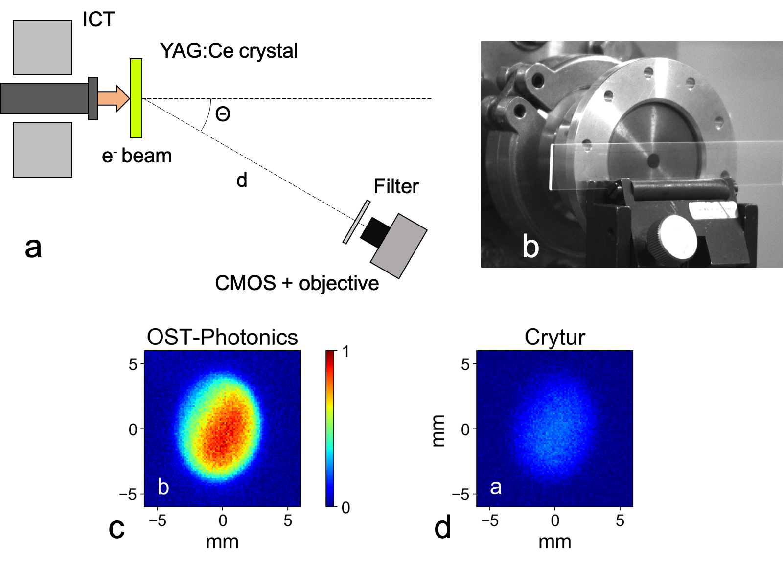
The linear electron accelerator PHIL at LAL (Laboratoire de l’accélérateur linéaire, Orsay, France), used for the calibration, provides a collimated monoenergetic beam of accelerated electrons with 1 ps duration, charge up to 20 pC, energies from 3.45 MeV to 4.2 MeV and 5 mm diameter at the output. The setup of the experiment is shown in the Figure 1. The electron beam impacted the YAG:Ce crystal sample, which was placed on the axis of its path. Two YAG:Ce crystals from two different manufacturers (see Table 1) were calibrated.
| Manufacturer | Doping fraction | Thickness | Measured light yield | |
|---|---|---|---|---|
| Crystal 1 | OST-Photonics | 2 % | 0.5 mm | 4800 photons/MeV |
| Crystal 2 | Crytur | 1 % | 1 mm | 500 photons/MeV |

The light emitted from the bulk of the crystal was registered by the 8-bit Basler ACE CMOS matrix (model acA1300-30gm) equipped with an objective lens at three angles from the electron axis and and a distance of approximately 1 m from the crystal, corresponding to a collection solid angle of 25 sr). We used a range of camera gains from minimum to maximum and two exposure times: 10 ms and 100 ms. Neutral density filters (from Thorlabs) and a narrow-band filter (central wavelength at 550 nm and 100 nm bandwidth from Edmund Optics) were used to optimize the imaging system. Examples of images obtained with this set-up are shown in Figure 1 (c, d).
The charge of the electron beam was measured by means of an Integrating Current Transformer (ICT) placed at the end of the accelerator line before the output beam collimator and the output titanium window, and by a Faraday Cup (FC) at the place of crystal mounting position (in air, after the output titanium window). The exact charge of the electron beam, impacting the YAG:Ce crystal was retrieved based on ICT measurements, with the electron transmission of the collimator and the titanium window taken into an account.
3 Results of YAG:Ce crystals calibration
During the propagation of electrons inside the bulk of the YAG:Ce crystal, electrons will make collisions with atoms, losing energy. This energy will be stored in energy levels of Ce3+. The excitation of the energy levels of the Ce will release photons in solid angle by spontaneous emissions with two characteristics decay time 70 ns and s [1, 2]. The relation between the number of emitted photons and the incident electron charge is the crystal response to the electrons (also called light yield , with being the normalized emission spectrum of the emitted photon that could be find in [2, 4], being the scintillation photon wavelength, and being the integrated light yield). It can be written as:
| (3.1) |
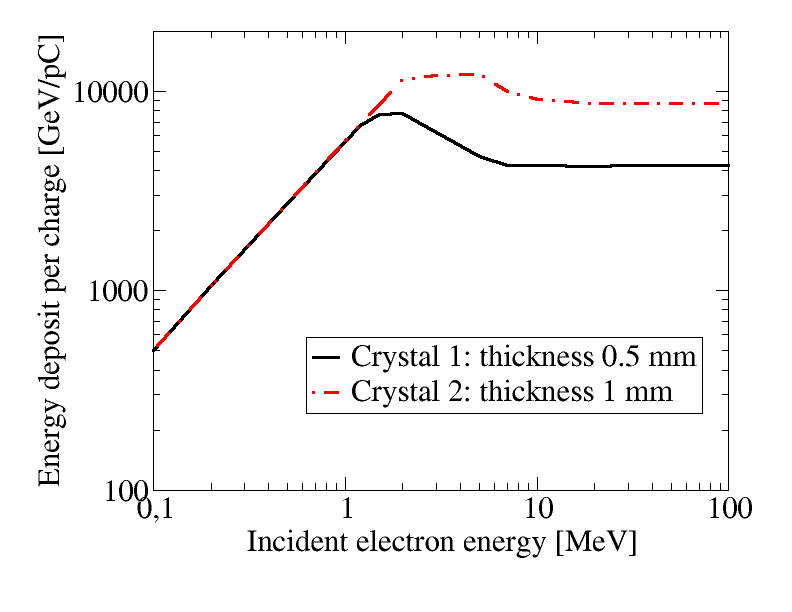
where is the total number of photons emitted by the crystal, is the deposited energy of the electron beam per pC, and is the charge of the electron beam in pC. depends on the incident electron energy and can be calculated using the GEANT4 toolkit [18, 19, 20] for different crystal compositions and thicknesses (see Figure 2).

The charge of the electron beam was obtained using the calibrated ICT measurement. The total number of photons emitted by the crystal was retrieved from the integrated crystal fluorescent image (Figure 1 (c, d)) using the equation 3.2 with an assumption of isotropic photon emission:
| (3.2) |
where corresponds to the signal from the crystal image without electron beam interacting with it, is the collection solid angle of the imaging system, is the transmission of filters in front of the camera, and correspond to the detector parameters, which in our case is the quantum efficiency of the Basler CMOS chip multiplied by the camera Gain () [21].
| (3.3) |
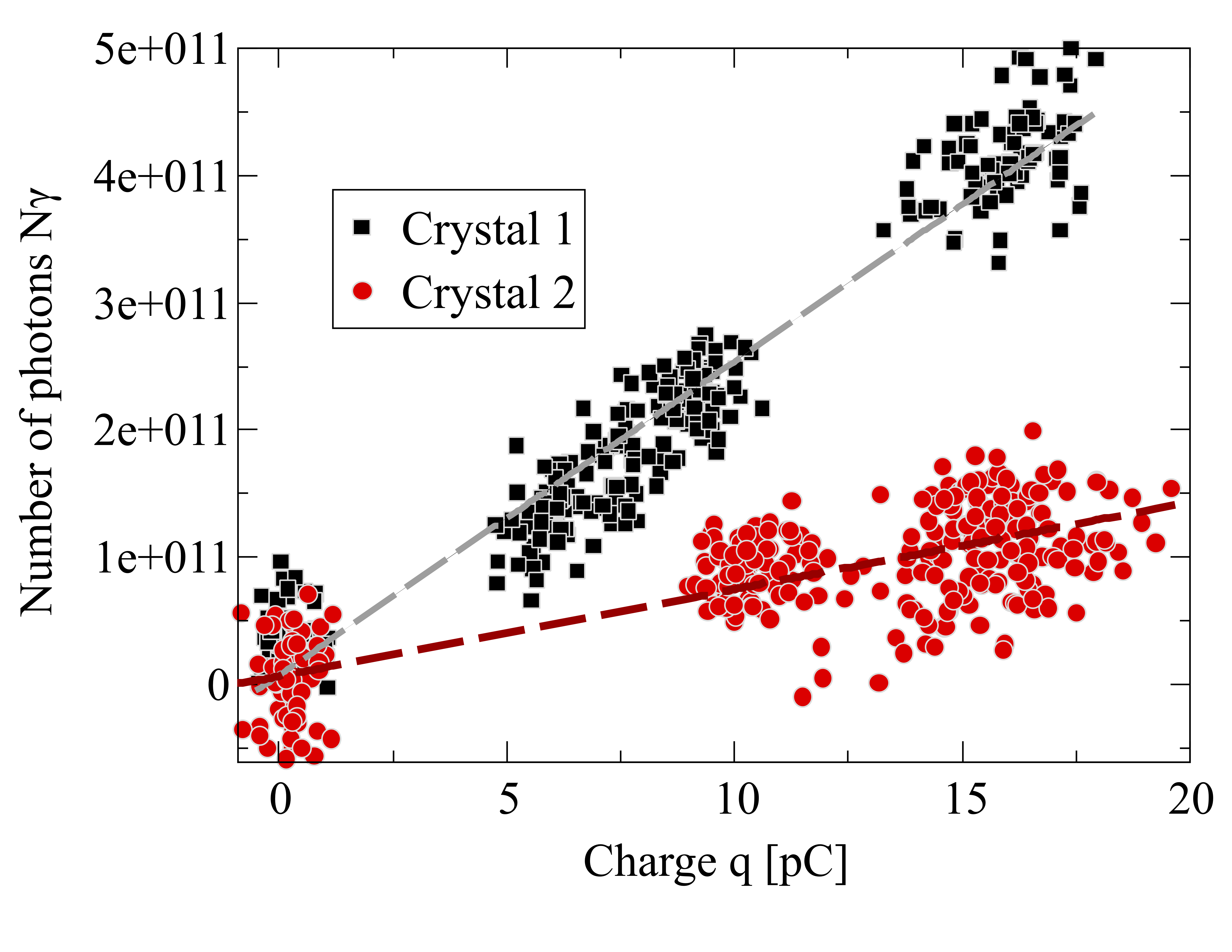
On Figure 3 we plotted the number of photons emitted by the crystal as a function of the electron beam charge for the two different crystals. It is clearly seen from the figure that the factor remains constant in the range from 1 pC to 20 pC and equals to photons/pC for the crystal 1 and photons/pC for the crystal 2. Using Figure 2 we obtained the light yield for the two crystals (see Table 1 "light yield " column).

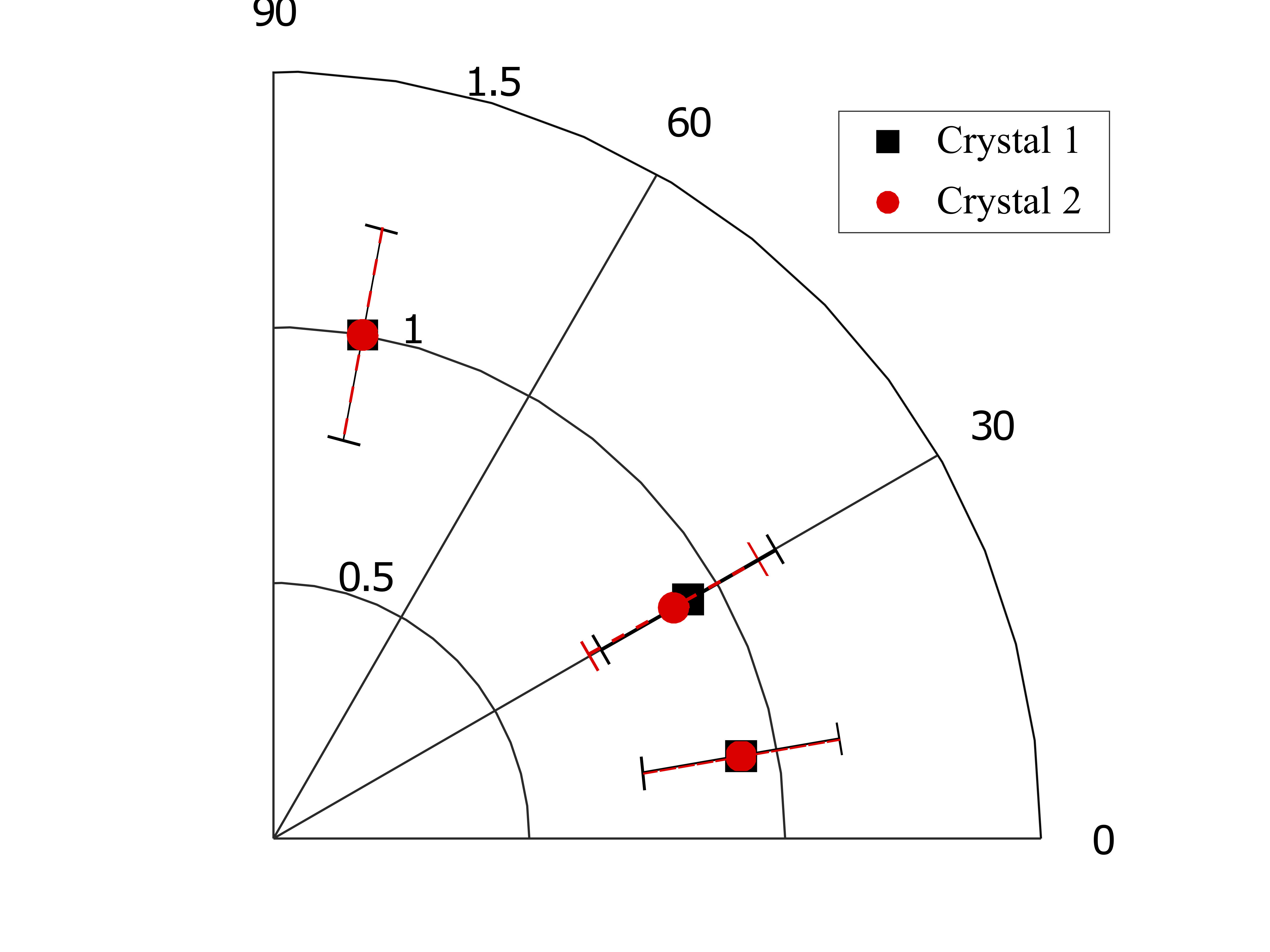
As can be seen from Figure 4, the signal level registered by the detector is independent of the angle (see Figure 1), that is in consistency with the assumption of isotropic photon emission from the crystal, used in Equation 3.3.

The measurements of the signal level with 10 times increased exposure time (100 ms) of the Basler camera did not affect the values of and factors, only increasing the grey level of the background signal (in consistency with a fluorescence decay time shorter than the acquisition time). We also changed the electron beam energy from 3.5 to 4.2 MeV. The results show similar trend and values. Those measurements were also performed for another Crytur’s YAG:Ce crystal, showing same trend and values of its response to electrons.
4 Summary
We performed the calibration of two similar YAG:Ce crystals from two different manufacturers. We observe that the response to electron is linear, that is ideal for high repetition rate electron or positron detection. In the studied range of electron charge, we did not observe saturation of the light emitted by the crystal. Our main concern is the difference of light yield from these two crystals. The difference between these two factors is close to a factor of 10. This difference cannot be directly related to the doping fraction of cesium inside of the crystal as it only a factor of 2 (see Table 1). As these crystals are from two different manufacturers, we can think of different growth processes. This highlights the necessity of performing light yield calibration for each crystal manufacturer as the response of them can be very different.
Acknowledgments
This work was supported by funding from the European Research Council (ERC) under the European Unions Horizon 2020 research and innovation program (Grant Agreement No.787539) and by funding from the Russian Science Foundation (RSF) in the frame of project No.20-62-46050.
References
- [1] G. Blasse and A. Bril, A new phosphor for flying-spot cathode-ray tubes for color television: yellow-emitting , Applied Physics Letters, 11 (1967) 53.
- [2] E. Mihóková et al., Luminescence and scintillation properties of YAG:Ce single crystal and optical ceramics, Journal of Luminescence, 126 (2007) 1.
- [3] M. van Tol and J. van Esdonk, A high luminance high-resolution cathode-ray tube for special purposes, IEEE Transactions on Electron Devices, 30 (1983) 193-197.
- [4] M. Mashlan et al., YAG:Ce and YAP:Ce – Suitable Fast Detectors for Transmission Mössbauer Spectroscopy, Hyperfine Interactions, 139 (2002) 673–678.
- [5] M. Nikl Scintillation detectors for x-rays, Measurement Science and Technology, 17 (2006) R37.
- [6] C. Danson et al., Petawatt and exawatt class lasers worldwide, High Power Laser Science and Engineering, 7 (2019) E54.
- [7] D. Papadopoulos et al., First commissioning results of the Apollon laser on the 1 PW beam line, Conference on Lasers and Electro-Optics OSA Technical Digest (2019) STu3E.4.
- [8] C. Mendez et al., VEGA laser facility beamlines management for pump-probe experiments, Proceedings of SPIE 11207, Fourth International Conference on Applications of Optics and Photonics, (2019) 112071Z.
- [9] F. Lureau et al., High-energy hybrid femtosecond laser system demonstrating 2 10 PW capability, High Power Laser Science and Engineering, 8 (2020) e43.
- [10] G. Boutoux et al., Validation of modelled imaging plates sensitivity to 1-100 keV x-rays and spatial resolution characterisation for diagnostics for the "PETawatt Aquitaine Laser"., Review of Scientific Instruments 87 043108 (2016).
- [11] J. Strehlow et al., The response function of Fujifilm BAS-TR imaging plates to laser-accelerated titanium ions, Review of Scientific Instruments 90, 083302 (2019).
- [12] T. W. Jeong et al., CR-39 track detector for multi-MeV ion spectroscopy, Scientific Reports 7, 2152 (2017).
- [13] N. Rabhi et al., Calibration of imaging plates to electrons between 40 and 180 MeV,Review of Scientific Instruments 87, 053306 (2016).
- [14] A. Buck et al., Absolute charge calibration of scintillating screens for relativistic electron detection, Review of Scientific Instruments 81, 033301 (2010).
- [15] R. Roux et al., PHIL: a Test Beam line at LAL, Proceedings of European Particle Accelerator Conference (EPAC-08), (2008) 2698-2700
- [16] J. Brossard et al., PHIL accelerator at LAL – diagnostics status, Proceedings of Beam Instrumentation Workshop (BIW-10), (2010) 446-448
- [17] J. Brossard et al., Low Energy Beam Measurements Using PHIL Accelerator at LAL, Comparison with PARMELA Simulations, 2011 Particle Accelerator Conference (PAC-11), (2011) 1885-1887
- [18] S. Agostinelli et al., Geant4—a simulation toolkit, Nuclear Instruments and Methods in Physics Research Section A: Accelerators, Spectrometers, Detectors and Associated Equipment, 506 (2003) 250-303.
- [19] J. Allison et al., Geant4 developments and applications, IEEE Transactions on Nuclear Science, 53 (2006) 270-278.
- [20] J. Allison et al., Recent developments in Geant4, Nuclear Instruments and Methods in Physics Research Section A: Accelerators, Spectrometers, Detectors and Associated Equipment, 835 (2016) 186-225.
- [21] Basler AG, Basler acA1300-30gm, camera Specification measurement protocol using the EMVA Standard 1288.