Normal Metal-Superconductor Near-Field Thermal Diodes and Transistors
Abstract
In recent years there has been a number of proposals of thermal devices operating in the near-field regime that make use of phase-transition materials. Here, we present a theoretical study of near-field thermal diodes and transistors that combine superconducting materials with normal (non-superconducting) metals. To be precise, we show that a system formed by two parallel plates made of Nb and Au can exhibit unprecedented rectification ratios very close to unity at temperatures around Nb superconducting critical temperature and for a wide range of gap size values within the near-field regime. Moreover, we also show that a superconducting Nb layer placed between Au plates can operate as a near-field thermal transistor where the amplification factor can be greatly tuned by varying different parameters such as the temperature and thickness of the Nb layer or the distance between the Nb layer and the Au plates. Overall, our work shows the potential of the use of superconductors for the realization of near-field thermal devices.
I Introduction
When two objects at different temperatures are separated by a distance smaller than the thermal wavelength given by Wien’s displacement law (10 m at room temperature), they can exchange thermal radiation via evanescent waves (or photon tunneling). Such a contribution to the near-field radiative heat transfer (NFRHT) can dominate the heat exchange for small gaps and lead to overcome the blackbody limit set by Stefan-Boltzmann’s law for the radiative heat transfer between two bodies Song2015a ; Cuevas2018 ; Biehs2020 . This NFRHT enhancement was first predicted by Polder and van Hove in the early 1970’s Polder1971 making use of the so-called theory of fluctuational electrodynamics Rytov1953 ; Rytov1989 . In recent years this idea has been thoroughly tested and confirmed in a great variety of systems and using different types of materials Kittel2005 ; Narayanaswamy2008 ; Hu2008 ; Rousseau2009 ; Shen2009 ; Shen2012 ; Ottens2011 ; Kralik2012 ; Zwol2012a ; Zwol2012b ; Guha2012 ; Worbes2013 ; Shi2013 ; St-Gelais2014 ; Song2015b ; Kim2015 ; Lim2015 ; St-Gelais2016 ; Song2016 ; Bernardi2016 ; Cui2017 ; Kloppstech2017 ; Ghashami2018 ; Fiorino2018 ; DeSutter2019 .
It is safe to say that at this stage the basic physical mechanisms underlying NFRHT are relatively well-understood. For this reason, efforts in the thermal radiation community are now shifting towards the proposal and realization of novel functional devices based on NFRHT. In this regard, a natural research line that is being pursued is the investigation of the near-field thermal analogues of the key building blocks of today’s microelectronics: diodes, transistors, switches, memory elements, etc. Thus far, the diode or rectifier has been the most widely studied thermal device. There have been a lot theoretical proposals to achieve thermal rectification that make use of systems with dissimilar materials that, in turn, exhibit optical properties that depend on temperature. The proposed material combinations include SiC structures Otey2010 , doped Si films Basu2011 , dielectric coating Iizuka2012 , and Si and a different material Wang2013 , just to mention a few. However, the most promising proposals for near-field thermal diodes are based on the use of phase-transition materials Ben-Abdallah2013 ; Yang2013 ; Huang2013 ; Nefzaoui2014 ; Yang2015 ; Ghanekar2016 ; Zheng2017 . An ideal example is that of vanadium dioxide (VO2), which undergoes a phase transition from insulator below 340 K to a metal above that temperature. This phase transition is accompanied by a drastic change in the infrared optical properties, which has a strong impact in the corresponding radiative heat transfer in systems featuring this material as the temperature is varied across the transition temperature Zwol2011a ; Zwol2011b ; Ito2017 . In fact, several experiments have already demonstrated rectification between VO2 and SiO2 in the far-field regime Zwol2012a ; Ito2017 ; Ito2014 . More importantly for our work, the first observation of thermal rectification in the near-field regime has been recently reported between a Si microdevice and a macroscopic VO2 film Fiorino2018b . In that work, a clear rectifying behavior that increased at nanoscale separations was observed with a maximum rectification ratio exceeding 50% at 140 nm gaps and a temperature difference of 70 K. This high rectification ratio was attributed to the broadband enhancement of heat transfer between metallic VO2 and doped Si surfaces, as compared to the narrower-band exchange that occurs when VO2 is in its insulating state. From the theoretical point of view, it has been shown that the rectification ratio can be boosted by nanostructuring VO2 films to form, e.g., one-dimensional gratings Ghanekar2016 ; Ghanekar2018 and the highest reported values for the rectification ratio in the near-field reach about 94% Ghanekar2016 .
In 2014, Ben-Abdallah and Biehs extended the idea of thermal diodes based on a phase-transition material to propose the realization of a near-field thermal transistor Ben-Abdallah2014 . Their proposed transistor featured a three-body system (two diodes in series) in which a layer of a metal-to-insulator transition material (the gate) is placed at subwavelength distances from two thermal reservoirs (the source and the drain). In this device, the temperatures of the reservoirs are kept fixed, while the temperature of the gate is modulated around its steady-state temperature. Making use of an extension of the theory of fluctuational electrodynamics to deal with extended many-body systems Messina2012 , Ben-Abdallah and Biehs showed that by changing the gate temperature around its critical value, the heat flux exchanged between the hot body (source) and the cold body (drain) can be reversibly switched, amplified, and modulated by a tiny action on the gate. Let us also say that these ideas have been extended to propose other key elements such as a thermal memory Kubytskyi2014 , and it has also been shown that thermal logic gates can be realized exploiting the near-field radiative interaction in -body systems with phase-transition materials Ben-Abdallah2016 . These proposals are nicely reviewed in Refs. Ben-Abdallah2017 ; Biehs2020 .
Since phase-transition materials are ideally suited for near-field thermal management devices, it is natural to think of superconductors. Although superconductors require to work at low temperatures, their use has the advantage that since the thermal wavelength is inversely proportional to temperature, the near-field regime extends to gaps beyond the millimeter scale for temperatures around 1 K. Thus, it is easy to reach gaps or separations for which the radiative heat transfer is enhanced beyond the blackbody limit. When a normal metal undergoes a superconducting phase transition (we focus here on conventional low-temperature superconductors), its optical properties change drastically in the microwave range due to the appearance of a gap in its density of states (of the order of 1 meV depending on the superconductor). This gap reduces the emissivity of the metal and in the superconducting state, one expects a substantial reduction of the NFRHT when a second material is brought in close proximity. This naive idea has been experimentally confirmed in recent years with measurements of the NFRHT between parallel plates made of superconductors like Nb and NbN Kralik2017 ; Musilova2019 . In particular, it has been reported that there is a contrast in the NFRHT between the normal and the superconducting state of a factor 5 in the case of Nb Kralik2017 and 8 in the case of NbN plates Musilova2019 . Inspired by these experiments, Ordoñez-Miranda et al. Ordonez2017 proposed the use of a low-temperature superconductor to realize a near-field thermal diode. In their proposal, the thermal reservoirs were made of Nb and SiO2 and the device operated at temperatures around the superconducting critical temperature of Nb (9 K). In particular, they found that at temperatures 1 and 8.7 K for the two thermal reservoirs, the rectification factor reached a maximum of 71% for gaps of the order of 60 m, which is quite high, but still below what is found in proposals involving vanadium dioxide. One the the goals of this work is to show theoretically that the use of normal metals, instead of dielectrics like silica, can boost the performance of near-field thermal diodes comprising superconducting materials, even beyond any reported value in VO2-based thermal diodes. To be precise, we shall consider an Au-Nb rectifier, see Fig. 1(b), and show that rectification ratios very close to unity are achieved in a very wide range of gap size values in the near-field regime. On the other hand, we shall also show that a Nb plate (the gate reservoir) placed in the middle of a vacuum gap between two Au plates, see Fig. 1(c), can behave as near-field transistor with amplification factors that can be largely tuned by varying different parameters such as the temperature and thickness of the gate or the distance between the gate and the source and drain reservoirs.
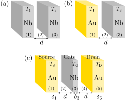
The rest of the paper is organized as follows. In Sec. II we introduce the different systems and devices that we analyze in this work and explain how we model the optical properties of the materials involved in these systems (Nb and Au). In Sec. III we briefly discuss the radiative heat transfer between two parallel plates made of Nb to illustrate the impact of the superconducting phase transition in the heat exchanged via radiation. Then, Sec. IV is devoted to the analysis of the radiative heat rectification in a thermal diode made of Au and Nb parallel plates. In Sec. V we study the operation of a three-body system made of a Nb layer between two Au plates as a near-field thermal transistor. Finally, we summarize our main conclusions in Sec. VI.
II Systems and optical properties
As explained in the introduction, the main goal of this work is to study theoretically the performance of near-field thermal diodes and transistors that make use of superconducting materials. For this purpose, we shall first briefly analyze the impact of the superconducting phase transition in the NFRHT in the case of two Nb parallel plates, see Fig. 1(a), in which we shall consider temperatures below and above the superconducting critical temperature of Nb, K. The near-field diode that we shall investigate is schematically depicted in Fig. 1(b) and it consists of two infinite parallel plates made of Au and Nb separated by a gap of size . Finally, the near-field transistor that we shall analyze in detail is shown in Fig. 1(c). In this case, a Nb layer of thickness , referred to as gate, is placed in the middle of the vacuum gap between two infinite parallel plates made of Au, referred to as source and drain. The temperatures of the source, drain, and gate are denoted by , , and , respectively, and we shall assume that . The distance between the gate and the source and drain is denoted by and we shall consider temperatures around (both above and below) .
The analysis of the radiative heat transfer in all the cases shown in Fig. 1 will be done within the framework of the theory of fluctuational electrodynamics Rytov1953 ; Rytov1989 . In this theory, and within the standard local approximation, the optical properties of the materials are fully determined by their frequency-dependent dielectric functions (we only consider here nonmagnetic materials). In what follow, we shall describe how we model the dielectric functions of the two materials involved in our systems under study, Nb and Au.
The Nb dielectric function is described here following Ref. Zimmermann1991 which, in turn, makes use of Mattis and Bardeen theory for diffusive superconductors of arbitrary purity Mattis1958 . This dielectric function is given by
| (1) |
where is the high frequency limit for the permittivity, is the optical conductivity, is the relaxation time, is the vacuum permittivity, and is the plasma frequency. In the superconducting state, the optical conductivity is given by Zimmermann1991
| (2) |
with
| (5) |
and
| (6) |
where
| (7) |
In these expressions, is the energy of the carriers, is the frequency of electromagnetic waves, is the temperature, and is superconducting gap, whose temperature dependence is approximately described by Carless1983
| (8) |
where is the critical temperature. In the normal state (), the corresponding optical conductivity is given by Zimmermann1991
| (9) |
To describe the Au layers, we use the following Drude-like relative permittivity Chapuis2008
| (10) |
where , and are, respectively, the high frequency limit of dielectric function, plasma frequency, and damping of the free carrier.
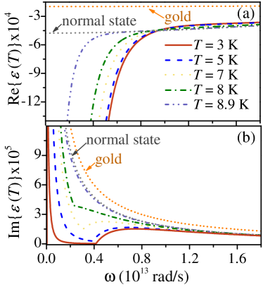
All calculations in this work were performed with the following parameters for Nb: Zimmermann1991 , , K, S/m, and rad/s Kralik2017 . For the Au layers, , rad/s, and rad/s. These parameters are consistent with the experimental ones reported in Ref. Coste2017 for cryogenic temperatures. In Fig. 2 we display the frequency dependence of the real and imaginary part of the dielectric functions of Nb and Au computed with those parameter values. In particular, we show the Nb dielectric function for different temperatures inside the superconducting phase, as well as for temperatures above , i.e., in the normal state.
III Nb parallel plates
Before discussing the functional devices, diode and transistor, it is convenient to analyze the impact of the superconducting phase transition in the NFRHT. For this purpose, we revisit here the case of two Nb parallel plates, see Fig. 1(a), which has been analyzed, both theoretically and experimentally, in Ref. Kralik2017 . Within the theory of fluctuational electrodynamics, the net power per unit area (heat flux) exchanged via radiation by two infinite parallel plates, see Fig. 1(a), is given by Polder1971
| (11) |
where , is the absolute temperature of the layer , is the radiation frequency, is the magnitude of the wave vector parallel to the surface planes, and is the total transmission probability of the electromagnetic propagating () and evanescent () waves, given by
| (14) |
Here, is the the wave vector component perpendicular to the plate surfaces in the vacuum gap and is the velocity of light in vacuum. The reflection amplitudes are given by the Fresnel coefficients
| (15) |
The corresponding linear thermal conductance per unit of area, usually referred to as heat transfer coefficient, is given by
| (16) |
In the case of two black bodies, which is achieved when for all frequencies for propagating waves, this result reduces to the Stefan-Boltzmann law
| (17) |
where is the Stefan-Boltzmann constant (not to be confused with a conductivity).
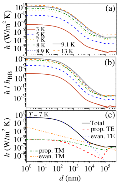
In Fig. 3(a) we show the results for the gap dependence of the heat transfer coefficient of two Nb parallel plates for different temperatures across the superconducting phase transition ( K). One can see that the heat transfer coefficient is greatly enhanced in the near-field regime ( nm) and it saturates for small gaps ( nm). Notice also that there is a pronounced temperature dependence, especially for temperatures below . This strong dependence is due to both the impact of the superconducting phase transition and the fact that the temperature itself is being changed by an amount comparable to its absolute value. To disentangle those two dependencies, it is convenient to normalize the heat transfer coefficient by the corresponding result for two black bodies, as we do in Fig. 3(b). With this normalization, we see that the blackbody limit is greatly overcome in the near-field regime (by almost 5 orders of magnitude at K and gaps nm). More importantly for this work, there is a very strong reduction of the NFRHT upon decreasing the temperature below . For instance, for small gaps the NFRHT for 3 K is about 10 smaller than for K. In simple terms, this dramatic effect can be explained by the presence of a gap in the spectrum of a superconductor that naturally leads to a strong reduction of the emissivity of the material at low frequencies, see Fig. 2(b). On the other hand, and in order to give an insight into the NFRHT in the superconducting phase, we show in Fig. 3(c) the gap dependence of the different contributions to the heat transfer coefficient for the Nb parallel plates for a temperature K, including both propagating and evanescent waves for both TE (or ) and TM (or ) waves. As expected for metals, the NFRHT is largely dominated by evanescent TE modes, which can be attributed to total internal reflection modes as explained in detail in Ref. Chapuis2008 .
IV Near-field thermal rectifier
Now we turn to the analysis of the thermal rectifier shown in Fig. 1(b) and composed by two parallel plates made of Nb and Au. As explained in the introduction, there have been many proposals for near-field thermal rectifiers employing a variety of materials that undergo a phase transition as a function of temperature. In particular, Ordoñez-Miranda et al. Ordonez2017 proposed a diode with terminals made of parallel plates of Nb and SiO2 and operating at temperatures between 1 and 8.7 K, for which Nb is superconducting. These authors reported that the rectification factor (see definition below) could reach 71% for gaps on the order of 60 m. In what follows, we show that the performance of a superconducting near-field thermal rectifier can be boosted by using a metal as a second thermal reservoir instead of a polar dielectric like silica.
The heat flux in an asymmetric system like that of Fig. 1(b) can be calculated with the formulas described in the previous section. For the rectifying behavior, we calculated the net heat flux for both forward (FB) and reverse (RB) bias configuration. The forward (reverse) bias heat flux, (), was calculated by setting K and with ( and K ), i.e., in forward (reverse) bias the temperature gradient is from media (1) to (3) [(3) to (1)]. The rectification factor is defined as
| (18) |
Notice that with this definition, is bounded between 0 and 1.
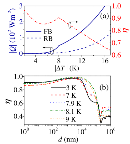
In Fig. 4 we summarize our main results for the thermal diode of Fig. 1(b). In the upper panel we show the forward and reverse bias heat fluxes for nm as a function of the temperature difference , while the temperature of the coldest plate is fixed at 1 K. The corresponding rectification factor is also shown. Notice that very high values above 0.9 can be achieved for small values of the temperature difference. In the lower panel we show the results for the gap dependence of the rectification factor for various temperature differences. As one can see, very high values are reached in the near-field regime in a huge range of gap size values (of about four decades). In particular, values as high as 98.7% are obtained for gaps on the order of 10 m, see Fig. 4(b), which to our knowledge are the highest ever reported and, in particular, are much higher than those predicted in previous proposals of superconducting thermal rectifiers Ordonez2017 .
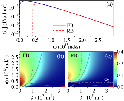
To gain some physical insight into the origin of the huge rectification ratios in our system, we show in Fig. 5(a) the spectral heat flux (or power per unit of area and frequency) as a function of frequency for the forward and reverse bias for a case in which the temperatures of the cold and hot reservoirs are 1 and 8.9 K, respectively. In this case, the gap size is 10 nm. The spectral heat flux has the characteristic form in metallic systems in which the evanescent TE electromagnetic modes completely dominate the NFRHT Chapuis2008 ; Kim2015 , which is also the case in our asymmetric configuration. Notice, in particular, that for the reverse bias there is an abrupt frequency cut-off below which the spectral function drastically drops. For the reverse bias, the Nb plate is at 1 K, i.e., deep into the superconducting phase, and that cut-off simply corresponds to the frequency rad/s that is required to break a Cooper pair. Below this frequency, the emissivity of the Nb plate is drastically reduced due to the presence of a gap in the electronic spectrum, which explains the strong reduction of the radiative heat transfer, as compared to the forward bias configuration. This interpretation is further illustrated in Fig. 5(b,c) where we show the corresponding transmission probability for the evanescent TE modes as a function of the frequency and the parallel component of the wave vector. Notice that for the reverse bias, panel (c), the transmission is very small below . This fact, together with the frequency dependence of the thermal factor , see dotted lines in panels (b) and (c), determining the electromagnetic modes available for heat transfer, see Eq. (11), explains the huge difference between in the net power between the reverse and the forward bias configurations.
V Near-field thermal transistor
Let us now analyze the superconducting thermal transistor depicted in Fig. 1(c) that features a Nb layer of thickness as a gate electrode that is placed at a distance of two Au plates that act as source and drain. To compute the different heat exchanges in this three-body system, we have employed the many-body theory put forward in Ref. Messina2012 . According to this theory, the heat flux received by the drain, , and the heat flux lost by the source, , in the near-field thermal transistor of Fig. 1(c) are given by
| (19) | |||||
| (20) |
where , and is the transmission probability of electromagnetic waves from region to in Fig. 1(c). For a symmetric configuration (source and drain equidistant to gate), as considered in this work, these transmissions probabilities are given by
| (21) |
where
Additionally, the transmission probabilities () can be obtained after substitution and in (). The corresponding net heat flux received or emitted by the gate is defined as Ben-Abdallah2014
| (22) |
and the amplification factor as
| (23) |
where . Amplification requires a negative differential conductance and it is characterized by Ben-Abdallah2014 . In what follows, we shall choose K, K, and .
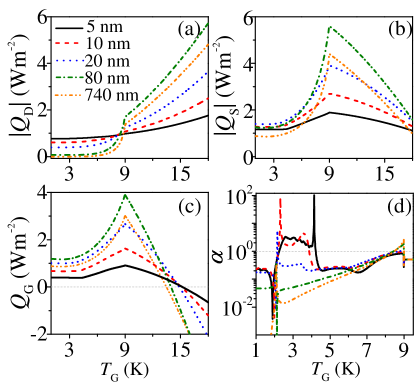
In Fig. 6(a-c) we present the different powers gained or lost by the three thermal reservoirs (drain, source and gate) as a function of the gate temperature for different values of the gate thickness and a Nb-Au gap nm. As expected, the heat received by the drain, , increases monotonically with , irrespective of whether the gate is in the normal or in the superconducting state, see Fig. 6(a). On the other hand, and contrary to what one could naively expect, the heat lost by the source, see panel (b), and the net heat in the gate, see panel (c), do not decrease monotonically upon increasing . This peculiar behavior only takes place in the superconducting state () and it is a necessary condition for the amplification to occur, see Eq. (23). In Fig. 6(d) we show the corresponding value of the amplification factor, defined in Eq. (23), as a function of . Notice that for thin Nb layers, values of larger than 1 are possible in a certain range of temperatures within the superconducting phase, and for very specific values of the amplification factor can reach values close to 100. In those cases, our three-body system truly behaves as a near-field transistor. This is, however, never the case when the Nb gate is in its normal state where tends to .
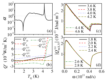
To get some insight into the origin of the amplification, we show in Fig. 7(b) the derivatives of the heat exchanges in the source and drain with respect to the gate temperature, , for the case of nm shown in Fig. 6(d), see also Fig. 7(a). From Eq. (23) we see that amplification () requires that . The dependence with the gate temperature shown in Fig. 7(b) explains why there is amplification in the range between approximately 2.5 and 4.2 K and why there is a huge peak at around 4.2 K, which corresponds to the situation in which . Moreover, we show in Fig. 7(b) the different individual contributions to following Eq. (20). There we see that the key temperature dependence of is mainly determined by the term involving for TE (or ) polarization, which is related to the heat lost by the source to the combined gate-drain system. To understand the -dependence of this term, we illustrate in Fig. 7(c) the evolution with the gate temperature of the corresponding spectral contribution. As one can see, the temperature dependence is only significant in the frequency region close to for the temperatures in which the amplification occurs. As we show in Fig. 7(d), that temperature dependence is much weaker when the gate thickness is increased, which explains why the amplification gets lost as the gate thickness increases.
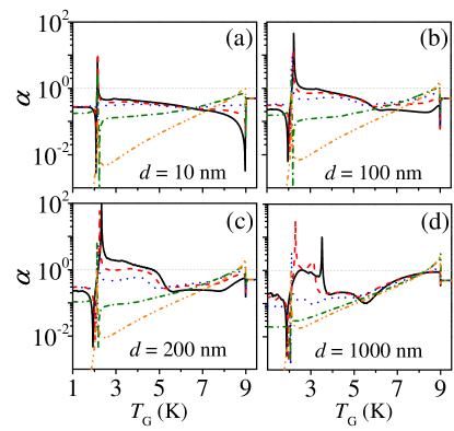
For completeness, we have systematically explored the role of the gap size between the Nb gate and the Au reservoirs. We show a summary of these results in Fig. 8 where we show the amplification factor as a function of the gate temperature for different values of (and also different values of the gate thickness). As one can see, the optimal amplification occurs for gap sizes on the order of a few hundred nm, while it only appears at some special points of the parameter space for smaller and larger gap values. In all cases, the amplification only appears for very thin Nb films.
VI Conclusions
Motivated by recent theoretical proposals and experiments on the use of phase-transition materials to realize near-field thermal devices that mimic electronic components, we have presented in this work a theoretical study of the performance of near-field thermal diodes and transistors based on the combination of superconductors and normal metals. We have shown that the drastic reduction in the thermal emission of a metal when it undergoes a superconducting transition can be utilized to realize heat rectification in two-body systems and heat amplification in three-body devices. In particular, we have shown that a system formed by two parallel plates made of Au and (superconducting) Nb can act as a near-field thermal diode that exhibits striking rectification ratios very close to unity in a wide range of gap size values, outperforming all the existent proposals to date. Moreover, we have shown that a Nb layer placed in the middle of two Au plates can amplify the heat transferred to the drain at temperatures below Nb critical temperature. The ideas put forward in this work can be extended to propose other functional devices such as thermal logic gates and, overall, it illustrates the potential of the use of superconducting materials for near-field thermal management at low temperatures.
Acknowledgements.
J.C.C. acknowledges funding from the Spanish Ministry of Economy and Competitiveness (MINECO) (contract No. FIS2017-84057-P).References
- (1) B. Song, A. Fiorino, E. Meyhofer, and P. Reddy, Near-field radiative thermal transport: From theory to experiment, AIP Advances 5, 053503 (2015).
- (2) J. C. Cuevas and F. J. García-Vidal, Radiative heat transfer, ACS Photonics 5, 3896 (2018).
- (3) S.-A. Biehs, R. Messina, P. S. Venkataram, A. W. Rodriguez, J. C. Cuevas, P. Ben-Abdallah, Near-field radiative heat transfer in many-body systems, arXiv:2007.05604.
- (4) D. Polder and M. Van Hove, Theory of radiative heat transfer between closely spaced bodies Phys. Rev. B 4, 3303 (1971).
- (5) S. M. Rytov, Theory of Electric Fluctuations and Thermal Radiation, (Air Force Cambridge Research Center, Bedford, MA, 1953).
- (6) S. M. Rytov, Y. A. Kravtsov, and V. I. Tatarskii, Principles of Statistical Radiophysics, Vol. 3 (Springer-Verlag, Berlin Heidelberg, 1989).
- (7) A. Kittel, W. Müller-Hirsch, J. Parisi, S.-A. Biehs, D. Reddig, and M. Holthaus, Near-Field Heat Transfer in a Scanning Thermal Microscope, Phys. Rev. Lett. 95, 224301 (2005).
- (8) A. Narayanaswamy, S. Shen, and G. Chen, Near-field radiative heat transfer between a sphere and a substrate, Phys. Rev. B 78, 115303 (2008).
- (9) L. Hu, A. Narayanaswamy, X. Y. Chen, and G. Chen, Near-field thermal radiation between two closely spaced glass plates exceeding Planck’s blackbody radiation law, Appl. Phys. Lett. 92, 133106 (2008).
- (10) E. Rousseau, A. Siria, G. Jourdan, S. Volz, F. Comin, J. Chevrier, and J.-J, Greffet, Radiative heat transfer at the nanoscale, Nat. Photonics 3, 514 (2009).
- (11) S. Shen, A. Narayanaswamy, and G. Chen, Surface phonon polaritons mediated energy transfer between nanoscale gaps, Nano Lett. 9, 2909 (2009).
- (12) R. S. Ottens, V. Quetschke, S. Wise, A. A. Alemi, R. Lundock, G. Mueller, D. H. Reitze, D. B. Tanner, and B. F. Whiting, Near- Field Radiative Heat Transfer Between Macroscopic Planar Surfaces, Phys. Rev. Lett. 107, 014301 (2011).
- (13) S. Shen, A. Mavrokefalos, P. Sambegoro, and G. Chen, Nanoscale thermal radiation between two gold surfaces, Appl. Phys. Lett. 100, 233114 (2012).
- (14) T. Kralik, P. Hanzelka, M. Zobac, V. Musilova, T. Fort, and M. Horak, Strong Near-Field Enhancement of Radiative Heat Transfer Between Metallic Surfaces, Phys. Rev. Lett. 109, 224302 (2012).
- (15) P. J. van Zwol, L. Ranno, and J. Chevrier, Tuning Near Field Radiative Heat Flux Through Surface Excitations with a Metal Insulator Transition, Phys. Rev. Lett. 108, 234301 (2012).
- (16) P. J. van Zwol, S. Thiele, C. Berger, W. A. de Heer, and J. Chevrier, Nanoscale Radiative Heat Flow Due to Surface Plasmons in Graphene and Doped Silicon, Phys. Rev. Lett. 109, 264301 (2012).
- (17) B. Guha, C. Otey, C. B. Poitras, S. H. Fan, and M. Lipson, Near-field radiative cooling of nanostructures, Nano Lett. 12, 4546 (2012).
- (18) J. Shi, P. Li, B. Liu, and S. Shen, Tuning near field radiation by doped silicon, Appl. Phys. Lett. 102, 183114 (2013).
- (19) L. Worbes, D. Hellmann, and A. Kittel, Enhanced Near-Field Heat Flow of a Monolayer Dielectric Island, Phys. Rev. Lett. 110, 134302 (2013).
- (20) R. St-Gelais, B. Guha, L. X. Zhu, S. H. Fan, and M. Lipson, Demonstration of strong near-field radiative heat transfer between integrated nanostructures, Nano Lett. 14, 6971 (2014).
- (21) B. Song, Y. Ganjeh, S. Sadat, D. Thompson, A. Fiorino, V. Fernández-Hurtado, J. Feist, F. J. Garcia-Vidal, J. C. Cuevas, P. Reddy, and E. Meyhofer, Enhancement of near-field radiative heat transfer using polar dielectric thin films, Nat. Nanotechnol. 10, 253 (2015).
- (22) K. Kim, B. Song, V. Fernández-Hurtado, W. Lee, W. Jeong, L. Cui, D. Thompson, J. Feist, M. T. H. Reid, F. J. García-Vidal, J. C. Cuevas, E. Meyhofer, P. Reddy, Radiative heat transfer in the extreme near field, Nature (London) 528, 387 (2015).
- (23) M. Lim, S. S. Lee, and B. J. Lee, Near-field thermal radiation between doped silicon plates at nanoscale gaps, Phys. Rev. B 91, 195136 (2015).
- (24) R. St-Gelais, L. Zhu, S. Fan, and M. Lipson, Near-field radiative heat transfer between parallel structures in the deep subwavelength regime, Nat. Nanotechnol. 11, 515 (2016).
- (25) B. Song, D. Thompson, A. Fiorino, Y. Ganjeh, P. Reddy, E. Meyhofer, Radiative heat conductances between dielectric and metallic parallel plates with nanoscale gaps, Nat. Nanotechnol. 11, 509 (2016).
- (26) M. P. Bernardi, D. Milovich, M. Francoeur, Radiative heat transfer exceeding the blackbody limit between macroscale planar surfaces separated by a nanosize vacuum gap, Nat. Commun. 7, 12900 (2016).
- (27) L. Cui, W. Jeong, V. Fernández-Hurtado, J. Feist, F. J. García-Vidal, J. C. Cuevas, E. Meyhofer, P. Reddy, Study of radiative heat transfer in Ångström- and nanometre-sized gaps, Nat. Commun. 8, 14479 (2017).
- (28) K. Kloppstech, N. Könne, S.-A. Biehs, A. W. Rodriguez, L. Worbes, D. Hellmann, A. Kittel, Giant heat transfer in the crossover regime between conduction and radiation, Nat. Commun. 8, 14475 (2018).
- (29) M. Ghashami, H. Geng, T. Kim, N. Iacopino, S.-K. Cho, K. Park, Precision Measurement of Phonon-Polaritonic Near-Field Energy Transfer Between Macroscale Planar Structures Under Large Thermal Gradients, Phys. Rev. Lett. 120, 175901 (2018).
- (30) A. Fiorino, D. Thompson, L. Zhu, B. Song, P. Reddy, E. Meyhofer, Giant enhancement in radiative heat transfer in sub-30 nm gaps of plane parallel surfaces, Nano Lett. 18, 3711 (2018).
- (31) J. DeSutter, L. Tang, and M. Francoeur, A near-field radiative heat transfer device, Nat. Nanotechnol. 14, 751 (2019).
- (32) C. Otey, W. T. Lau, and S. Fan, Thermal Rectification through Vacuum. Phys. Rev. Lett. 104, 154301 (2010).
- (33) S. Basu and M. Francoeur, Near-field radiative transfer based thermal rectification using doped silicon. Appl. Phys. Lett. 98, 113106 (2011).
- (34) H. Iizuka, and S. H. Fan, Rectification of evanescent heat transfer between dielectric-coated and uncoated silicon carbide plates, J. Appl. Phys. 112, 024304 (2012).
- (35) L. P. Wang and Z. M. Zhang, Thermal rectification enabled by near-field radiative heat transfer between intrinsic silicon and a dissimilar material, Nanoscale Microscale Thermophys. Eng. 17, 337 (2013).
- (36) P. Ben-Abdallah and S. A. Biehs, Phase-change radiative thermal diode, Appl. Phys. Lett. 103, 191907 (2013).
- (37) Y. Yang, S. Basu, and L. P. Wang, Radiation-based near-field thermal rectification with phase transition materials, Appl. Phys. Lett. 103, 163101 (2013).
- (38) J. G. Huang, Q. Li, Z. H. Zheng, Y. M. Xuan, Thermal rectification based on thermochromic materials, Int. J. Heat Mass Transfer 67, 575 (2013).
- (39) E. Nefzaoui, K. Joulain, J. Drevillon, Y. Ezzahri, Radiative thermal rectification using superconducting materials, Appl. Phys. Lett. 104, 103905 (2014).
- (40) Y. Yang, S. Basu, L. P. Wang, Vacuum thermal switch made of phase transition materials considering thin film and substrate effects, J. Quant. Spectrosc. Radiat. Transfer 158, 69 (2015).
- (41) A. Ghanekar, J. Ji, Y. Zheng, High-rectification near-field thermal diode using phase change periodic nanostructure, Appl. Phys. Lett. 109, 123106 (2016).
- (42) Z. H. Zheng, X. L. Liu, A. Wang, Y. M. Xuan, Graphene-assisted near-field radiative thermal rectifier based on phase transition of vanadium dioxide (VO2), Int. J. Heat Mass Transfer 109, 63 (2017).
- (43) P. J. van Zwol, K. Joulain, P. Ben-Abdallah, J. Chevrier, Phonon Polaritons enhance near-field thermal transfer across the phase transition of VO2, Phys. Rev. B 84, 161413 (2011).
- (44) P. J. van Zwol, K. Joulain, P. Ben-Abdallah, J. J. Greffet, J. Chevrier, Fast nanoscale heat-flux modulation with phase-change materials, Phys. Rev. B 83, 201404 (2011).
- (45) K. Ito, K. Nishikawa, A. Miura, H. Toshiyoshi, H. Iizuka, Dynamic modulation of radiative heat transfer beyond the blackbody limit, Nano Lett. 17, 4347 (2017).
- (46) K. Ito, K. Nishikawa, A. Miura, H. Toshiyoshi, Experimental investigation of radiative thermal rectifier using vanadium dioxide, Appl. Phys. Lett. 105, 253503 (2014).
- (47) A. Fiorino, D. Thompson, L. Zhu, R. Mittapally, S.-A. Biehs, O. Bezencenet, N. El-Bondry, S. Bansropun, P. Ben-Abdallah, E. Meyhofer, P. Reddy, A thermal diode based on nanoscale thermal radiation, ACS Nano 12, 5774 (2018).
- (48) A. Ghanekar, Y. Tian, M. Ricci, S. Zhang, O. Gregory, and Y. Zheng, Near-field thermal rectification devices using phase change periodic nanostructure, Opt. Express 26, A209 (2018).
- (49) P. Ben-Abdallah and S.-A. Biehs, Near-field Thermal Transistor, Phys. Rev. Lett. 112, 044301 (2014).
- (50) R. Messina, M. Antezza, and P. Ben-Abdallah, Three-body Amplification of Photon Heat Tunneling, Phys. Rev. Lett. 109, 244302 (2012).
- (51) V. Kubytskyi, S. A.Biehs, and P. Ben-Abdallah, Radiative Bistability and Thermal Memory, Phys. Rev. Lett. 113, 074301 (2014).
- (52) P. Ben-Abdallah and S. A. Biehs, Towards Boolean operations with thermal photons. Phys. Rev. B 94, 241401 (2016).
- (53) P. Ben-Abdallah and S. A. Biehs, Thermotronics: Towards nanocircuits to manage radiative heat flux, Zeitschrift für Naturforschung A 72, 151 (2017)
- (54) T. Kralik, V. Musilova, T. Fort, and A. Srnka, Effect of superconductivity on near-field radiative heat transfer, Phys. Rev. B 95, 060503(R) (2017).
- (55) V. Musilová, T. Králík, T. Fot, and M. Macek, Strong suppression of near-field radiative heat transfer by superconductivity in NbN, Phys. Rev. B 99, 024511 (2019).
- (56) S. G. Castillo-López, G. Pirruccio, C. Villarreal, and R. Esquivel‑Sirvent, Near‑field radiative heat transfer between high‑temperature superconductors, Sci. Rep. 10, 16066 (2020).
- (57) J. O. Ordoñez-Miranda, K. Joulain, D. De Sousa M., Y. Ezzahri and J. Drevillon, Photonic thermal diode based on superconductor, J. Appl. Phys. 122, 093105 (2017).
- (58) W. Zimmermann, E. H. Brandt, M. Bauer, E. Seider, and L. Genzel, Optical conductivity of BCS superconductors with arbitrary purity, Physica C 183, 99 (1991).
- (59) D. C. Mattis and J. Bardeen, Theory of the Anomalous Skin Effect in Normal and Superconducting Metals, Phys. Rev. 111, 412 (1958).
- (60) D.C. Carless, H.E. Hall and J.R. Hook, Vibrating wire measurements in liquid 3He II. The superfluid B phase, J. Low Temp.Phys. 50, 605 (1983).
- (61) P. O. Chapuis, S. Volz, C. Henkel, K. Joulain, and J. J. Greffet, Effects of spatial dispersion in near-field radiative heat transfer between two parallel metallic surfaces, Phys. Rev. B 77, 035431 (2008).
- (62) A. Coste, F. Eloi, C. Arnold, G. Colas des Francs, X. Quélin, S. Buil, A. Bouhelier, J. C. Weeber, M. Nasilowski, B. Dubertret, and J.-P. Hermier, Significant decrease of the optical losses in the coupling between colloidal CdSe/CdS nanocrystals and a flat gold film at cryogenic temperature, Phys. Rev. B 96, 195416 (2017).