Topological insulator nanoribbon Josephson junctions: evidence for size effect in transport properties
Abstract
- Abstract
-
We have used Bi2Se3 nanoribbons, grown by catalyst-free Physical Vapor Deposition to fabricate high quality Josephson junctions with Al superconducting electrodes. In our devices we observe a pronounced reduction of the Josephson critical current density by reducing the width of the junction, which in our case corresponds to the width of the nanoribbon. Because the topological surface states extend over the entire circumference of the nanoribbon, the superconducting transport associated to them is carried by modes on both the top and bottom surfaces of the nanoribbon. We show that the reduction as a function of the nanoribbons width can be accounted for by assuming that only the modes travelling on the top surface contribute to the Josephson transport as we derive by geometrical consideration. This finding is of a great relevance for topological quantum circuitry schemes, since it indicates that the Josephson current is mainly carried by the topological surface states.
I Introduction
The study of the proximity effect between a superconductor and a semiconductor or an unconventional metal, has lately received a dramatic boost due to the increasing possibilities to manufacture a larger variety of interfaces and materials. Novel phenomenology of the proximity effect is currently coming from the integration of semiconducting nanowires, with strong spin orbit coupling, as barriers, as well as the edge and surface states of two-dimensional (2D) and three-dimensional (3D) Topological Insulators (TIs) [1, 2, 3, 4, 5], and Dirac semimetals [6, 7]. In these cases, the Josephson transport properties of the hybrid devices would manifest neat fingerprints related to the formation of Majorana bound states, of great interest for topological quantum computation [8, 9, 10]. Lately Superconductor-TI-Superconductor Josephson junctions with 2D [11] and 3D TIs have shown a 4 periodic Josephson current phase relations [12, 13, 14] which could be associated to the presence of Majorana modes [15] and a gate-tunable Josephson effects [16, 17, 2, 18, 19] when the TI is tuned through the TI’s Dirac point. Still several aspects of the physics of the Josephson effect related to the topological protected edge/surface states and the contribution of the unavoidable bulk remain to be clarified. In this respect the use of 3D TI nanoribbons could be advantageous because of the reduced number of transport channels involved in the transport. Here the transport is ruled by the quantization of the nanoribbon’s propagation modes, which could give new hints about the Josephson phenomenology associated to the Topological Surface States (TSS).
In this work, we have fabricated Josephson junctions by using Bi2Se3 Topological Insulator Nanoribbons (TINR) with a widths spanning from 50 nm to almost a micron. Because the TSS extend over the entire circumference of the TINR, the superconducting transport associated to them is carried by modes on both the top and bottom surface of the nanoribbon. As shown in Fig. 1a, in our TINR Josephson junction the current flows between the superconducting contacts fabricated on the top surface of the nanoribbon. For the TINR with a circumference = 2 + 2 (where is the width and the thickness of the nanoribbon) the transverse momentum , perpendicular to the current (see Fig. 1), is quantized as:
| (1) |
where is an integer [21]. Therefore, the modes with 0 remain on the top surface while the modes with 0 are winding around the perimeter of the TINR (see Fig. 1a). Here we show that the value of the Josephson current density strongly depends on the junction width, that in our case corresponds to the width of the nanoribbons (Fig. 1a). We discuss the possible origin of this phenomenology also in connection with the fact that only small value modes are involved in the Josephson transport, that are the ones which travel on the top surface of the nanoribbon. This number reduces by reducing the nanoribbon width (see Eq. 1). This finding is of a great relevance since it indicates that a) the Josephson current is mainly carried by the surface states and b) because of the selectivity in , the number of modes involved in the transport scales much faster compared to the width. This is of great relevance for topological quantum circuitry schemes.
II Experimental details and results
Nanoribbons of Bi2Se3 with a variation of widths from 50 nm to about 1 m were grown as reported in ref.[22]. For the fabrication of Josephson junctions, nanoribbons were transferred to pre-patterned substrates of Si/300 nm SiO2 and SrTiO3 (STO). We used two different TINR growth batches for the two substrates, respectively. For the two batches the carrier densities of the topological surface states measured through Shubnikov de Haas oscillations varied by a factor of 2 [22]. A standard process of electron beam lithography was used, followed by the evaporation of 3 and 80 nm thick layers of Pt and Al respectively. Before the evaporation of the metals, the samples were etched for 30 s by Ar ion milling to remove the native oxide layer of the nanoribbons. SEM images of the fabricated Al/Bi2Se3/Al Josephson junctions for different nanoribbon widths are shown in Fig. 1b,c. The Pt interlayer between the Bi2Se3 and Al has an important role in forming of transparent interface, as it was shown in our previous works [23, 24, 3].
Junctions were measured at a base temperature of 19 mK, in an -filtered dilution refrigerator.

Planar Josephson junction can be described as SIS′I′-N-I′S′IS. Here S′ is the proximized TINR which lies underneath the superconductor (S) - Al, and N represents the not-covered TINR part between the two Al electrodes (see schematics in the inset of Fig. 1b). I is the interface of the barrier between the Al and the Bi2Se3 nanoribbon, while I′ represents the barrier interface formed between the Bi2Se3 under the Al and that Bi2Se3 of the normal metal region N (nanogap). We have previously demonstrated that both I and I′ are highly transparent [23, 3] and that we have full control of the strength and phenomenology of the proximity effect. When the voltage drop across the Al/Bi2Se3 interface is negligible, compared to that across the TI in the nanogap, as in our case [25], the physics of the planar junction is effectively that of a S′I′-N-I′S′.

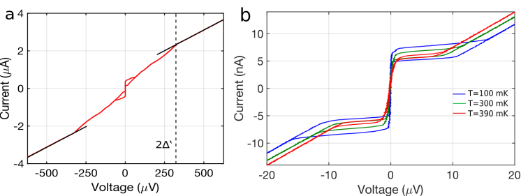
A typical current-voltage characteristic (IVC) of one of the TINR based Josephson junctions is shown in Fig. 2a. The IVCs of our junctions have a hysteresis which points to an increased electron temperature as the junction is switched to the resistive state [26]. A clear gap structure is seen at 2 (where is the induced gap of the order of 170V); several bumps in the IVC at 2 are also visible: as we have previously demonstrated they are connected to multiple Andreev reflections that are made possible by the high transparency of the I and I′ barriers [23]. The IVCs measured at various temperatures are shown in Fig. 2b. At higher temperatures we observe a finite resistance in the supercurrent branch. This could be attributed to premature switching and consecutive retrapping of the superconducting phase difference [27, 28, 29, 30]. The so-called phase diffusion regime is characteristic for moderate to low quality factor Josephson junction. The quality factor can be estimated using , with the plasma frequency , where is the superconductive flux quantum, and is the real part of the shunting admittance of a dc biased Josephson junction [31, 32]. Here the capacitance is dominated by the shunting capacitance through the substrate.

For STO with a relative dielectric contant of 25000 at low temperatures we approximate pF resulting in a quality factor smaller than one for junctions having a critical current lower than 50 nA. Instead for the Si/SiO2 substrate it is more difficult to estimate the shunting capacitance due to the conducting substrate. However we expect a much smaller capacitance value resulting in quality factors smaller than one for critical currents already below 500 nA.

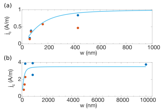
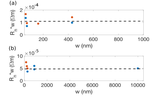
The value of the critical current of the junction is obtained from the forward scan, and the critical current density is calculated accordingly by dividing by the width of the nanoribbon . The normal state resistance is determined by the inverse of the slope, calculated from the IVC region at voltages above 2 in S′ (represented by the area of Bi2Se3 underneath the Al). Fig. 3a,b show the dependence of the as a function of the for devices with different lengths fabricated on Si/SiO2 and STO substrates, respectively. In Fig. 3b we have included a m wide junction where the Al electrodes are pattered along the length of TINR; for this device no winding modes are expected to contribute to the Josephson transport. One clearly sees that if the length is fixed the sharply decreases as a function of the width of the nanoribbon. We note that the value of can change by a factor of 5-6 by going from the narrowest nanoribbons of 60 nm to the widest ones. In contrast, as shown in Fig. 4a,b, the specific resistance, obtained by considering the product for the devices on the Si/SiO2 and STO substrate, respectively, is almost independent of . This fact allows to exclude that the reduction of the at small widths has its origin in strong modifications/deterioration of the junction specific resistance for narrow TINR.
III Discussion and conclusions
What is the origin of this peculiar () phenomenology? As we have discussed earlier, the explanation of the phenomenon can have its grounds in the quantization of the nanoribon’s propagation modes.
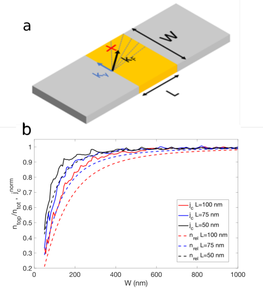
One can derive that the relative number of modes ntop/ntot travelling only on the top surface reduces with the junction width for a fixed junction length . Here is the total number of modes:
| (2) |
and is the number of modes travelling only on the top surface of the nanoribbon:
| (3) |
The relations above can be obtained from geometric considerations, see Fig. 5a. Here is the Fermi vector.
In Fig. 5b we show the width dependence of the relative number of modes / for three different junction lengths. The curves of Fig. 5b have been obtained by considering = 0.55 nm-1, a value which is typical for our nanoribbons [20]. For = 100 nm we obtain a reduction of the relative number of modes travelling only on the top surface by a factor of 5 when reducing the junction width going from 900 nm to 50 nm.

For comparison in Fig. 5 we also show the full calculation of the supercurrent density following ref. [7] taking into consideration also the angle dependence of the transmission coefficients of each transport mode traveling only on the top surface. We see that the full calculation of and the relative number of transport modes using equation 2 and 3 give the same qualitative behaviour.
This dependency qualitatively reproduces the measured width dependence shown in Fig. 3 a,b. Indeed, the solid lines represent the relative number of transport modes for nm. This suggests that only the modes travelling on the top surface contribute to the Josephson current. We note that critical current density of the 10 m wide device is in agreement with the saturation value of the expected current density, where the contribution of winding modes to the total Josephson current is negligible.
A possible explanation for this finding could be related to the lower mobility of the Dirac states at the interface between the TINR and the substrate. Indeed, our magnetotransport measurements have shown the formation of a trivial 2D gas at the interface with the substrate overlapping with the Dirac states at the nanoribbon bottom (see inset Fig. 1b) [20]. This interaction, which leads to a lower mobility (diffusive transport regime) of the Dirac states, might be responsible for the transport modes winding around the nanoribbon (high modes) contributing less to the Josephson transport. Although we can not exclude that the transport through the trivial 2D gas contributes to the Josephson current it would only cause a constant offset of the values without affecting the overall width dependence. We observe that the overall values of for the devices on the STO substrate are higher than those on Si/SiO2. This can be partially attributed to the larger values of the top surface Dirac carrier density of the batch used to realize the devices on the STO substrate. The larger value of the trivial 2D carrier density we typically observe in devices fabricated on STO substrates [33] could be further responsible for the difference observed in the critical current densities between devices on STO and Si/SiO2 substrates.
To conclude we have fabricated high transparency 3D TINR Josephson junctions showing a peculiar phenomenology that can be associated to the transport through the topological surface states. This is a step forward towards the study of topological superconductivity in few modes devices instrumental for topological quantum computation.
Acknowledgements
This work has been supported by the European Union’s Horizon 2020 research and innovation programme (grant agreement No. 766714/HiTIMe) and by the European Union’s project NANOCOHYBRI (Cost Action CA 16218). G.K. acknowledges European Regional Development Fund project No 1.1.1.2/VIAA/1/16/198. This work was supported by the European Union H2020 under the Marie Curie Actions (766025-QuESTech).
Data availability
The data that support the findings of this study are available from the corresponding author upon reasonable request.
References
- [1] J. Hajer, M. Kessel, C. Brüne, M. P. Stehno, H. Buhmann, and L. W. Molenkamp, “Proximity-Induced Superconductivity in CdTe–HgTe Core–Shell Nanowires”, Nano Letters 19, 4078-4082 (2019).
- [2] L. A. Jauregui, M. Kayyalha, A. Kazakov, I. Miotkowski, L. P. Rokhinson, and Y. P. Chen, “Gate-tunable supercurrent and multiple Andreev reflections in a superconductor - topological insulator nanoribbon-superconductor hybrid device”, Applied Physics Letters 112, 093105-4 (2018).
- [3] S. Charpentier, L. Galletti, G. Kunakova, R. Arpaia, Y. Song, R. Baghdadi, S. M. Wang, A. Kalaboukhov, E. Olsson, F. Tafuri, D. Golubev, J. Linder, T. Bauch, and F. Lombardi, “Induced unconventional superconductivity on the surface states of Bi2Te3 topological insulator”, Nature Communications 8, 2019 (2017).
- [4] L. Galletti, S. Charpentier, M. Iavarone, P. Lucignano, D. Massarotti, R. Arpaia, Y. Suzuki, K. Kadowaki, T. Bauch, A. Tagliacozzo, F. Tafuri, and F. Lombardi, “Influence of topological edge states on the properties of Al/Bi2Se3/Al hybrid Josephson devices”, Physical Review B - Condensed Matter and Materials Physics 89, 134512-9 (2014).
- [5] V. S. Stolyarov, D. S. Yakovlev, S. N. Kozlov, O. V. Skryabina, D. S. Lvov, A. I. Gumarov, O. V. Emelyanova, P. S. Dzhumaev, I. V. Shchetinin, R. A. Hovhannisyan, S. V. Egorov, A. M. Kokotin, W. V. Pogosov, V. V. Ryazanov, M. Y. Kupriyanov, A. A. Golubov, and D. Roditchev, “Josephson current mediated by ballistic topological states in Bi2Te2.3Se0.7 single nanocrystals”, Communications Materials 1, 38 (2020).
- [6] C. Z. Li, C. Li, L. X. Wang, S. Wang, Z. M. Liao, A. Brinkman, and D. P. Yu, “Bulk and surface states carried supercurrent in ballistic Nb-Dirac semimetal Cd3As2 nanowire-Nb junctions”, Physical Review B 97, 115446-8 (2018).
- [7] C. Li, J. C. de Boer, B. de Ronde, S. V. Ramankutty, E. van Heumen, Y. Huang, A. de Visser, A. A. Golubov, M. S. Golden, and A. Brinkman, “4-periodic Andreev bound states in a Dirac semimetal”, Nature Materials 17, 875-880 (2018).
- [8] L. Fu and C. L. Kane, “Superconducting proximity effect and majorana fermions at the surface of a topological insulator”, Physical Review Letters 100, 096407 (2008).
- [9] C. Nayak, S. H. Simon, A. Stern, M. Freedman, and S. Das Sarma, “Non-Abelian anyons and topological quantum computation”, Reviews of Modern Physics 80, 1083-1159 (2008).
- [10] G.-Y. Huang and H. Q. Xu, “Majorana fermions in topological-insulator nanowires : From single superconducting nanowires to Josephson junctions”, Physical Review B - Condensed Matter and Materials Physics 95, 155420-6 (2017).
- [11] J. Wiedenmann, E. Bocquillon, R. S. Deacon, S. Hartinger, O. Herrmann, T. M. Klapwijk, L. Maier, C. Ames, C. Brune, C. Gould, A. Oiwa, K. Ishibashi, S. Tarucha, H. Buhmann, and L. W. Molenkamp, “4-periodic Josephson supercurrent in HgTe-based topological Josephson junctions”, Nature Communications 7, 10303 (2016).
- [12] L. P. Rokhinson, X. Liu, and J. K. Furdyna, “The fractional a.c. Josephson effect in a semiconductor-superconductor nanowire as a signature of Majorana particles”, Nature Physics 8, 795-799 (2012).
- [13] K. L. Calvez, L. Veyrat, F. Gay, P. Plaindoux, C. Winkelmann, H. Courtois, and B. Sacépé, “Joule overheating poisons the fractional ac Josephson effect in topological Josephson junctions”, Communications Physics , 1-9 (2018).
- [14] P. Schüffelgen, D. Rosenbach, C. Li, T. W. Schmitt, M. Schleenvoigt, A. R. Jalil, S. Schmitt, J. Kölzer, M. Wang, B. Bennemann, U. Parlak, L. Kibkalo, S. Trellenkamp, T. Grap, D. Meertens, M. Luysberg, G. Mussler, E. Berenschot, N. Tas, A. A. Golubov, A. Brinkman, T. Schäpers, and D. Grützmacher, “Selective area growth and stencil lithography for in situ fabricated quantum devices”, Nature Nanotechnology 14, 825-831 (2019).
- [15] F. Domínguez, F. Hassler, and G. Platero, “Dynamical detection of Majorana fermions in current-biased nanowires”, Physical Review B - Condensed Matter and Materials Physics 86, 140503-5 (2012).
- [16] M. P. Stehno, P. Ngabonziza, H. Myoren, and A. Brinkman, “Josephson Effect and Charge Distribution in Thin Bi2Te3 Topological Insulators”, Advanced Materials 32, 1908351-6 (2019).
- [17] S. Ghatak, O. Breunig, F. Yang, Z. Wang, A. A. Taskin, and Y. Ando, “Anomalous Fraunhofer Patterns in Gated Josephson Junctions Based on the Bulk-Insulating Topological Insulator BiSbTeSe2”, Nano Letters 18, 5124-5131 (2018).
- [18] M. Kayyalha, M. Kargarian, A. Kazakov, I. Miotkowski, V. M. Galitski, V. M. Yakovenko, L. P. Rokhinson, and Y. P. Chen, “Anomalous low-temperature enhancement of supercurrent in topological insulator nanoribbon Josephson junctions: evidence for low energy Andreev bound states”, Physical Review Letters 122, 047003-6 (2017).
- [19] S. Cho, B. Dellabetta, A. Yang, J. Schneeloch, Z. Xu, T. Valla, G. Gu, M. J. Gilbert, and N. Mason, “Symmetry protected Josephson supercurrents in three-dimensional topological insulators”, Nature Communications 4, 1686-1689 (2013).
- [20] G. Kunakova, L. Galletti, S. Charpentier, J. Andzane, D. Erts, F. Léonard, C. D. Spataru, T. Bauch, and F. Lombardi, “Bulk-Free Topological Insulator Bi2Se3 nanoribbons with Magnetotransport Signatures of Dirac Surface States”, Nanoscale 10, 19595-19602 (2018).
- [21] L. A. Jauregui, M. T. Pettes, L. P. Rokhinson, L. Shi, and Y. P. Chen, “Magnetic field induced helical mode and topological transitions in a topological insulator nanoribbon”, Nature Nanotechnology 11, 345-351 (2016).
- [22] J. Andzane, G. Kunakova, S. Charpentier, V. Hrkac, L. Kienle, M. Baitimirova, T. Bauch, F. Lombardi, and D. Erts, “Catalyst-free vapour-solid technique for deposition of Bi2Te3 and Bi2Se3 nanowires/nanobelts with topological insulator properties”, Nanoscale 7, 15935-15944 (2015).
- [23] G. Kunakova, T. Bauch, E. Trabaldo, J. Andzane, D. Erts, and F. Lombardi, “High transparency Bi2Se3 topological insulator nanoribbon Josephson junctions with low resistive noise properties”, Applied Physics Letters 115, 172601-5 (2019).
- [24] L. Galletti, S. Charpentier, Y. Song, D. Golubev, S. M. Wang, T. Bauch, and F. Lombardi, “High-Transparency Al/Bi2Te3 Double-Barrier Heterostructures”, IEEE Transactions on Applied Superconductivity 27, 1800404-4 (2017).
- [25] B. Aminov, A. Golubov, and M. Y. Kupriyanov, “Quasiparticle current in ballistic constrictions with finite transparencies of interfaces”, Physical Review B - Condensed Matter and Materials Physics 53, 365-373 (1996).
- [26] H. Courtois, M. Meschke, J. T. Peltonen, and J. P. Pekola, “Origin of hysteresis in a proximity josephson junction”, Physical Review Letters 101, 067002-4 (2008).
- [27] V. M. Krasnov, T. Bauch, S. Intiso, E. Hürfeld, T. Akazaki, H. Takayanagi, and P. Delsing, “Collapse of thermal activation in moderately damped josephson junctions”, Phys. Rev. Lett. 95, 157002 (2005).
- [28] J. M. Kivioja, T. E. Nieminen, J. Claudon, O. Buisson, F. W. J. Hekking, and J. P. Pekola, “Observation of transition from escape dynamics to underdamped phase diffusion in a josephson junction”, Phys. Rev. Lett. 94, 247002 (2005).
- [29] D. Massarotti, D. Stornaiuolo, P. Lucignano, L. Galletti, D. Born, G. Rotoli, F. Lombardi, L. Longobardi, A. Tagliacozzo, and F. Tafuri, “Breakdown of the escape dynamics in josephson junctions”, Phys. Rev. B 92, 054501 (2015).
- [30] L. Longobardi, D. Massarotti, D. Stornaiuolo, L. Galletti, G. Rotoli, F. Lombardi, and F. Tafuri, “Direct transition from quantum escape to a phase diffusion regime in YBaCuO biepitaxial josephson junctions”, Physical Review Letters 109, 050601-5 (2012).
- [31] T. Bauch, F. Lombardi, F. Tafuri, A. Barone, G. Rotoli, P. Delsing, and T. Claeson, “Macroscopic Quantum Tunneling in d-wave YBa2Cu3O7-δ Josephson Junctions”, Phys. Rev. Lett. 94, 087003 (2005).
- [32] T. Bauch, T. Lindström, F. Tafuri, G. Rotoli, P. Delsing, T. Claeson, and F. Lombardi, “Quantum dynamics of a d-wave josephson junction”, Science 311, 57-60 (2006).
- [33] G. Kunakova, T. Bauch, J. Andzane, D. Erts, and F. Lombardi, “High mobility ambipolar magnetotransport in topological insulator Bi2Se3 nanoribbons”, to be published.