A Wideband Sliding Correlator based Channel Sounder in 65 nm CMOS: An Evaluation Board Design
Abstract
Wide swaths of bandwidth at millimeter-wave (mm-Wave) and Terahertz (THz) frequencies stimulate diverse applications in wireless sensing, imaging, position location, cloud computing, and much more. These emerging applications motivate wireless communications hardware to operate with multi-Gigahertz (GHz) bandwidth, at nominal costs, minimal size, and power consumption. Channel sounding system implementations currently used to study and measure wireless channels utilize numerous commercially available components from multiple manufacturers that result in a complex and large assembly with many costly and fragile cable interconnections between the constituents and commonly achieve a system bandwidth under one GHz. This paper presents an evaluation board (EVB) design that features a sliding correlator based channel sounder with 2 GHz null-to-null RF bandwidth in a single monolithic integrated circuit (IC) fabricated in 65 nm CMOS technology. The EVB landscape provides necessary peripherals for signal interfacing, amplification, buffering, and enables integration into both the transmitter and receiver of a channel sounding system, thereby reducing complexity, size, and cost through integrated design. The channel sounder IC on the EVB is the world’s first to report gigabit-per-second baseband operation using low-cost CMOS technology, allowing the global research community to now have an inexpensive and compact channel sounder system with nanosecond time resolution capability for the detection of multipath signals in a wireless channel.
Index Terms:
Sliding correlator channel sounder, on-chip baseband, pseudo-random noise sequence, RF grounding, microstrip impedance, printed circuit boardI Introduction
Wireless communication technologies utilize mm-Wave frequencies in fifth-generation (5G) cellular wireless [1, 2, 3], while future sixth-generation (6G) cellular wireless systems and beyond envision operation at even higher frequencies into the Terahertz (THz) range [4]. The higher frequencies provide wide swaths of GHz range bandwidth that can be leveraged for diverse applications involving thousands of interconnected devices communicating at multi Gigabits-per-second (Gbps) data rates with sub-millisecond latency [5]. Especially in the study of wireless channels, GHz wide bandwidths allow systems to detect multipath signals at nanosecond time differences which facilitates development of accurate channel models for indoor and outdoor environments, and applications such as centimeter level accurate position location, environmental sensing, and imaging [6, 7, 8, 4].
The onward march into higher frequency ranges necessitates the improvement of existing RF hardware in terms of operating frequency, bandwidth, noise figure (degradation factor of signal-to-noise ratio by a device), sensitivity (minimum signal level detectable at the receiver), and monolithic integration of high performance components[9]. As an example, present foundry technologies are able to typically fabricate transceivers that operate up to 200 GHz with sub-GHz RF bandwidth, noise figures at 9 dB and power amplifiers that can provide 180 mW power[9, 10]. Evidently, the operational bandwidth of most commercial-off-the-shelf (COTS) wireless devices remains under one GHz and monolithic designs are pursuant of achieving higher bandwidth. Currently, most channel measurement setups also operate under one GHz bandwidth and involve the integration of multiple discrete COTS components including clock sources, amplifiers, mixers, signal generators, and transceivers [11, 12, 13, 14, 15]. Alongside cost implications, complexity and interfacing requirements among multiple components from different manufacturers, COTS systems are limited by the maximum chip rate of the baseband electronics, time resolution in the power delay profile (PDP) of the signals received, and difficulty in implementing multiple transmitting and receiving channels in parallel for the study of multiple antenna wireless communications [14, 11, 13, 16].
This paper presents an evaluation board (EVB) design that features an ultra-wideband, programmable, synchronization capable channel sounder integrated circuit (IC) implemented in 65 nm complementary metal oxide silicon (CMOS) technology as the principal component. The EVB introduces peripherals necessary to interface the IC into a channel sounding system including clock buffers, single ended and differential signal converters, amplifiers, programming switches and a power supply. The rest of the paper is organized as follows: Section II describes fundamental concepts involved in designing the baseband monolithic IC, Section III highlights the board design process, and Section IV presents the final board fabrication with initial test results.
II Design and specifications of the on-board sliding correlator based channel sounder chip
II-A Sliding correlator based channel sounding
Introduced by Don Cox in [17], sliding correlation is a time tested method for the measurement of ultra-wideband wireless channels using direct sequence spread spectrum signals. The method involves transmission of a predetermined signal known both to the transmitter (TX) and receiver (RX) beforehand, with signal statistics that resemble Gaussian white noise, known as the pseudo-random noise (PN) sequence [18]. The RF signal received at RX is then correlated with the PN sequence replica which results in a power delay profile of the received signal.
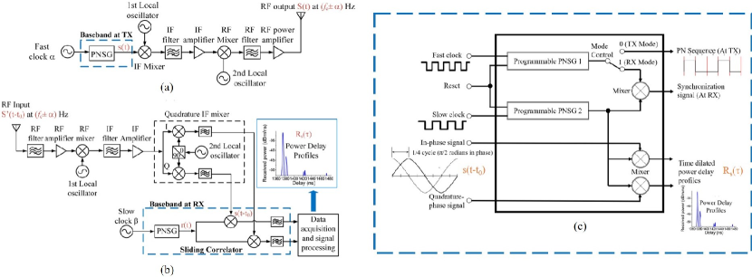
Fig. 1(a) and (b) are block representations of TX and RX setup in a sliding correlator based channel sounder [16]. In reference to Fig. 1(a), initially a PN sequence generator (PNSG) generates a PN sequence, , at a chip rate equal to the fast clock input, . The PNSG is implemented using maximal linear feedback shift registers with programmable feedback taps. At the subsequent mixer, modulates an intermediate frequency (IF) signal generated by the first local oscillator. The modulated signal at IF is upconverted to the RF carrier frequency, , resulting in the RF output signal at that is transmitted over the wireless channel. The wideband signal thus transmitted is subject to reflection, diffraction, scattering, and transmission through blockages in the channels before arriving at the receiver. The effects of the channel cause multiple replicas of the transmitted signal to arrive at the receiver over multiple paths at different delays. As illustrated in Fig. 1(b), the received multipath signals are down-converted and demodulated before sliding correlation is performed with a replica of the transmitted PN sequence operating at a slightly slower clock rate of , referred to as . The result of the sliding correlation process is a time dilated PDP that represents the time domain response of the channel, given by:
| (1) |
The dilation in the time scale of the received PDP corresponds to the sliding factor , obtained as in Eq. (2).
| (2) |
II-B Design of the on-board channel sounder IC
The dashed blue boxes in Fig. 1(a) and (b) represent the baseband components of the TX and RX which is combined by the channel sounder chip design on a monolithic IC design that is capable of operating at either end of the channel sounder system. As shown in Fig. 1(c), the ‘Mode Control’ pin on the IC is used to switch between TX mode for the pin set to ‘Low’ and RX mode for pin set to ‘High’.
The output of PNSG 1 directly generates PN sequence at chip rate of in TX mode. In RX mode, the output of PNSG 1, , is mixed with the output of PNSG 2, at chip rate , to generate the synchronization signal which is a zero delay absolute timing reference for the multipath components arriving at the receiver. The signal is also fed into two mixers in order to perform the sliding correlation function with the in-phase and quadrature components of the demodulated received signal. The output of the two mixers constitute the result of the sliding correlation function, .
III Design and Testing of the EVB components
III-A Channel Sounder IC Specifications based on Measurements
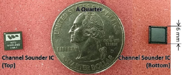
Fabricated in a 65 nm CMOS process, the channel sounder chip is a monolithic design of 1 mm 0.66 mm silicon, packaged in an industry standard QFN48 IC package of 6 mm 6 mm, as displayed in Fig. 2, and is the centerpiece of the EVB design [16, 19, 20].
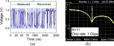
Initial tests with the chip directly wire bonded to a printed circuit board (PCB), and a 1.1 V supply voltage verified the sequence accuracy, chip rate, and bandwidth for different lengths of PN codes. Upon feeding with a 1 GHz clock signal as and programming a sequence length of 2047 (), the chip sequence was observed in time domain as the black trace in Fig. 3(a). Peak-transitions in the analog waveform higher than 0.5 V were recorded as ‘1’, else ‘0’ to obtain the blue trace and verify valid strings of same consecutive bits (runs) in the sequence. The spectrum measurement for the 1 Gbps PN sequence was as shown in Fig. 3(b) with the power profile showing a distinct energy peak of -18.4 dBm at 1 GHz, indicating 2 GHz null-to-null RF bandwidth. Specifications of the chip following the initial testing are tabulated in Table I [16].
| Item | Specification |
|---|---|
| Technology | 65 nm CMOS |
| Maximum Chip Rate | 1 Gbps |
| Multipath Delay Resolution | 1 ns |
| Null-to-Null RF Bandwidth | 2 GHz |
| PN Code Length |
(,
programmable) |
| Power Consumption | 6 mA at 1.1 V |
| IC Packaging | QFN48 66 mm2 |
| Synchronization | Supported |
III-B Layout of the EVB
The EVB design focuses on interfacing the wideband channel sounder IC to the 142 GHz channel sounding setup at NYU WIRELESS [15]. The board provides essential peripherals for the IC operation, which perform amplification and filtering of RF signals, inter-conversion between signal communication methods –differential and single-ended signaling, buffering and amplification of clock signals, and provide stable power supply at different voltages. Electronic components on the board are grouped into sub-units based on function and distributed over the board area according to the layout displayed in Fig. 4.
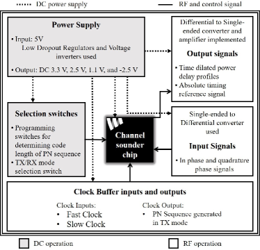
The board is laid out with sub-units operating at DC placed in a separate region from sub-units operating at frequencies up to 1 GHz. The separation of regions helps prevent interference on RF signal traces from the DC common-mode, and manage return paths within separated DC/RF ground planes. It helps preserve the integrity of signals near RX sensitivity (typically below -100 dBm) common at mm-Wave and THz frequencies.
III-C Design considerations for the EVB
Grounding: All signals flowing in a circuit seek the lowest impedance path to return to the signal power source to complete the circuit. As many signals are operating in a typical circuit, a single wire or trace of limited width and cross-section providing the return connection may have to carry hundreds of amperes current per of cross-section area [21]. Thus, a ground plane is a standard method of providing a broad cross-section for returning signal currents while minimizing the return path resistance. However, it is not a panacea for providing return paths to all signals as the behavior of returning currents varies by frequency. A DC signal returns over the shortest path on the ground plane, while RF signals seek out the path of minimum impedance [22]. For a two-layer PCB layout with signals routed on the top and ground on the bottom layer, RF signals above 1 MHz travel directly beneath the top layer signal trace. Furthermore, as DC signal return currents take the shortest path to ground, loops are formed on the ground plane, which may couple noise and interfere with RF signals.
RF signal traces routed on multi-layer PCBs require a continuous ground plane underneath without any slits and breakages along the entire return path. The presence of disruptions in the ground plane changes the path length for RF signals, as returning signals loop around the breakage[23]. For example, at a millimeter wavelength, the change in path length by a half-mm may put differential signals in-phase and change the path impedance to cause complete signal reflections.
Impedance of RF signal traces: Reflection of RF signals is avoided, and maximum power flow is maintained during the propagation of an RF signal over traces across the circuit board when the impedance is uniform throughout the signal path. Sub-miniature version-A (SMA) connectors with characteristic impedance of 50 are commonly used to transport RF signals over the wire in RF systems. Thus, RF signal traces with a continuous ground underneath, called micro-strip traces, are designed to have 50 characteristic impedance for RF-PCBs, as obtained from Eq. (3) [24].
| (3) |
The trace width () in Eq.(3) may be varied to achieve the 50 impedance. An extension to Eq. (3), shown in Eq. (4), is required to calculate the characteristic impedance for differential signal pairs as signals in a differential pair are referenced to each other and not to ground[24]. Finally, the trace length determines the input impedance offered by the trace and the connected load.
| (4) |
III-D Sub-units of the EVB and Test Results
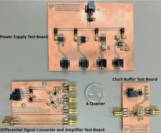
Before implementation on the final EVB, the sub-units were designed and tested on individual test PCBs. The test boards were fabricated in-house at NYU-MakerSpace on double-sided bare PCB with 18 m copper layers each side separated by 0.79 mm flame retardant-4 (FR-4) insulation material with a dielectric constant of 4.2. The fabricated test boards are displayed in Fig. 5. The sub-units are detailed as follows:
Single-ended signal converter and amplifier: To eliminate noise from the power supply, and thermal noise from external components that single-ended signals are subject to, the mixers and amplifiers in the chip baseband are designed for differential operation[25, 16]. However, the RF signals carried on coaxial cables interconnecting components of the 142 GHz channel sounder, setup at NYU WIRELESS are single-ended. Based on Fig. 1(b), to interface the chip input with the preceding IF mixer at the RX, each single-ended input signal from the IF mixers are split into two signals of equal magnitude but opposite polarity using a 50 700 MHz balun circuit. The implemented balun is a transformer with a 1:1 turns ratio between the primary and center-tapped secondary winding[26]. The primary is fed by the 500 MHz low pass filter output of the preceding IF mixers[15]. The secondary winding terminals of the balun circuit provide the differential input signals required by the chip.
In initial tests, a 500 MHz 100 mVp-p square wave was split into out-of-phase 44 mVp-p sinusoids, indicating a 0.5 dB insertion loss.
Differential signal converter and amplifier: A sliding correlation on two PN sequences results in a low-frequency time dilated PDP component with distortion components at a frequency above . This waveform is output by the chip in two components, each as a differential signal pair as in Fig. 1(b). The differential signal converter-and-amplifier merges the output signal pair into a single-ended signal, then low-pass filters and amplifies the single-ended signal, using the schematic shown in Fig. 6.
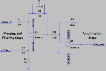
The merging and filtering stage outputs a single-ended signal with an amplitude equal to the difference between the two input signal amplitudes. The resistor (R3) and capacitor (C5) placed in parallel on the feedback line in Fig. 6 implement a first-order low-pass filter with a 3 dB bandwidth of 150 kHz to suppress the distortion component of the waveform. The amplification stage then amplifies the single-ended signal by gain equal to the ratio of resistances on the feedback line (R7) to the input line (R8) in Fig. 6, thus implementing a gain of 10 dB. The final board design implements a switch-selectable gain of 3, 10, or 20 dB.
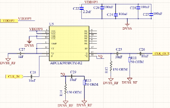
Clock Buffer: Clock signals are crucial to the implementation of a sliding correlator based channel sounder as they determine the rate of the PN sequence, bandwidth of the transmitted signal, and time dilation factor corresponding to . Direct distribution of the clock from a clock-source into different board components may degrade the waveform of the clock signal due to the added loading, noise from the on-board electronics, and cabling losses. For instance, a 10 pF additional stray capacitance can add a 200 mVp-p ringing distortion on a 500 mVp-p square wave[22]. Thus, the addition of a buffer between the clock source and clock dependent components can alleviate the waveform degradation and amplify the clock source prior supplying the components.
A 7.5 GHz state-toggling capacity clock buffer is implemented as a test board based on Fig. 7, for both the fast and slow clocks and in Fig. 1(c). Testing showed a consistent 600 mVp-p square wave output at the input clock frequency for input down to 60 mVp-p.
Power Supply: The components of the EVB require DC supply voltage at different levels; the clock buffer operates at 3.3 V, the differential signal converter and amplifier operates at 2.5 V, and the wideband channel sounder IC requires 1.1 V for biasing transistors and 2.5 V for driving input and output pins on the IC. The three positive voltages are generated with low dropout (LDO) voltage regulators [27], while the negative voltage is generated with a switched capacitor charge pump voltage inverter [28]. The current drawn by each of the test boards is measured with the power supply test board connected to a bench top regulated DC power supply at 5 V and the other boards connected to the voltage output ports of the power supply test board and is presented in Table II.
| Sub-Unit of EVB | Type | Supply voltage | Current draw (standby) | Current draw (active) |
| Power supply | Active | 5 V | 4 mA | 172 mA |
| Clock buffer | Active | 3.3 V | 1 mA | 44 mA |
| Differential signal converter and amplifier | Active | - 2.5 V/ 2.5 V | 1 mA | 5 mA |
| Single-ended signal converter | Passive | N/A | N/A | N/A |
| N/A: Not applicable | ||||
IV EVB Fabrication and initial measurements
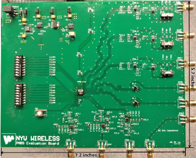
The final EVB is designed on a four-layer PCB with FR-4 dielectric insulation between layers. Micro-strip traces interconnecting components are routed on the top-layer with RF ground on the second layer plane. The third layer is used to distribute power supply lines and the bottom layer for grounding DC components in non-overlapping regions with the second layer. Further, the top-layer RF traces are shielded on either side by regions grounded with vias connected to the second layer RF ground. Such ground shielded traces minimize additional parasitic impedance from outward radiating fringing fields, prominent at mmWave and THz frequencies. Based on Eq. (3), the PCB has a top-layer copper of thickness (t) 1.4 mils, a separation (h) of 9.13 mils between each layer with FR-4 insulation of 4.2. Hence, an impedance of 50.01 is obtained for micro-strip traces with width (w) of 15.75 mils. Differential signal traces on the top-layer have a pair separation (d) of 25 mils for a differential impedance of 96.56 . The PCB features 50 SMA connectors to interface with external components. The final PCB layout of the channel sounder EVB is presented in Fig. 8.
Following component assembly, EVB operation yielded a peak current draw of 172 mA at 5 V input when generating a transmit PN sequence at of 1 GHz, with an energy peak of -30 dBm at 1 GHz in the measured spectrum power profile. The PN waveform showed consistent runs of ones and zeros, as described in [16], at 600 mVp-p for and input down to 70 mVp-p from 100 MHz to 1 GHz.
Conclusion
A wideband sliding correlator based channel sounder IC fabricated using 65 nm CMOS processes is featured in an EVB design for interfacing with the 142 GHz channel sounder system at NYU WIRELESS. The monolithic channel sounder IC design, using low-cost CMOS technology, achieves a remarkable 1 Gbps baseband operation; the EVB for the IC implements the baseband of an entire channel sounder setup with null-to-null RF bandwidth of over one GHz. This design reduces channel sounder system costs from hundreds of thousands to a few thousand dollars while reducing system complexity, compressing size to portable volumes, and delivering higher resolution channel measurements. Future research involves interfacing the EVB and channel sounder system and measuring the board performance in operation.
References
- [1] T. S. Rappaport, Y. Xing, G. R. MacCartney, A. F. Molisch, E. Mellios, and J. Zhang, “Overview of millimeter wave communications for fifth-generation (5G) wireless networks—with a focus on propagation models,” IEEE Transactions on Antennas and Propagation, vol. 65, no. 12, pp. 6213–6230, Dec 2017.
- [2] E. Dahlman, S. Parkvall, J. Peisa, and H. Tullberg, “5G evolution and beyond,” in 2019 IEEE 20th International Workshop on Signal Processing Advances in Wireless Communications (SPAWC), 2019, pp. 1–5.
- [3] M. Agiwal, A. Roy, and N. Saxena, “Next generation 5G wireless networks: A comprehensive survey,” IEEE Communications Surveys Tutorials, vol. 18, no. 3, pp. 1617–1655, Feb. 2016.
- [4] T. S. Rappaport, Y. Xing, O. Kanhere, S. Ju, A. Madanayake, S. Mandal, A. Alkhateeb, and G. C. Trichopoulos, “Wireless communications and applications above 100 GHz: Opportunities and challenges for 6G and beyond,” IEEE Access, vol. 7, pp. 78 729–78 757, 2019.
- [5] I. F. Akyildiz, J. M. Jornet, and C. Han, “Terahertz band: Next frontier for wireless communications,” Physical Communication, vol. 12, pp. 16–32, 2014.
- [6] Y. Xing, O. Kanhere, S. Ju, and T. S. Rappaport, “Indoor wireless channel properties at millimeter wave and sub-terahertz frequencies,” in 2019 IEEE Global Communications Conference (GLOBECOM), 2019, pp. 1–6.
- [7] O. Kanhere, S. Ju, Y. Xing, and T. S. Rappaport, “Map-assisted millimeter wave localization for accurate position location,” in 2019 IEEE Global Communications Conference (GLOBECOM), 2019, pp. 1–6.
- [8] Y. Xie, Z. Li, and M. Li, “Precise power delay profiling with commodity Wi-Fi,” IEEE Transactions on Mobile Computing, vol. 18, no. 6, pp. 1342–1355, 2018.
- [9] K. K.O., W. Choi, Q. Zhong, N. Sharma, Y. Zhang, R. Han, Z. Ahmad, D. Kim, S. Kshattry, I. R. Medvedev, D. J. Lary, H. Nam, P. Raskin, and I. Kim, “Opening terahertz for everyday applications,” IEEE Communications Magazine, vol. 57, no. 8, pp. 70–76, 2019.
- [10] M. J. W. Rodwell, “100-340GHz spatially multiplexed communications: IC, transceiver, and link design,” in 2019 IEEE 20th International Workshop on Signal Processing Advances in Wireless Communications (SPAWC), 2019, pp. 1–5.
- [11] J. Lee, J. Liang, J. Park, and M. Kim, “Directional path loss characteristics of large indoor environments with 28 GHz measurements,” in 2015 IEEE 26th Annual International Symposium on Personal, Indoor, and Mobile Radio Communications (PIMRC), Aug 2015, pp. 2204–2208.
- [12] G. R. MacCartney and T. S. Rappaport, “A flexible millimeter-wave channel sounder with absolute timing,” IEEE Journal on Selected Areas in Communications, vol. 35, no. 6, pp. 1402–1418, June 2017.
- [13] G. R. MacCartney, H. Yan, S. Sun, and T. S. Rappaport, “A flexible wideband millimeter-wave channel sounder with local area and NLOS to LOS transition measurements,” in 2017 IEEE International Conference on Communications (ICC), May 2017, pp. 1–7.
- [14] R. Miao, L. Tian, Y. Zheng, P. Tang, F. Huang, and J. Zhang, “Indoor office channel measurements and analysis of propagation characteristics at 14 GHz,” in 2015 IEEE 26th Annual International Symposium on Personal, Indoor, and Mobile Radio Communications (PIMRC), Aug 2015, pp. 2199–2203.
- [15] Y. Xing and T. S. Rappaport, “Propagation measurement system and approach at 140 GHz-moving to 6G and above 100 GHz,” in 2018 IEEE Global Communications Conference (GLOBECOM), Dec 2018, pp. 1–6.
- [16] T. Wu, T. S. Rappaport, M. E. Knox, and D. Shahrjerdi, “A wideband sliding correlator-based channel sounder with synchronization in 65 nm CMOS,” in 2019 IEEE International Symposium on Circuits and Systems (ISCAS), May 2019, pp. 1–5.
- [17] D. Cox, “Delay Doppler characteristics of multipath propagation at 910 MHz in a suburban mobile radio environment,” IEEE Transactions on Antennas and Propagation, vol. 20, no. 5, pp. 625–635, 1972.
- [18] R. J. Pirkl and G. D. Durgin, “Optimal sliding correlator channel sounder design,” IEEE Transactions on Wireless Communications, vol. 7, no. 9, pp. 3488–3497, 2008.
- [19] I. Post, M. Akbar, G. Curello, S. Gannavaram, W. Hafez, U. Jalan, K. Komeyli, J. Lin, N. Lindert, J. Park, J. Rizk, G. Sacks, C. Tsai, D. Yeh, P. Bai, and C. . Jan, “A 65nm CMOS SOC technology featuring strained silicon transistors for RF applications,” in 2006 International Electron Devices Meeting, 2006, pp. 1–3.
- [20] Yeong-Lin Lai and Cheng-Yu Ho, “Electrical modeling of quad flat no-lead packages for high-frequency IC applications,” in 2004 IEEE Region 10 Conference TENCON 2004., vol. D, 2004, pp. 344–347 Vol. 4.
- [21] Yi Wang, S. W. H. de Haan, and J. A. Ferreira, “Thermal design guideline of PCB traces under DC and AC current,” in 2009 IEEE Energy Conversion Congress and Exposition, 2009, pp. 1240–1246.
- [22] H. Zumbahlen, “Staying well grounded,” Analog Dialogue, vol. 46, no. 2, p. 17, 2012.
- [23] S. Pithadia and S. More, “Grounding in mixed-signal systems demystified, Part 1,” Analog Applications, 2013.
- [24] M. Graham and H. Johnson, “High-speed digital design: a handbook of black magic,” University of California at Berkeley, 1993.
- [25] B. Razavi, Design of analog CMOS integrated circuits. Tata McGraw-Hill Education, 2002.
- [26] D. Jorgesen and C. Marki, Balun basics primer, Marki Microwave, 2014.
- [27] M. S. W. Fwu, A. Paxton and J.G.Torres, LDO Basics, Texas Instruments, 2018, rev. A.
- [28] A. Bindra, Generating Negative Output from Positive Input Voltage, DigiKey, 10 2012, electronic Products.