Measurements of the magnetic properties of conduction electrons
Abstract
We consider various methods and techniques for measuring electron magnetization and susceptibility, which are used in experimental condensed matter physics. The list of considered methods for macroscopic measurements includes magnetomechanic, electromagnetic, modulation-type, and also thermodynamic methods based on the chemical potential variation measurements. We also consider local methods of magnetic measurements based on the spin Hall effects, NV-centers. Several scanning probe magnetometers-microscopes are considered, such as magnetic resonance force microscope, SQUID-microscope, and Hall microscope. The review focuses on the spin magnetization measurements of electrons in non-magnetic materials and artificial systems, particularly, in low-dimensional electron systems in semiconductors and in nanosystems, which came to the forefront in recent years.
I Introduction
Due to the additivity of thermodynamic quantities, measurements of any of them become challenging with reducing the size of the studied sample. Experimentalists face with this problem even when dealing with small three-dimensional objects such as, for example, “whiskers” of Zn, Bi, Sn, whose typical sizes are m3.
Indeed, the magnetic susceptibility of nonmagnetic metals is typically , therefore, the magnetization of such a sample in a field of Oe is CGS, that is several orders of magnitude less than the sensitivity threshold of traditional laboratory magnetometers - torsion- griessen_1973 ; vandrkooy_1969 , Faraday- (or “magnetic balance”), vibration-type (so-called, Foner-magnetometer) foner_1959 , and others.
For such small samples, the change in magnetic susceptibility by 1% in a field of Oe will cause a change in the magnetic flux through the sample crossection m2 of about CGS, which is approximately flux quantum and also lies beyond the sensitivity threshold of SQUID magnetometers.
This seemingly purely technical problem for a long time remained an obstacle to studying magnetic properties of two-dimensional (2D) electron systems in which the effective thickness of the electron layer is of the order of the Fermi wavelength )Åand where the typical number of electrons in the sample is total .
The characteristic energy associated with the sought for changes in magnetic properties are not so small, meV per electron. This obviously means that the difficulty of measuring the magnetic properties of two-dimensional and ultrathin samples are associated not with a smallness of the effects, but with the inadequacy of traditional methods for measuring the properties of samples of small thicknesses.
Clearly, to overcome the problem, different measurement methods are needed in which the signal magnitude does not decrease proportionally to the sample volume. This review addresses a number of such, in fact, classical methods that were successfully used in practice.
In the field of condensed matter magnetometry there is a review by Usher and Elliot usher09 , which considers classical methods for measuring orbital electron magnetization, and their application for studying the quantum Hall effect and related phenomena. There are also a number of monographs (eg, chechernikov_book ), where techniques are considered for measurements with ferromagnetic materials. In this review, unlike usher09 ; chechernikov_book , the focus is on the methods for measuring spin rather than orbital magnetization of electrons in non-magnetic materials, the former is usually much less than the orbital one.
For completeness and reader convenience this review also briefly mentioned not only the spin magnetism, but also the orbital magnetism of electronic systems, including those that have already been described in usher09 . However, we supplement this description with some results omitted in usher09 .
Further, the review describes more modern methods developed in the last 20 years, in connection with with the task of studying the spin properties of strongly correlated electrons in low-dimensional systems. Recently, thermodynamic methods turned out to be among the most fruitful; they are based on measurement of chemical potential derivatives for the two-dimensional systems. The consideration is accompanied by a description of several key physical results obtained by these methods.
Finally, the review considers local methods of measurements, including various types of scanning magnetic microscopes, booming recently in connection with the numerous tasks of spintronics, manipulating with single spins, biophysics, and virology.
II Traditional methods of electron magnetization measurements
II.1 Electromechanic methods
These methods can be divided into two classes:
(a) based on the measurements of the force acting on a
sample in an inhomogeneous magnetic field
(Faraday magnetometer), or torque - in case of an anisotropic sample in a uniform magnetic field (torsion magnetometer) and
(b) based on electromagnetic
induction measurements (Foner magnetometer).
II.1.1 Torsion magnetometer
This type of magnetometer is based on “torsion balance” introduced in the everyday use of experimental physics at the end of the 18th century by C.-A. de Coulomb to measure electrical forces, and by H. Cavendish - for measuring gravitational forces. In the contemporary experimental physics, laboratory magnetometers are ubiquitous for measuring in a uniform field B the torque acting on an anisotropic sample. In the torsion magnetometers, this torque is compensated by forces from an elastic element deformation.
II.1.2 Torsion magnetometers with electric detection
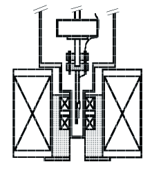
To measure the deformation of an elastic element, capacitive, inductive, or optical sensors are used. Capacitive deformation sensors griessen_1973 starting from the 1960s to the present were successfully used for measurements of the oscillatory magnetization (de Haas-van Alphen effect, dHvA). In regard to the problem of measuring magnetic properties of low-dimension systems, the torsion balance scales were adapted by Eisenstein et al. to measure the dHvA effect for electrons in a 2D system eisenstein_APL_1985 ; eisenstein_PRL_1985 ; design of these scales is shown schematically in Fig. 1. The sample - GaAs-AlGaAs heterostructure - with 2D electron gas is attached to a thin elastic thread (Pt-W, with a diameter of 37m and 2 cm long), stretched perpendicular to the magnetic field direction. The orbital magnetic moment of electrons in 2D systems is the partial derivative of the free energy with respect to magnetic field:
For isotropic samples (ignoring geometric demagnetizing factor), the field-induced magnetic moment is parallel to and, therefore, the torque does not arise. For a 2D electron system the induced orbital moment is always directed normal to the 2D plane, due to cyclotron motion in the 2D plane. This magnetic moment causes a mechanical torque acting on the sample
where the second term arises in inhomogeneous magnetic field and - is the vector-arm of the applied torque relative to the totation axis.
The torque L leads to twisting of the elastic thread until the forces of its elastic deformation do not compensate the applied torque. The angle of the thread rotation is detected, for example, by a capacitance changes.
For a small twisting angle , the restoring mechanical moment of the twisted elastic thread is , where is the angle between the field direction and the normal to the plane. While the deviations from the equilibrium are small, , torsion scales operate linearly with .
The authors eisenstein_APL_1985 ; eisenstein_PRL_1985 estimated the sensitivity limit for thread twisting as rad, and the magnetometer in total - as J/T (or CGS) in field of 5 Tesla, that is equivalent to Bohr magnetons. For detecting the de Haas van Alphen effect (dHvA) with such a relatively low magnetometer sensitivity the authors used a GaAs/AlGaAs heterostructure containing a large number of parallel connected 2D electron sheets with a total area of 2 cm2 eisenstein_APL_1985 , and even 12.5 cm2 eisenstein_PRL_1985 . Due to the nonlinearity of capacitance changes with angle (disc misalignment), the the amplitude m was measured in Ref. eisenstein_APL_1985 ; eisenstein_PRL_1985 with 25% uncertainty.
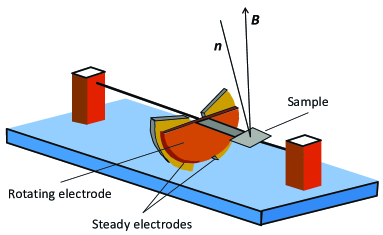
A different design of the torsion magnetometer with a capacitor more sensitive to the angle of sample rotation was developed by Templeton templeton_JAP_1988 and was later applied with some improvements in a number of works jones_SSC_1995 ; matthews_RSI_2004 ; matthews_PRB_2004 . In this design, twisting the thread with the sample and the capacitor plate cause changes in the effective capacitor gap rather than the plates area. As a result, relative capacitance changes amounts , rather than , as in the design Fig. 1, giving a gain in the threshold sensitivity by an order of magnitude.
Due to the small gap mm between the capacitor plates, the magnetometer threshold resolution, in terms of the rotation angle , in this design could be a factor of better than in the magnetometer Fig. 1, though in practice it appeared to be improved only by 10 times being limited by vibrations. Another advantage of this design is the possibility of applying electrostatic (ponderomotor) force, by applying a DC voltage between the capacitor plates. Such a feature is useful for damping the rotation system dynamics, for calibrating absolute value of the elastic torque (in situ, in the course of experiment), as well as for introducing a feedback and, thereby linearizing the amplitude response characteristics of the magnetometer.
Threshold resolution was J in terms of the detectable torque, and rad in units of the detectable rotation angle, or - relative change in capacitance. This resolution enabled detecting dHvA oscillations for a single heterojunction of 8 mm2 area, with a total number of electrons .
Since all torsion magnetometers are based on a freely suspended electromechanical system, the main source of noise are vibrations. Wiegers et al. wiegers_RSI_1998 ; wiegers_PRL_1997 described the design more resistant to vibrations because it contains a cylindrically symmetric rotor capacitor, and the sample is located in the center mass of the rotary unit.
These design features have reduced a parasitic link coupling with external vibrations. The resonant frequency of the suspended system is 1.5Hz, and the sensitivity threshold of this magnetometer can be estimated from the reported measurements of the oscillatory signal as per electron, although slow variations of the background were a factor of 10 larger wiegers_RSI_1998 ; wiegers_PRL_1997 . The authors estimated the threshold magnetometer sensitivity as J/Tesla, which is equivalent to Bohr magneton in field of 1 T.
II.1.3 Torsion magnetometers with optical detection
In torsion magnetometers with capacitive sensors, the detecting bridge circuit is fed with a low frequency AC voltage that can induce unwanted emf at the sample contacts.
In Refs. schaapman_APL_2002 ; bominaar_NJP_2006 , an optical technique was used for sample deviations detecting. For this purpose, a laser beam was introduced into a cryostat via a multimode fiber, reflected from the sample and then reached photodetector. The magnetometer was successfully used schaapman_PRB_2003 for measuring electron magnetization of quasi-two-dimensional organic small crystals (weighing 0.13 mg), as well as for magnetization measurements with GaAs double quantum wells bominaar_NJP_2006 , and single layer GaAs/AlGaAs heterostructure schaapman_APL_2002 . Threshold sensitivity J/Tesla in field of 15 T corresponds to magnetization changes per electron. Optical detection turned out to be workable even for measurements in the field of Bitter magnet, which creates a fairly large electrical noise. In this case, the threshold sensitivity was albeit lower by an order of magnitude, but still was enough for studying quantum oscillations of magnetization single- schaapman_PRB_2003 and double-layer heterojunctions GaAs/AlGaAs bominaar_NJP_2006 .
II.1.4 Microconsole-type magnetometers
The operation principle of these magnetometers is similar to the torsion balance. Just like in the latter, the torque acting on a sample from the magnetic field, is balanced by mechanical torque of elastic forces. The difference is that the elastic element undergoes bending deformation rather than torsion.
In Ref. whiskermagnetometer-PTE_78 , a “flexural” magnetometer is described, in which the sample is not integrated in a single process with the console, but itself plays a role of the bending element. Thus, the torque acting on the sample causes bending the sample itself, and not the auxiliary elastic element. The sample - a flat threadlike crystal (whisker) m thick and m long is placed in magnetic field tilted by relative its plane.
One end of the sample is firmly fixed. Magnetic field induces the torque . According to the elasticity theory, the resulting bending of the sample, characterized by a certain average angle is equal to:
| (1) |
where -the elastic modulus, is the thickness, -sample width, and - is a factor of the order of unity.
As can be seen from this equation, the bending angle is inversely proportional to , while the torque itself is proportional to the sample volume, i.e. thickness . Thus, with a decrease in the sample thickness, the bending angle does not decreases, but increases! The measured bending angle is is a measure of the mechanical torque , and therefore of the magnetic moment M.
Using this magnetometer, quantum magnetization oscillations were measured for a threadlike Bi crystal with sizes m3 whisker-jdPhys_78 . The bending angle for such sample in this case was rad, and magnetic moment changes CGS.
In order to linearize the characteristics in the device, a feedback is introduced by applying voltage between the sample and a closely located metal plane. The torque of electrostatic forces acting on the sample compensates for the measured torque . For a large amplification factor in the feedback circuit, the angle practically does not vary, and the value is the measure of the sought for magnetization signal . Due to the feedback, the dynamic range the measured moment was 4 orders of magnitude, i.e. 80 dB whisker-jdPhys_78 . The noise level of the magnetometer was dynecm in the 1 Hz bandwidth.
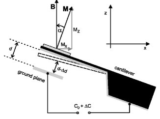
With the development of microtechnologies at the end of the past century, micromechanical cantilever (or console) magnetometers (MCM) have been designed, based on both silicon - naughton_PhysicaB_1998 ; wilde_PRB_2005 , and GaAs technology harris_APL_1999 ; schwarz_APL_2000 . Figure 2) shows a flat sample with 2D electron gas mounted at the end of the elastic microconsole. External magnetic field B is applied at an angle to the sample plane.
Since orbital electron magnetization vector is perpendicular to the 2D electron gas plane, console with the sample experiences a mechanic torque . Thus, the sought for magnetic moment, in the first approximation, is proportional to the angle of deformation of the elastic beam.
The operation principle of the micro-console magnetometer is illustrated in Fig. 2 from wilde_PRB_2005 : the sample, glued at the end of the console, is a substrate of 1mm2 area with Si/SiGe heterojunction containing 2D electron system; for reducing weight, the SiGe substrate is thinned to m. The console with the sample is directed at an angle relative to the magnetic field B vector; changes of the magnetic moment, proportional to the torque , are directly related with the console bending angle: . Typical thickness of the bending element - beam - is m schwarz_APL_2000 .
The micro-console magnetometers provide a high sensitivity. In particular, in Ref. schwarz_APL_2000 the threshold sensitivity was J/T, (Nm) or , i.e. per electron. In experiment wilde_PRB_2005 , using this magnetometer, quantum magnetization oscillations for 2D electron system in SiGe were reliably detected starting from field of 1 T.
Due to this, in Ref. wilde_PRB_2005 the authors were able to study Landau levels broadening, valley and spin splitting and their renormalization in magnetic field. In experiments schwarz_PRB_2002 ; wilde_PRB_2006 with GaAs/AlGaAs heterojunction, the authors measured the density of states profile at the Landau levels minima of the density of states, amplitude of oscillations in absolute units, as well as enhancement of the spin splitting caused by exchange interaction between the Landau levels. In the experiment with ZnSe/Zn1-x-yCdxMnySe quantum wells knobel_PRB_2002 the evolution of extended states at the Landau levels with levels broadening was studied.
In most of the magnetometers naughton_PhysicaB_1998 ; wilde_PRB_2005 ; schwarz_APL_2000 ; schwarz_PRB_2002 ; wilde_PRB_2005 , bending of the micro-console was detected via changes in the capacitance of the capacitor, with a gap between the plates from m wilde_PRB_2005 , 50 m schwarz_PRB_2002 to m harris_PRL_2001 .
Beside the capacitive method of measuring beam deformation, in a number of MCM designs harris_PRL_2001 ; ruhe_PRB_2006 an optical technique was used, similar to that considered above for the torsion magnetometers. Exclusion of electrical measurements of capacitance at AC current allows, in principle, to get rid of cross interference on the sample and, due to this, enables simultaneously with magnetization measurement to measure DC transport- properties.
For measurements of the magnetic moment for a ferromagnet semiconductor Ga1-xMnxAs in harris_APL_1999 ] was used another way – to measure the shift of the vibration eigen frequencies of the console. The elastic beam in the magnetometer harris_APL_1999 had a transverse dimensions of m2, m length, resonant frequency 1600 Hz and the Q-factor 11500. A sample with dimension 2 was installed at the end of the beam. With these parameters, a threshold sensitivity was shown to be in field of 0.1 T and in the 1Hz bandwidth harris_APL_1999 .
The obvious advantage of MCM is their miniature design, as well as a short response time, since the resonant frequency of the beam is approximately inversely proportional to its length. In practical constructions, the resonant frequency is kHz naughton_PhysicaB_1998 , allowing use of such magnetometers for measurements in pulsed fields. Of course, for applications even in “long” pulse magnetic fields, of the order of tens of ms, the mass of the sample should be small, of the order of mg; generally, for static measurements, the mass is limited by mg, due to unbalanced gravity. In some of these devices harris_APL_1999 ; schwarz_APL_2000 ; ruhe_PRB_2006 , the micro-console is integrated into a single unit with the sample – GaAs-based heterojunction substrate with two-dimensional electron gas.
It is worthy of noting a related to MCM local magnetometry technique – scanning magnetic force microscope (MFM), to be briefly considered further in section V.3.1.
II.1.5 Vibrating-type magnetometer
In vibrating magnetometers (VM), the measured signal is the EMF induced by mechanical vibration of the sample relative to a pick-up coil, placed in a constant magnetic field. Vibrating magnetometer was invented by S. Foner foner_1956 and described by him in detail in Ref. foner_1959 . In the original design foner_1956 ; foner_1959 the sample vibration was driven by the laud speaker cone in the direction perpendicular to magnetic field. Threshold sensitivity in terms of the susceptibility the author estimated as in the frequency bandwidth Hz foner_1959 and in terms of magnetization – as CGS in field of 1 Tesla foner_1996 .
Review foner_1996 considers various options of the pick-up systems for detecting the induced AC magnetic field, including SQUID magnetometers. There are also considered various examples of VM in cryostats with 3He pumping, dilution refrigerators, and in hydrostatic pressure cells guertin_PRL_1976 ; guertin_LT_1978 . An “inverse” design of a VM is described in reeves_1972 , in which the sample is likewise placed in the bore between two coils. However, the coils are used not for receiving the induced voltage, but generate an alternating magnetic field. As a result, the sample experiences a force causing its vibrations which are detected with piezo-sensors.
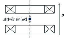
When superconducting coils are used (in contrast to the electromagnet with a gap between the magnet poles as was in the first works foner_1956 ; foner_1959 ; foner_1996 ) in the modern vibration magnetometers springfort_1971 ; johansson_1976 ; hoon_1988 ; ausserlechner_1996 ; nizhankovskii_2007 , the sample moves parallel to the magnetic field of the solenoid, rather than perpendicular. Figure 3 shows a schematic design of the pick-up coils system for this geometry called “vibrating sample magnetometer” (VSM).
Let a sample with a magnetic moment be placed at an average distance from the plane of the pick-up coil with a radius . The sample sizes are presumed to be much less than and . The reciprocal motion of the sample along magnetic field induces an emf in the pick-up coil springfort_1971 ; braggt_1976 ; johansson_1976 ; hoon_1988 ; ausserlechner_1996 ; nizhankovskii_2007 :
where - is the angle, surrounding the coil perimeter from the point of sample location, and the transverse dimensions of the coils are assumed to be much less and . For a pair of identical opposite-connected coils, spaced apart along the solenoid axis, the sample deviation from the center by the distance induces an emf:
| (2) | |||||
| (3) |
A detailed analysis of the emf induced in the pick-up coils of various geometries and for their various location is given in Ref. ausserlechner_1996 . The amplitude of the induced voltage has a maximum at , however for achieving the most “flat” characteristics (weakly sensitive to radial deviation of the sample middle point from the ideal position) usually is chosen springfort_1971 .
For driving the sample vibration, several techniques are now used: electric motors with lowering gears johansson_1976 , bimorph piezo-elements mangum_1970 , crankshaft mechanisms hoon_1988 and stepper motors nizhankovskii_2007 . The threshold sensitivity of VSM typically ranges from CGS johansson_1976 ; nizhankovskii_2007 to CGS mangum_1970 .
With an increase in the amplitude of oscillations, even harmonics appear in the picked-up EMF in receiving coils. In Ref. ausserlechner_1996 , the amplitude of the second harmonic was used for absolute calibration of VSM; this method is conceptually similar to the one discussed below – finding the magnetization amplitudes for a nonlinear oscillator pudalov74 .
Vibrating sample magnetometers have proven to be reliable and convenient tools and until now are produced by a number of manufacturers of scientific equipment cryogenic .
II.1.6 Summary
The described above electromechanical and electromagnetic magnetometers provide possibility of taking measurements of the thermodynamic magnetization in absolute units. For the majority of them (except some console-type), naughton_PhysicaB_1998 ) magnetization measurements are performed under slow magnetic field sweeping or at a constant field. For lowering unwanted vibrations effect, all these instruments have a low resonant frequency of their elastic mechanical system, Hz, and therefore field modulation is not used. As a result, the magnetometers are rather slow and beside the oscillatory magnetization detect an unwanted slow monotonic background signal, related with drifting environment parameters, drifting the construction and magnetism of its elements, etc. Despite all these shortcomings, due to the simplicity of design, VSM are widely used and are commercially available for laboratory applications.
Obviously, to reduce the effect of drift, it is necessary to increase the modulation frequency of the signal. The only parameter allowing fast modulation is the concentration of electrons that can be changed in 2D structures by varying the gate voltage. This modulation method is described below in section II.2.2.
II.2 Electromagnetic type magnetometers
II.2.1 SQUID-magnetometer
The first measurements of the magnetization quantum oscillations for 2D electron sheet were done in Refs. stormer-dHvA_JVST_1983 ; havasoja_SSci_1984 , namely using the SQUID-magnetometers. By now, a large number of laboratory instruments are described in the literature, besides, the SQUID-magnetometers are commercially available; for this reason we don’t consider, but only briefly mention them here. In Refs. stormer-dHvA_JVST_1983 ; havasoja_SSci_1984 the authors used a commerical SQUID-magnetometer, whose threshold sensitivity was insufficient for detecting quantum oscillations of a single two-dimensional layer of electrons with density cm-2. For this reason, the authors used a set of 23 parallel GaAs-AlGaAs heterostructures, each with 173 two-dimensional layers (quantum wells), in total of parallel connected 2D layers of the 240 cm2 area. As a result, the authors for the first time observed quantum oscillations (de Haas-van Alphen effect) for 2D electron system.
In a more advanced design meinel_APL_1997 the threshold sensitivity was improved more than by three orders of magnitude; as a result, the authors registered quantum oscillatory magnetization for electrons in a GaAs-AlGaAs heterostructure with 7 mm2 area. Subsequently, they were able to study electron magnetization in the fractional quantum Hall effect regime meinel_PRL_1999 .
In the SQUID magnetometer meinel_APL_1997 , a thin film SQUID sensor was used with integrated multi-turn superconducting coil. The first-order gradiometer was connected to the input superconducting coil, creating a flux transformer. Sample with 2D electron system was positioned in one of the reception pick-up loops of the gradiometer. SQUID itself was located in a remote cryostat and was shielded from the stray magnetic field. To reduce noise, measurements were carried out by modulating the gate voltage of the 2D heterostructure, at a frequency of 1.2 kHz, at which the SQUID noise level was the smallest. In the absence of a field, the noise level of the magnetometer was , (for electrons in the sample), however, the noise increased with field, by approximately a factor of 10 already in the field of 6 Tesla.
II.2.2 Modulation technique of magnetic susceptibility measurements
The total orbital magnetization for a typical sample of a cm2 area with the number of electrons in the field Tesla amounts to only CGS. In order to measure such a small quantity it is necessary to use the above rather complex electromechanical constructions, poorly compatible with magnetic field modulation. For solving this technical problem, Fang and Styles fang-stiles_PRB_1983 modulated the electron concentration, rather than external magnetic field. Implementation of the much higher frequency reduces the most difficult problem of a low frequency noise. In the experiment fang-stiles_PRB_1983 the gate voltage of the gated structure was modulated at a frequency of 100 kHz, and for receiving the induced signal, a thin film coil was fabricated on the surface of the insulating Al2O3 layer, deposited atop the Al gate.
In order the picked-up alternating magnetic field would not be shielded by the conducting polysilicon gate, the latter was lithographically split into 20 strips, each m wide. Under harmonic modulation of the gate voltage , and, accordingly, modulation of electron concentration in the two-dimensional layer , the voltage induced in the receiving coil is proportional to the oscillatory component :
| (4) |
where is the magnetic flux across the pick-up coil, – total area of the two-dimensional channel, – capacitance of the gated MOS structure, - electron effective mass, and is the Landau level number.
The latter equation has no fitting parameters; sample dimensions, area and capacitance are easily determined. Despite this apparent simplicity, measurement of the absolute amplitude of oscillations with this technique is impeded by the recharging time of the MOS structure which for correct amplitude measurements should be much smaller than the modulation period. In practice, this requirement can hardly be fulfilled, especially when approaching the quantum Hall effect where the conductivity of the 2D system drops exponentially (and therefore, recharging time increases) in a two-dimensional structure pudalov_SSC_1984 ).
II.2.3 Oscillatory magnetization measurements in a system with nonlinear magnetization
In Ref. pudalov74 , a method was proposed and implemented for measuring the amplitude of the electron magnetization oscillations from quantum oscillations of any other quantity (specifically, for example, magnetostriction), under nonlinear conditions of magnetic interaction. The parameter measured in this method is the shape or the spectrum of quantum oscillations; it does not decrease proportionally to the sample volume, this feature in principle does make it applicable to systems with a small number of electrons. The method is based on the fact that despite the smallness of the magnetization oscillations , i.e. the amplitude of the dHvA effect, the oscillation period for large Fermi surfaces is also small and therefore the differential magnetic susceptibility becomes comparable with . As the result, magnetic induction in the sample differs significantly from the external field, . This difference causes the so called “magnetic interaction” or “Shoenberg effect” shoe_68 (here, is the demagnetizing factor). Magnetization is determined self-consistently by solving the exact nonlinear equation pippard
| (5) |
where - is the circular oscillation frequency for the given extremal FS cross-section , and is the oscillatory harmonic number in the Lifshitz-Kosevich formula LK_JETP_1955 ; isihara-JPC_1986 . In Ref. pudalov74 this equation was solved by successive approximations and the amplitude of magnetization quantum oscillations (orbital electron magnetization) has been determined by comparing spectrum of the measured oscillations with solution of equation (5).
The described above pioneer experiments stormer-dHvA_JVST_1983 ; fang-stiles_PRB_1983 ; pudalov74 have demonstrated a possibility of measuring orbital electron magnetization in non-magnetic metals and semiconductors, however, in view of the complexity of the methods used, and their inherent shortcomings, in the future they were little used.
III Electron spin susceptibility from charge transport measurements
III.1 Spin susceptibility from monotonic magnetotransport in the in-plane field
In order to get information on the spin susceptibility
of electron systems from monotonic magnetotransport,
measurements are performed (a) in strong
fields (), or (b) in weak fields
().
III.1.1 High field measurements
The first method is based on the empirical fact that for the ideal (zero thickness) 2D system, the in-plane magnetic field couples only with the spin degree of freedom. When magnetic field reaches the complete spin polarization value, the magnetoresistance of a 2D system exhibits a feature (in Si-MOS and Si/SiGe the magnetoresistance saturates) gold-dolgopolov_JETPL_2000 ; shashkin_PRL_2001 ; pudalov_PRL_2002 ; tutuc_PRL_2002 ; gold_PRB_2003 ; das_PRB_2005 ; gao_PRB_2006 ; lu_PRB_2008 ; from the position of this feature in a number of works, the renormalized spin susceptibility value was determined. Here and are the renormalized g-factor and effective mass of electrons, respectively.
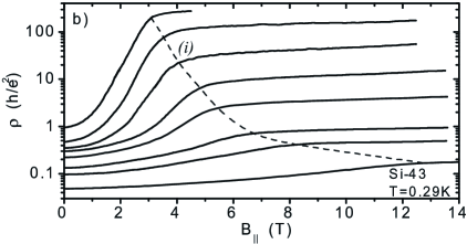
The advantage of this method is the simplicity of measurements and apparent simplicity of data interpretation. The disadvantages are connected, firstly, with perturbative action of strong fields which “cut off” temperature dependence of altshuler_JETPL_1982 , secondly, with the field influence on the value due to the nonlinear character of magnetization zhang-das_PRL_2006 , and thirdly, with disorder effect on the measured magnetoresistance saturation field pudalov_PRL_2002 ; vitkalov_PRB_2002 ; sara_JPSJ_2003 . Nevertheless, several works tutuc_PRL_2002 reported the consistency of the values, obtained from the spin polarization field and by other techniques, considered below.
III.1.2 Measurements in low and zero field
Quantum corrections to magnetoconductivity in weak field originate from the dependence of the effective number of triplet channels of electron-electron interaction on Zeeman splitting. From the magnetoconductivity measured in weak field , or from temperature dependence of the conductivity in zero field one can extract the quantum interaction corrections altshuler_JETPL_1982 . According to theory ZNA_PRB_2001 , their magnitude depends on via the Fermi-liquid coupling constant in the channel:
| (6) |
In equation (6), the first and second terms describe e-e interaction correction in the singlet and triplet channels, respectively, is the number of triplet channels ( for (001)-Si in weak field and for not too low temperatures vitkalov_PRB_2003 ; klimov_PRB_2008 ). In the ballistic interaction regime (of “high” temperatures)
| (7) | |||||
| (8) |
For the low-temperature diffusive regime of interactions, the interaction correction depends logarithmically on temperature altshuler_JETPL_1982 ; ZNA_PRB_2001 .
Extracting quantum correction from transport in zero field is relatively easy performed in the ballistic regime, from the measured quasi-linear -dependence ; as a result of such approach, a number of works shashkin_PRB_2002 ; coleridge_PRB_2002 ; kvon_PRB_2002 ; proskuryakov_PRL_2002 ; safonov_JPSJ_2003 ; noh_PRB_2003 ; noh_JPSJ_2003 ; kvon_PRB_2003 ; pudalov_PRL_2003 ; savchenko_Phys E_2004 reported measurements of the interaction-renormalized - factor as a function of the carrier density.
For nonzero magnetic field, and within the same ballistic regime, interaction quantum correction to magnetoconductivity
| (9) |
depends quadratically on field and inversely on temperature ZNA_PRB_2001 ; vitkalov_PRB_2003 , that in principle enables to determine .
However, the -factor values determined in such way from magnetotransport, as a rule, lead to -values not fully consistent with the ones, determined from dependence pudalov_PRL_2003 ; vitkalov_PRB_2002 ; klimov_PRB_2008 . One of the reason is the dependence of theoretical expression for quantum correction on the character of disorder potential ZNA_PRB_2001 ; gornyi_PRB_2004 ; gornyi_PRL_2003 , which for the real 2D systems is poorly known clarke_NatPhys_2007 . Another cause of the discrepancies is related to the difficult disentangling of the interaction quantum corrections from classical and semiclassical magnetoresistance effects proskuryakov_PRL_2003 ; morgun_PRB_2016 .
In the “low-temperature” diffusive interaction regime , in weak fields , according to theory ZNA_PRB_2001 , quantum correction to the nagnetoconductivity is proportional to :
Their disentangling from the semiclassical magnetoresistance represents rather hard task kuntsevich_PRB_2013 ; morgun_PRB_2016 (for more detailed discussing this issue - see kuntsevich_PRB_2013 ; morgun_PRB_2016 ; pudalov_JSNM_2017 ).
The disadvantages of all considered in this section transport-type methods of -factor measurements is their indirect character; clearly, their results depend on the theoretical models, on simplifying assumptions, etc. Additional complicating factor is the dependence of the spin polarization field on disorder pudalov_PRL_2002 ; vitkalov_PRB_2002 ; sara_JPSJ_2003 . Finally, all the above methods enable to determine only the renormalized -factor , whereas the effective mass , needed to determine , must be found from other measurements, for example from temperature dependence of the quantum oscillations amplitude; the oscillatory methods and effects are discussed below.
III.2 Spin susceptibility from quantum oscillations in tilted magnetic field
The simplest and most widely used method of the spin susceptibility measurements for two-dimensional electron systems fang_PRB_1968 ; okamoto_PRL_1999 ; zhu_PRL_2003 ; shayegan_PRB_2008 was suggested and first implemented by F. Fang and P.J. Styles fang_PRB_1968 . It consists of magnetoresistance oscillation measurements (SdH effect) in magnetic field, tilted from the direction normal to the 2D system plane. The method is based on the fact, that the cyclotron energy is related only with magnetic field component , perpendicular to the 2D system plane. In its turn, Zeeman splitting of the Landau levels depends on the total magnetic field . In semiconductors, the -factor value is often close to 2, and effective cyclotron mass is small; therefore, the Zeeman energy in purely perpendicular field is usually small as compared with the cyclotron gap: ; this case is schematically shown in Fig. 5 a.
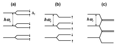
As magnetic field is tilted, the perpendicular field component, that enters the orbital effects, decreases, whereas Zeeman splitting remains constant. At a certain tilt angle , Zeeman splitting becomes equal to the half of the cyclotron splitting (see Fig. 5b), and the observed oscillation frequency doubles. This condition (so called “spin-zero”) enables to determine the spin susceptibility value for the known tilt angle as okamoto_PRL_1999 . Here , , , and are the interaction-renormalized spin susceptibility, -factor Lande and effective mass, respectively; , and – are their band values for (100) Si. This method is applicable in case of the spectrum shown in Fig. 5 a,b and cannot be applied for , i.e., for larger Zeeman splitting, as shown on Fig. 5 c.
III.3 Spin susceptibility from quantum oscillations interference in vector field
An alternative, more flexible technique for quantum oscillations measurements in magnetic field with electrically controlled magnetic field vector was implemented in Ref. cross_field . Nowadays, vector magnets are commercially available and are not rare. Magnetic field component in the plane of the 2D system produces unequal spin subband population, which is needed to determine spin susceptibility value. The normal magnetic field component is required for observing quantum oscillations related with Landau level quantization, and, hence, for counting electron population in each spin subband.
As mentioned above, the conventional way of oscillation measurements in tilted field fang_PRB_1968 ; okamoto_PRL_1999 ; zhu_PRL_2003 fails when Zeeman energy exceeds half of the cyclotron energy and further field tilting cannot decrease the Zeeman contribution gm_PRL_2002 . The “crossed-field” measurement technique with independently variable magnetic field components is free of these limitations and enables to expand the measurements range to the low density values , where Zeeman energy strongly increases due to spin susceptibility renormalization, as shown in Fig. 5 c.
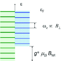
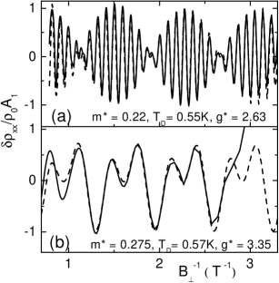
In the presence of a perpendicular field , the energy spectrum of a two-dimensional system is fully quantized and consists of equidistant Landau levels. Application of the field induces beating of the quantum oscillations, which are registered as a function of field. The cause of oscillation beating is explained on the right panel of Fig. 6: Zeeman splitting of the Landau levels induces nonequal population of the filled Landau levels in the and spin subbands.
The uppermost Landau levels in the two spin subbands vary with the field at different rates. For some field values, they cross the Fermi energy in phase and the oscillation amplitudes are summed up. For other values the Landau levels in two subbands cross out of phase and the oscillation amplitudes are subtracted. The beat frequency is proportional to the spin polarization of the 2D electron system gm_PRL_2002 :
| (10) |
where stand for the populations of the and spin subbands, respectively, is the bare value of the Lande -factor for Si, and . For the degenerate 2D Fermi gas, equation (10) may be written in a way more convenient for practical use:
| (11) |
where – is the Pauli spin susceptibility of the Fermi liquid, , and are the renormalized -factor and effective mass, correspondingly, and - Landau level filling factor. One can see that the sought for spin polarization and spin susceptibility can be found from the beating period.
Of cause, for the interacting system, the shape and amplitude of oscillations may differ from the simple Fermi liquid theory LK_JETP_1955 ; isihara-JPC_1986 ; maslov_PRB_2003 ; adamov_PRB_2006 , specifically, for the strong inter-electron interaction, for strong overlapping and mixing of the Landau levels, as well as for breakup of the Fermi surface into the multi-phase state. In particular, for the strong electron-electron interaction case, the semiclassical Lifshitz-Kosevich formula LK_JETP_1955 ; isihara-JPC_1986 is modified: the interaction effects cause temperature- and magnetic field dependent renormalization of , and adamov_PRB_2006 ; maslov_PRB_2003 ; pudalov_PRB_2014 in the exponential magnetooscillation damping factor.
These complications, however, are insignificant for the beats analysis, provided that the parameters to be determined are only beating period and oscillation phase, i.e. spin polarization, and, in the end, spin susceptibility. Accordingly, this technique enables to determine spin susceptibility of delocalized electrons possessing sufficiently large relaxation time .
III.3.1 Comment
All considered in this section techniques for measuring are based on comparison of the populations of the two spin subbands, i.e. . This certainly differs from the true thermodynamically defined quantity , considered in the next section. In case when one and the same ensemble of electrons contributes to the measured quantity and when depends linearly on field, and should coincide. Besides, the measured susceptibility value is affected by the non-ideality of the 2D system, such as finite thickness of the 2D layer tutuc_PRB_2003 ; zhang_PRB_2005 ; palo_PRL_2005 ; zhang_PRL_2005 and magnetic field dependence of the susceptibility .
IV Thermodynamic methods of measurements
IV.1 Capacitive “floating gate” method for chemical potential measurements
We consider here thermodynamic methods, based on measurements of the chemical potential and its derivative ; these measurements are sensing practically overall ensemble of charge carriers (including majority of the localized states), capable of thermalizing within time interval of the order of seconds. These methods are based on Maxwell relation for the second derivatives of the free energy :
Method of measurements of the chemical potential variations for 2D gated system was put forward in Ref. pudalov-quantosc_JETP_1985 ; in fact, it is a version of the Kelvin technique. This method was used for measuring as a function of magnetic field and electron density in a number of works pudalov_valley-split_1985 ; pudalov-osc_EF_JETPL_1986 ; krav-NDOS_physlettA_1990 ; krav_evidence_PRB_1990 .
IV.2 Electrometric measurements of the chemical potential variations
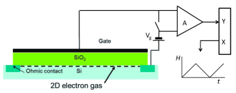
The principle of measurements is illustrated in Fig. 8. The 2D electron layer in MOS-structure is located near the Si surface and, together with the metallic gate forms a plane capacitor, spacing between the electrodes is filled with silicon dioxide. When a positive potential is applied to the gate relative the 2D layer (via one of the ohmic contacts to the 2D layer) a charge is induced in the 2D layer, with a magnitude equal to the charge on the gate but of the opposite sign.
If the voltage source is disconnected from the gate, then at low temperatures leakage currents are practically absent and the MOS structure keeps charge for sufficiently long time. Hence, the density of electrons in the 2D layer, , remains constant ( is the area of 2D layer, - the elementary charge); for the same reason remains constant also the Fermi energy (counted from the lowest size quantization level) . Here , - are the spin- and valley- degeneracy at the (100)Si surface ando-review .
When a magnetic field is applied perpendicular to the 2D plane, the energy of electrons in the two-dimensional system is fully quantized and in the absence of impurities and electron-electron interaction, the energy spectrum consists of -like discrete levels
| (12) |
where , - are the valley- and Zeeman splitting in the spectrum ando-review , - Landau level index, - cyclotron frequency, - the electron effective (band) mass in the periodic lattice potential.
Corresponding to spectrum Eq. (12), the Fermi level must have only quantized values. Taking account of the Landau level spatial degeneracy , the number of the filled levels for a given electron density is determined by the condition ( is the magnetic flux per unit area, – the magnetic flux quantum). When magnetic field varies, the Fermi level changes in a step-like fashion, jumping from the -th to the -th level. Importantly, the chemical potential changes at a constant electron density , since the gate voltage circuit is disconnected and the recharging current doesn’t flow. Such behavior of the chemical potential is considered conceptually in many textbooks on the solid state physics (abrikosov_vvedenie ; ashcroft-mermin ; kittel ) and is a prime cause of the quantum oscillations of magnetization (dHvA effect), conductivity (SdH effect) etc.
Variations in are equal to the chemical potential variations, which are detected by the electrometer in the disconnected circuit shown on the diagram of Fig. 8. In experiments pudalov-quantosc_JETP_1985 , the magnetic field was swept repeatedly in a sawtooth fashion, whereas the electrometer signal was accumulated coherently with the multichannel analyzer for signal averaging in time domain.
For accurate electrometric measurements of the potential variations, the gate potential should not change during the measurements time ( s). This sets rather strict though feasible requirements for the leakage resistance in the measurement circuit (Fig. 8): Ohm, where nF - capacitance of the gated structure pudalov_JETP_1985 .
In order to implement the “floating gate” method, on the studied surface a capacitive structure must be fabricated with a “reference” electrode, relative to which the chemical potential variations are to be measured. In Refs. pudalov_JETP_1985 ; nizhan_PRB_1994 ; goldberg_PRB_1986 , the reference electrode was made of Al film (gate), deposited on top of the oxide, above the 2D layer. Typical oscillations of the chemical potential in magnetic field are shown in Fig. 9. The magnetic field derivative of the measured signal, evidently, equals to the changes in magnetization per electron .
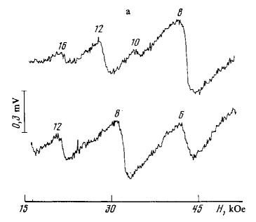
The described above method was also used in Refs. nizhan_JETP_1986 ; goldberg_PRB_1986 for detecting chemical potential variations in the gated GaAs/AlGaAs heterostructure, and in Ref. semenchin_JETPL_1985 ; pudalov_valley-split_1985 for measurements of fine details of the electron spectrum in Si-MOS structure. The attempts to measure with this technique chemical potential oscillations in the bulk crystals of Bi nizhan_JETP_1986 and Be nizhan_JETP_1985 were unsuccessful, possibly, because of the Fermi level pinning by the bulk carriers in three-dimensional crystal. For thin YBCO- and Ni-films, variations of the chemical potential with magnetic field were successfully detected in Ref. nizhan_PRB_1994 .
It is worth noting that this technique enables probing properties of electrons of the near-surface layer with thickness of the order of the Fermi wave length (in case of the 2D layer of electrons in a quantum well or in MOS structure), or of the order of the screening length - in bulk samples. A modification of the “floating gate” technique with measurements of the DC-recharging current of the MOS structure was used in Ref. pudalov-osc_EF_JETPL_1986 for measurements of the quantum oscillations of chemical potential as a function of the density of electrons in 2D layer.
IV.3 Modulation capacitive method of measuring chemical potential derivatives
In the early 2000s, the researchers interest shifted from orbital magnetization to the weaker spin magnetization effects, motivated by the issue of the potential Stoner instability in strongly correlated 2D electron system. For spin magnetization measurements, in Ref. prus_PRB_2003 an akin modulation method was developed for thermodynamic magnetization (MMTM) measurements, which was subsequently used in Refs. shashkin_PRL_2006 ; anissimova_PRL_2006 ; teneh_PRL_2012 .
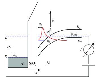
The measurements setup in MMTM method is similar to that shown in Fig. 8. However, in order to exclude orbital effects in the spin magnetization measurements, magnetic field is applied parallel, rather than perpendicular to the 2D plane. Modulation of the magnetic field at a low frequency induces modulation of the chemical potential of 2D electron layer and corresponding changes of the equilibrium charge. In contrast to the diagram of Fig. 8, here, a recharging current is measured in the capacitive structure.
The principle of measurements is explained by Fig. 10. The MOS structure is equivalent to a plane capacitor ando-review . Due to the overall sample electro-neutrality, the electron layer charge is exactly equal (with an opposite sign) to the charge on the gate electrode. When a DC voltage is applied to the gate, the free energy of the system becomes
| (13) |
where , are the free energies of the Al-gate film and the 2D layer, respectively. The typical oxide thickness nm, whereas effective “distance” of the 2D layer from the interface is nm and remains almost constant, therefore the capacitance in Eq. (13) differs only a little from the geometric capacitance of the classic capacitor, .
| (14) |
The capacitor recharging current, equals prus_PRB_2003 ; reznikov_JETPL_2010 ; teneh_PRL_2012 :
| (15) |
where is the amplitude of the magnetic field nodulation and – the capacitance of the “gate - 2D layer” capacitor, measured independently by conventional capacitance bridge. Contributions to the measured capacitance due to electron-electron interactions and finite width of the 2D layer are negligibly small reznikov_JETPL_2010 ; teneh_PRL_2012 .
The quantity is found from the measured recharging current and, due to the Maxwell relation , directly renders the desired “magnetization per electron” . The latter may be integrated with respect to to obtain the absolute value of the magnetization . The magnetic susceptibility is calculated from the slope as a function of in low fields. A DC field, applied parallel to the modulation field enables to determine the nonlinear magnetic field dependence of and .
Importantly, to the magnetization measured by this method contribute all electrons, capable of thermalizing during the field modulation period (of the 0.1 - 1 s range) note1 ; gritsenko_UFN_2009 . This difference in characteristic times (ps - in transport measurements and seconds – in thermodynamic measurements) sets a fundamental difference in the character of information, obtained from measurements with two different techniques. While in oscillatory transport measurements participate only delocalized (mobile) electrons, in thermodynamic measurements practically all electrons contribute, delocalized and localized. The latter enables to carry thermodynamic measurements even in the insulator state, where the sample resistivity raises to the GOhm range.
In Ref. reznikov_JETPL_2010 the applicability of this method was justified for measurements also in the regime of a complex capacitance, which acquires an imaginary part due to contact and channel resistances; the latter enables to expand the range of applicability of the thermodynamic method deep into the low density regime of the insulator state.
Using MMTM, in Refs. prus_PRB_2003 ; shashkin_PRL_2006 magnetization per electron was measured in high magnetic field for 2D electron system in Si. As a result, features in magnetization anticipated at field of the full spin polarization were revealed. Besides 2D electron system in Si, using this method, thermodynamic properties of electrons were measured in GaAs heterostructures tupikov_JETPL_2015 ; tupikov_NatCom_2015 and in HgTe quantum wells kuntsevich_JETPL_2020 . The main physical results of these measurements are discussed in section VI.2.2.
V Methods of local spin magnetization measurements
Need in local methods of magnetic measurements emerged in relation with discovery of a whole class of akin spin-orbit effects: the spin Hall effect (SHE), inverse spin Hall effect (ISHE), quantized spin Hall effect (QSHE), spin currents, etc. Studies in these directions are related with development of spintronics, particular, semiconductor spin logic elements, electric and optical means of the spin magnetization controlling dyakonov_Spintronics_2008 ; sinova_RMP_2015 ; zvezdin_UFN_2018 , and, more generally – with the need in effective information storage and computing devices.
The spin Hall effect reveals itself in accumulation of the spin polarization at sample boundaries when electric current flows in the bulk; importantly, oppositely directed spins are accumulated at the opposite sample edges. The idea of the spin Hall effect goes back to the anomalous Hall effect (AHE), which was observed already by E. Hall in ferromagnetic materials. In the absence of ferromagnetism, the spin-orbit interaction (SOI), the relativistic effect, also leads to the effects of spin accumulation, e.g., due to the asymmetry of carrier deflection in the scattering processes barabanov_UFN_2015 ; zvezdin_UFN_2018 . In ordinary Hall effect, Lorenz force deflects the charged carriers towards the sample edges, thus producing electric field directed perpendicular to the current. By contrast, in the anomalous Hall effect, SOI produces the force, deflecting carriers to the opposite sample edges, depending on the spin direction.
The relationship between the charge and spin currents in non-ferromagnetic materials due to spin-orbit interaction was theoretically predicted in 1971 by M. Dyakonov and V. Perel dyakonov_PL_1971 ; dyakonov_ZhETF_1971 . The idea of experiment was suggested in Ref. averkiev_FTP_1983 , and the first measurements were done in bakun_JETPL_1984 ; tkachuk_JETPL_1986 . This so called “extrinsic” SHE is related with an asymmetry of the electron scattering in the presence of SOI and is an analogue of the Mott scattering and deflection of electron beam in vacuum; its principle is schematically explained in Fig. 11. The process of charge carrier scattering by impurities includes a spin-dependent difference of the deflection probability, that causes an unbalance between oppositely directed spins.
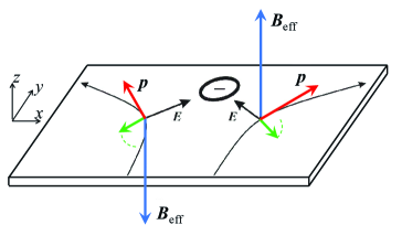
The “extrinsic” SHE was subsequently supplemented with the predicted hirsch_PRL_1999 ; zhang_PRL_2000 strong “intrinsic” SHE murakami_Science_2003 ; murakami_PRL_2004 ; sinova PRL 2004 , related with dissipationless spin currents and irrelevant to electron scattering; its physical mechanism is illustrated on Fig. 12.
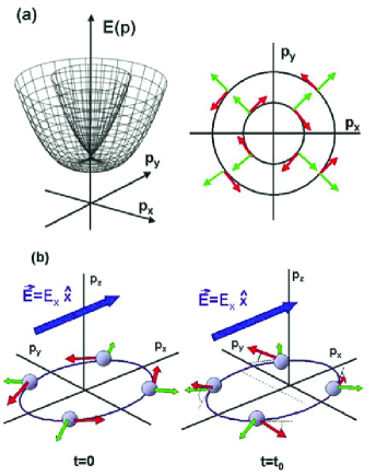
The inverse SHE (ISHE), discovered in 2006 saitoh_APL_2006 ; valenzuela_Nat_2006 ; zhao_PRL_2006 , enables electric sensing of the spin current or spin magnetization gradient. For experiments with SHE, materials are selected with high spin-orbit coupling parameters, such as GaAs ( eÅ2), ZnSe ( eÅ2), etc.
Several reviews are already published in this booming field, including sinova_RMP_2015 ; ehlert_PSS_2014 ; thanks to them, we avoid here detailed consideration of the field, and only briefly describe the physical essence of the effects, experimental techniques and the most remarkable results.
V.1 Detecting local spin polarization
V.1.1 Detecting by optical techniques
The problems in SHE detection were initially caused by lacking of measurable electric signals; for this reason the first experiments were done by optical methods kato_Science_2004 ; wunderlich_PRL_2005 ; stern_PRL_2006 . In experiments, Kerr rotation of polarization was detected (with spacial resolution) for the light transmitted through the epitaxial layers of p-GaAs, n-InGaAs kato_Science_2004 , n-GaAs matsuzaka_PRB_2009 ; sih_PRL_2006 , n-ZnSe stern_PRL_2006 , InGaN/GaN chang_PRL_2007 superlattices, etc.
The polarization rotation indicates electron spin accumulation at the sample edges, perpendicular to the applied electric field. Typical geometry of measurements is shown in Fig. 13. The beam linear polarized along was directed normally to the plane of a rectangular sample, and focuses into a spot about m in diameter. The parameter to be analyzed is the polarization rotation angle of the reflected beam; it is proportional to the spin magnetization in direction. Such setup allows detecting angle-resolved photoluminescence signal at the opposite edges of the 2D hole system. For precise sample positioning relative the incident beam in Ref. matsuzaka_PRB_2009 a precise piezo-drive was used with 1m coordinate resolution. In all measurements kato_Science_2004 ; wunderlich_PRL_2005 ; stern_PRL_2006 ; matsuzaka_PRB_2009 the Ti:sapphire laser with mode locking was used, with a typical (0.15 - 1) ps pulse duration and 76 MHz repetition rate; the wavelength 825 nm was tuned to the semiconductor absorption edge. In some experiments stern_PRL_2006 a pump-probe technique was used.
Results of the Kerr rotation measurements are shown in Fig. 13. The rotation angle corresponds to the component of the spin polarization, which diminishes with the applied in-plane external magnetic field because of spin precession. The maximum Kerr angle is reached when the external field equals the intrinsic spin magnetization ; this qualitative consideration helps to estimate the spin magnetization at edges. By taking similar measurements with uniaxially strained InGaAs sample and observing no Kerr rotation anisotropy, the authors concluded, that the observed effect in all cases was “extrinsic”, rather than “intrinsic” SHE. Analogous measurements were performed in kato_PRL_2004 in the Voigt geometry with a beam transmitted through the strained epitaxial layers of InGaAs and GaAs. In all cases the authors observed similar magnitude of the rotation angle: rad for mV/m.
The above experiments were performed in the regime of a “weak” spin-orbit coupling, i.e. when the SO- splitting is smaller than the disorder-induced level broadening. In the “strong” SO-coupling regime measurements were taken in wunderlich_PRL_2005 , where the studied 2D hole layer was a part of a p-n junction in the light emitting diode. The current flowing through the p-n junction is accompanied by electroluminescence due to electron-hole recombination. Beyond the ordinary exciton luminescence, the electroluminescence spectrum contained a circular polarized broadened line. Because of the optical selection rules, the circular polarization in a certain direction points at a spin polarization in this direction of carriers involved in the recombination.
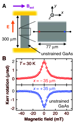
In all experiments, the Kerr angle magnitude (or the spin accumulation magnitude ), in accord with the theory, was found linear in electric field . The spin relaxation time , extracted from data approximation (e.g. in Fig. 13) was fit to a Lorentzian form ; it didn’t depend on , but was coordinate-dependent, increasing with distance from edges. At 20 K the peak value of the spin density near the edges was estimated as spins/m3 stern_PRL_2006 . Assuming a simple spin diffusion model, one can model the spin accumulation profile, related with spin current, as , where - is the spin diffusion length. From approximation of experimental data in Ref. stern_PRL_2006 , an estimate m was found for K. The spin current density along may be written as , from which spin conductivity (Ohm .
It is important to note for potential applications, that while with temperature growth the magnitude of the effect diminished (as well as the spin polarization , spin relaxation time , and spin diffusion length, the latter from m at 20 K, to m at 295 K), the effect remained pronounced even at room temperature.
V.1.2 Detecting by electrical methods
For electrical detection, set-ups with non-local geometry are used, in which spin-polarized carriers are injected from ferromagnetic to a nonmagnetic material. The detecting method is commonly based on the ISHE, where the Hall voltage is induced by spin current. Many experimental setups are described in literature valenzuela_Nature_2006 ; valenzuela_JAP_2007 ; saitoh_APL_2006 ; werake_PRL_2011 ; lou_NatPhys_2007 ; ehlert_PSS_2014 ; garlid_PRL_2010 ; brune_NatPhys_2010 , which use various nonmagnetic materials, including normal metals, superconductors, nanotubes etc.
Two different approaches are mainly used for nonlocal electric detecting of SHE: (1) detecting the “direct SHE” i.e. spin accumulation at two edges of a sample due to SOI, under flow of charge current of unpolarized carriers, and detecting spin magnetization accumulated at the edges with ferromagnetic potential contacts ehlert_PSS_2014 ; ehlert_PRB_2012 ; garlid_PRL_2010 , and (2) detecting the “inverse SHE” (ISHE) by injection of polarized charge carriers via ferromagnetic current contacts and by detecting unbalance in spin accumulation at the edges with nonmagnetic potential contacts lou_NatPhys_2007 ; olejnik_PRL_2012 ; valenzuela_APL_2004 ; choi_NatNanotech_2015 .
Schematics of nonlocal electric detection by the 2nd method (ISHE) is shown in Fig. 14). In case the charge current is spin unpolarized (Fig. 14,a), it generates spin accumulation at the sample edges (as well as in SHE), not leading to Hall voltage appearance because of the equal number of charge carriers deflects to opposite sides. However, in case the charge current is spin polarized (Fig. 14,b) by means of ferromagnetic injection with magnetization directed out of plane, the initial unbalance of electrons with spins and cause inequality of electrons, scattered to different sides. As a result, a Hall voltage arises between the Hall contacts C and D. The Hall voltage is measured non-locally, away from the injector, whereas Hall contacts and injector are disconnected galvanically in order to avoid voltages generated by ordinary Hall effect and by magnetoresistance anisotropy. Therefore, the Hall effect, induced by the spin current, shown in Fig. 14,b is the effect inverse to SHE, shown in Fig. 14,a.
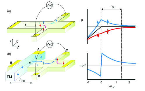
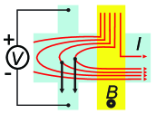
The polarized electrons are injected in the vicinity of and diffuse with equal probability towards two opposite arms of nonmagnetic material. The process of nonlocal current flow is illustrated in Fig. 15.
In the diffusion process, the nonlocal spin current decays with distance away from the injection point as valenzuela_JAP_2007
| (16) |
where is the polarization of the injected current (Fig. 14,b), – the cross-section area of the nonmagnetic strip, and is the spin diffusion length. For the geometry shown in Fig. 14,a
| (17) |
where - is the width of nonmagnetic metal strip, - Drude conductivity for the charge current and - the “spin-Hall” conductivity. Substituting Eq. (16) to the Eq. (17), one obtains non-local Hall resistance
In practical devices valenzuela_Nature_2006 CoFe was chosen as the ferromagnetic material, and Al - as a normal metal. The tunnel barrier between Al and CoFe is achieved by oxidation of the Al-strip. The presence of the tunnel barrier is essential for uniform distribution of the injected current, and also for increasing polarization of injected electrons. Typical parameters of this device , and nm for the Al- strip thickness of 12 and 25nm, respectively. The spin diffusion length sets the required strip length nm.
An elegant setup for the nonlocal ISHE detection in the double-arm H-bridge was realized in Ref. brune_NatPhys_2010 . Usually, for ISHE detecting with two-arm bridges, spin polarized carriers are injected via a ferromagnetic contact choi_NatNanotech_2015 . Unlike this, for spin polarized current injection in Ref. brune_NatPhys_2010 , a HgTe/CdHgTe heterostructure was used with HgTe quantum well thickness greater than 6.3 nm. Due to the spectrum inversion, in such structure a regime of a topological insulator is formed, where the spin polarized current flows along the edges, thereby allowing to get rid of ferromagnetic contacts.
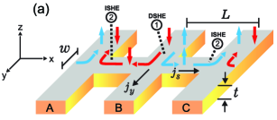
The idea of ISHE detection using the double H-bridge was suggested in Ref. hankiewicz_PRB_2004 . Such setup was used for measuring SHE in Au films mihajlovic_PRL_2009 , PbTe layers aleszkiewicz_PSS_2013 , and graphene balakrishnan_NatPhys_2013 . Principle of its operation is explained in the inset to Fig. 16. A current of unpolarized charges flows in the middle arm B. Under presence of SOI, the dominant scattering direction depends on spin; as a result, a spin current arises in perpendicular direction. Due to ISHE, carrier scattering causes charge current in the -direction, perpendicular to the current (ISHE) and a difference of potentials (or current) is induced in arms A and C. Despite the doubtless advantage of the double H-bridge, consisting in the absence of ferromagnetic contacts, the interpretation of results is hampered by the presence of side effects related with overheating of the arm B (due to Nernst -Ettingshausen effect) and diffusive transport ehlert_PSS_2014 .
The majority of the devices utilizes the extrinsic SHE, caused by the scattering anisotropy in the diffusive transport regime. The ballistic regime of intrinsic SHE brune_NatPhys_2010 ; choi_NatNanotech_2015 was realized only for materials with large carriers mean free path at low temperatures (e.g., InAs), and for devices with a short channel. Thus, in Ref. choi_NatNanotech_2015 a method was utilized for spin precession detecting under ballistic propagation of carriers, injected from the ferromagnetic contact F (Fig. 17) into the perpendicular strip of a nonmagnetic material with large SO coupling (InAs quantum well).
When carriers are injected from a contact polarized by the external field along direction, and are accelerated by an electric field to the left side into the region, then in the nonlocal ballistic regime the charge current equals to zero in the region (see Fig. 15).
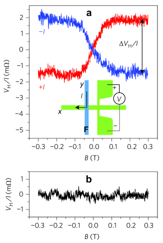
In materials with Rashba spectrum, the spins tend to align perpendicular to the electron velocity and to the “installed” electric field of the quantum well. In this picture, the spin directed initially (at ) along starts precessing as a function of coordinate . One can qualitatively think that both, the electron trajectory and Hall voltage between the strip edges will exhibit spatial oscillations datta_APL_1990 with a period , where - is the Rashba spectrum parameter. As a result, the Hall voltage shows antinodes at distance , , etc. Its sign inversion under current inversion is seen in Fig. 17a. For magnetization directed along , the carriers injected into InAs propagate ballistically with no spin precession, with no trajectory bending and the Hall voltage does not arise (Fig. 17,b).
Numerus experiments confirmed the operational capability of the described devices and the ability of electrical detecting SHE. Quantitative data were obtained on the parameters of spin diffusion: the spin diffusion length and its temperature dependence valenzuela_JAP_2007 ; ehlert_PSS_2014 .
V.2 Magnetometry based on NV-centers
The methods described in the preceding section allow for sensing electron spin magnetization with spatial resolution of the order of m. However, in some cases there is a need in studying magnetization features on a nanoscale. In magnetic materials and non-trivial magnetic phases, such as skyrmions, magnetic topological insulators, spin density waves, Abrikosov vortices in superconductors, the non-uniform magnetic structures arise at nanoscale. Negatively charged nitrogen-substituted vacancies (NV-centers) in diamond offer a possibility of sensing on the atomic scale, suitable for quantum magnetization probing with a nm-resolution.
Figure 18,a shows an NV-center in the diamond lattice, and Fig. 18,b – schematic energy levels. The NV-center in diamond consists of the substituting nitrogen atom, neighboring to the carbon vacancy. Such centers emerge in bulk and nano-crystalline diamonds: synthetic diamonds grown by CVD, as a result of radiation damage and anneal, or by ion implantation and anneal. The centers exist as negative (NV-) and neutral (NV0) charge states doherty_PhysRep_2013 . Besides diamond, the vacancy centers have been found also in silicon carbide (SiC) kraus_SciRep_2014 ; kraus_NatPhys_2014 .
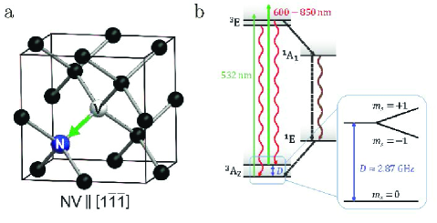
Schematics of the NV--center and energy level structure are shown in Fig. 18. The ground () and excited () states form the triplet with sublevels and . The transition may be excited in optical wavelength range 450-637nm, and the fluorescence of the transition occurs in the wavelength range 637 to 800 nm.
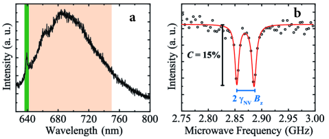
Figure 19,a shows a luminescence spectrum at room temperature fuchs_NJP_2018 . The purely electronic transitions between the excited and the ground states lead to a narrow zero-pnonon line (ZPL) at 638 nm. Beside this line, there is a wide phonon wing of lines (PSB), shifted to the red side; it contains about 96% intensity of the NV-center luminescence zhou_APL_2017 .
Optical transitions mainly occur with spin conservation, however, the spectrum contains levels crossings between the singlet and triplet states. Therefore, beside the direct transition from to , the fluorescence decay channel includes also intermediate long-living singlet states, as well as radiationless transitions from to , and from to . As a result, the relaxation rate to the state is higher, than to the state. Because of this difference, under optical pumping an optical spin polarization develops - the main part of the population transfers to the state. The fluorescence of the NV-center is spin-dependent and its level is determined by the spin polarization degree. Such dynamics of the levels population allows to polarize the electron spin of the NV-center via a non-resonant excitation (typically, at the 532 nm wavelength, by s pulses).
In the NV--center, the singlet and triplet spin sublevels and of the ground state in zero field are split by the crystal field: the energy difference is GHz (Fig. 18). Weak external magnetic field shifts the sublevels , so that their splitting varies proportionally to the field projection on the NV-center axis: MHz/Gs. Therefore, the NV--centers may be detected not only in optical transition between the ground and excited levels, but also in the microwave (MW) range, using conventional electronic paramagnetic resonance (at a frequency of 2.87 GHz in zero field), or by optically detected magnetic resonance (ODMR) oort_SSP_1988 ; taylor_NatPhys_2008 ; maze_Nat_2008 . In the latter case, the applied resonant microwave radiation transfers part of the population from , decreasing fluorescence signal, excited by non-resonant optical pumping. The properties of NV-centers are reviewed in detail in Ref. doherty_PhysRep_2013 .
Figure 19 shows an example of optical detection - optically detected magnetic resonance (ODMR) - a sharp intensity drop of the narrow luminescence line under coincidence of the microwave signal frequency with spin subleveles splitting. The unique distinction of the NV- centers from other solid state systems with single spins consists in that the long coherence time is achieved even at room temperature. Thanks to this feature, the individual NV-center in diamond crystal with low defect density may provide the threshold sensitivity as low as 30 nT/Hz1/2 maze_Nat_2008 and even 4.3 nT/Hz1/2 balasubramanian_NatMater_2009 at room temperature and in the atmospheric environment.
The second unique feature of the NV-center consists in the small volume of the sensor, practically of an atomic scale. This enables to bring the sensor to a sample at the nm-distance for visualizing magnetic field on nanoscale. Magnetic field of individual spins decays as a 3rd power of distance and were a sensor located away at mm distance, the field from the single spin would be negligibly low, Tesla. The NV-centers may be formed within 5 nm of the diamond surface, conserving at the same time long enough spin relaxation time, s ono_APL_2012 . The proximity of the NV-center to the diamond surface enables sensing magnetic field of individual spins that is in the range of T maze_Nat_2008 ; balasubramanian_NatMater_2009 ; maletinsky_NatNanotech_2012 ; kleinlein_MicroelEng_2016 ; appel_RSI_2016 .
V.2.1 Scanning microscopy based on NV-centers
Magnetic sensors with NV-centers are compatible with the scanning probe microscopy technique; owing to this circumstance they are used for magnetic field visualization at nanoscales. In the scanning magnetic NV-microscope, the diamond nano-pillar serves not only as the probe tip, but also as a nano-photonic light guide. In the latter capacity it effectively collects and guides photoluminescence signal from the NV-center to the optical registration system rondin_RepProgrPhys_2014 . Schematic arrangement of the NV-magnetometer with optical sensing is shown in Fig. 20. Theory of magnetic scanning NV-magnetometers operation and means of their optimization are considered in fuchs_NJP_2018 ; barry_RMP_2020 .
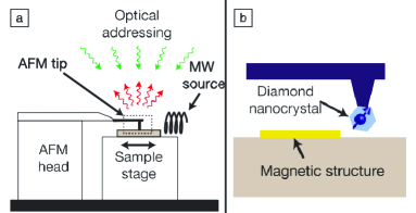
In this relatively young area, several reviews and monographs are already published jensen_book ; doherty_PhysRep_2013 ; hong_MRSBull_2013 ; fuchs_NJP_2018 ; wojciechowski_Materials_2019 ; levine_Nanophotonics_2019 ; boretti_Beilstein J. Nanotechnol_2019 ; barry_1903.08176 ; schirhagl_ARPC_2014 and PhD-dissertations nizov_thesis . Particularly, there are described various applications of the NV- magnetometry for studying ferromagnetic 50-nm grains in magnetostatic bacteria, 10-nm grains in meteorites, magneto-marked cancer cells sage_Nat_2013 ; fu_Sci_2014 ; glenn_NatMeth_2015 . Owing to the high spatial resolution and nontoxic diamond, NV-microscopes are successfully used in neuroscience and biology schirhagl_ARPC_2014 , including intracellular dynamics detecting of a living cell mcguinness_NatNano_2011 ; kuwahata_SciRep_2020 . The NV-magnetometers are expected to enable imaging of individual molecules by NMR and MRI techniques; detecting single electron spin was already demonstrated grinolds_NatPhys_2013 .
Traditional technical applications of the NV-magnetometers are the characterization of read/write magnetic heads, measurements of the stray fields from magnetic domains in hard disk drives, etc. maletinsky_NatNanotech_2012 ; jakobi_NatNanotech_2016 . In condensed-matter physics, NV-magnetometry was used for studying Meissner effect, structure of magnetic flux vortices in superconductors waxman_PRB_2014 , structure of domain walls and vortices in thin magnetic films tetienne_Sci_2014 ; rondin_NatCom_2013 , spin-wave excitations sar_NatCom_2015 , skyrmions, spin ice, and other exotic materials rondin_RepProgrPhys_2014 ; dussaux_NatCom_2015 .
V.3 Scanning probe magnetometers
Beside the considered above magnetic microscopy based on NV-centers, more traditional methods are also widely used for local magnetic surface probing.
V.3.1 Scanning magnetic force microscopes
Since the first realization of the magnetic force microscope in 1987 martin_APL_1987 a great number of MFM designs have been developed and described in detail in literature yaminskii_UHN_1999 ; martin_APL_1987 ; cordova_NanoworldJ_2016 . To date, they have become common in laboratory practice and are commercially available as an option to the atomic force microscopes (AFM) ntmdt .
The probes usually used for measurements with MFMs, are made of either magnetic materials, or with a magnetic film (Co) deposited onto an ordinary nonmagnetic probe Stiller_MeasSciTechnol_2017 . In the latter case, the stray magnetic fields in the vicinity of tip are smaller by an order of magnitude, than for the probes made of magnetic wires. In MFM measurements in static regime the probe – magnetic tip must be located away of the surface, in order the magnetic interaction forces exceeded Van der Waals forces (the dominant forces in the AFM regime). Because of this, MFMs have a limited spatial resolution. The MFM measurements usually require two cycles of scanning: at a small distance of the surface and at a large distance, with subsequent subtraction of the results for excluding contribution from Van der Waals interaction.
There are also developed bimodal MFM designs; they enable measuring the AFM and MFM signals during the single scan. For this purpose, the small amplitude (nm) mechanic oscillations are excited in the elastic console, simultaneously at two frequencies; by lock-in detecting the ac signals at two frequencies the two contributions are disentangled: from the the long-range magnetic forces (MFM), and short-range Van der Waals forces (AFM) jason_APL_2009 ; rodriguez_APL_2004 ; li_APL_2009 ; schwenk_APL_2014 ; schwenk_APL_2015 .
V.3.2 Magneto-resonant force microscopy
This method (MRFM) combines ESR and NMR methods with magnetic force microscopy sidles_APL_1991 ; sidles_RSI_1992 and, in principle, allows for 3-dimensional imaging of magnetization inside materials; several reviews on MRFM are published, e.g., sidles_RMP_1995 ; yaminskii_UHN_1999 ). As well as MFM, MRFM contains an elastic console with a probe at its end, located at a small distance from the sample. Microwave field with a frequency tuned to the magnetic resonance changes spins orientation (of electrons or nuclear) and, hence, the sample magnetization. This causes changing the magnetic force acting on the sample and shaking the elastic console. In order to improve the MRFM sensitivity, the amplitude of the microwave field is modulated at the frequency of the console mechanical resonance; thereby the amplitude of its forced vibrations is the measure of the sought for magnetization.
When the probe is scanned relative the sample, the resonant vibration amplitude (of the Angstroem scale) of the cantilever holding the sample is measured. This method is applicable for magnetic mapping with pumping either electron spins at the ESR frequency, or nuclear spins at the NMR frequency. In the earlier studies zuger_APL_1993 , a spatial resolution of m was obtained. Later on, the spatial resolution was improved up to 0.9 nm grob_Nanolet_2019 , whereas sensitivity – up to 50-100 nuclear magnetons (for the nm3 voxel) rose_PRX_2018 . Such magnetometers are now also commercially available zurich .
V.3.3 Scanning Hall microprobes
Scanning Hall magnetometers have rather simple design, can operate in the wide temperature range and in atmospheric environment; the commercially available instruments are fabricated by a number of manufacturers nano . As a Hall microprobe, semiconductor heterostructures are used with high mobility two-dimensional electron gas in GaAs/AlGaAs chang_APL_1992 , InAlSb/InAsSb/InAlSb bando_JAP_2009 , as well as Bi sandhu_JJAP and graphene sonusen_ASS_2014 . For example, in Ref. chang_APL_1992 a Hall microscope is described with a field sensitivity Gs and a spatial resolution of m, whereas Ref. dede_APL_2016 describes a vector magnetometer with a m3 GaAs-sensor, providing spatial resolution of nm.
V.3.4 Scanning SQUID magnetometers
The first scanning SQUID-magnetometer (SSM), or SQUID-microscope has been developed in 1992 black_APL_1993 . The operation principles of SQUID as the magnetic field sensor are described in detail in the textbooks clarke-book ; schmidt-book . Typical SSM design includes scanning module with a console, which carries a micro-SQUID. In contrast with MFM, where the magnetic field spatial distribution is deduced from the force acting between the probe and the sample, in SSM the magnetic field is measured with a superconducting pickup coil of the SQUID. Various designs of SSM are described in review articles kirtley_IBMJRD_1995 ; kirtley_RMS_1999 , and operation theory and data interpretation – in reith_RSI_2197 .
For achieving high spatial resolution the most suitable are the direct current SQUIDs (dc SQUIDs). Their pickup loop (m) and the SQUID sensor itself are fabricated using electron beam lithography technique. The threshold sensitivity is determined by the SQUID noise level and effective area of the pickup loop. For the typical noise level /Hz1/2 and the loop area of 7m2, the noise level is Gs/Hz1/2. In practical SSM devices vu_IEEE_1993 ; kirtley_APL_1995 , a spatial resolution of nm and the lowest detected magnetic flux /Hz1/2 was achieved for the SQUID pickup loop diameter of m.
V.4 Comparison of the local magnetometry methods
Each of the listed above local magnetometry methods has its own merits and demerits kirtley_RPP_2010 : MFM possesses high spatial resolution (up to nm) and can operate in a wide range of temperatures. The SQUID magnetometers have very high sensitivity (up to T/Hz1/2), but the worst (m) spatial resolution and are capable of working only at low temperatures. The Hall microscopes have an intermediate resolution (m). The NV-magnetometers are characterized by a good combination of the spatial resolution (nm), high magnetic sensitivity and a wide range of temperatures. For all devices, however, there is a compromise between the accessible threshold sensitivity and spatial resolution: for example, for NV-magnetometers the sensitivity raises sharply, up to pT/Hz1/2 with NV-centers ensemble (though with loss of the spatial resolution) in the mm3 volume taylor_NatPhys_2008 ; hong_MRSBull_2013 ; wolf_PRX_2015 .
VI Results of the physical investigations
In this section we briefly consider several key physical results, obtained from measurements of the electron magnetization.
VI.1 Orbital magnetization of two-dimensional electron systems
Beside the very fact of observing dHvA oscillations in the 2D electron system, in experiments stormer-dHvA_JVST_1983 ; havasoja_SSci_1984 ; eisenstein_PRL_1985 ; templeton_JAP_1988 , the theory of magnetooscillations was tested for the two-dimensional LK_JETP_1955 ; isihara-JPC_1986 ; maslov_PRB_2003 ; adamov_PRB_2006 and quasi one-dimensional wilde_PhysE_2004 systems. In Refs. meinel_PRL_1999 , electron magnetization was probed in the regime of the fractional quantum Hall effect.
Measurements of the orbital magnetization already in 1980-1990-th were used for obtaining information on the disorder induced Landau level broadening, their shape, on the density of states within the gaps between the levels, character of electron scattering potts_JPCM_1996 ; zhu_PRB_2003 ; usher09 ; ruhe_PRB_2006 ; wilde_PSS_2008 , on the spatial inhomogeneity of electron distribution and its effect on the oscillations damping shoenberg_book . Further, magnetization measurements in 2D systems were used for studying breakdown mechanisms and current “pinching” in the regime of the quantum Hall effect (QHE). The review article usher09 considers in detail the related contactless magnetic measurements for studies of the orbital magnetization and charge transport.
Orbital magnetization measurements are also commonly used for estimating the residual resistance value in the quantum Hall effect regime. The results of these measurements are briefly described in section VI.1.1. Absolute amplitude of the dHvA oscillations, inter-electron exchange interaction at neighboring Landau levels were measured using various methods of magnetometry pudalov-osc_EF_JETPL_1986 ; krav_PRB_1990 ; meinel_PRB_2001 . The results of these measurements were compared with theoretical calculation macdonald_PRB_1986 ; meinel_PRB_2001 of the oscillations amplitude enhancement due to the many-body effects of electron-electron interaction (the so called “inter Landau level interaction”).
Recently, in connection with intensive studies of quasi two-dimensional high temperature superconductors and topological insulators, measurements of the magnetization oscillations obtained even wider dissemination.
VI.1.1 Hysteresis non-stationary recharging effects in the QHE regime
With growing ratio, the diagonal components of resistivity and conductivity in the QHE regime diminish exponentially and further saturate. The residual dissipative resistivity is the important parameter both, for clarifying transport mechanism in the gapped state, and for estimation of the accuracy of reproducing the quantized Hall resistance in the Ohm standards pudalov_JETP_1985 ; krasnopolin_IET_1987 . The residual resistance, though, is so tiny, that can hardly be measured with contact-type transport techniques; besides, the area in the vicinity of the heavily doped contacts introduces an excessive electron scattering. For this reason the possibility of contactless estimation of the true residual resistance using magnetometry is very valuable.
The nonstationary effects in recharging of the two-dimensional layer in the quantum Hall effect have been found in Ref. pudalov_SSC_1984 in measurements of the chemical potential variations for Si MOS structure, and, independently, in Ref. eisenstein_APL_1985 in measurements of the magnetization oscillations in GaAs-AlGaAs heterojunction. Figure 21 shows, that the hysteresis effect in chemical potential is observed both for varying , and electron density . The phenomenological interpretation of the observed hysteresis, suggested in pudalov_SSC_1984 , was confirmed in subsequent studies, however the microscopic origin of the effect for a long time remained a subject of debates.
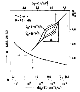
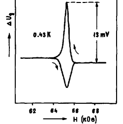
The physical picture of nonstationary eddy currents excitation at first glance is simple – under magnetic field or electron density changes, in the quantum Hall effect regime, a relationship must hold between the number of electrons and flux quanta (where – integer). This process requires recharging current to flow in the 2D layer. The Lorentz forces decline the charges coming into the 2D-layer, thereby causing eddy currents excitation. The decay time of the eddy currents tends to infinity for . In practice, however, saturates below a certain temperature; the corresponding saturation of the decay time allows to determine an important parameter – the true value of the dissipative residual resistance of the 2D system in the QHE regime, undistorted by contact effects.
The nonstationary recharging currents were studied in the integer QHE usher09 ; potts_JPCM_1996 ; faulhaber_PRB_2005 ; kershaw_NJP_2007 and fractional QHE watts_PRL_1998 regimes. Beside macroscopic 2D structures, the nonstationary eddy currents were observed also in quantum dots in the QHE regime pioro_PRB_2006 . The dynamics of eddy currents decay was measured in many works pudalov_SSC_1984 ; eisenstein_APL_1985 ; jones_SSC_1995 ; kershaw_NJP_2007 . For GaAs-AlGaAs heterojunction in Ref. eisenstein_APL_1985 the decay time was estimated as 300 s at mK. In more detailed investigation of the eddy currents decay dynamics performed at temperature 40 mK in the QHE state jones_SSC_1995 , the decay was found to be consistent with exponential function whose argument strongly varies with temperature, as expected for the hopping-type conduction in the QHE regime. However, for deeper resistance minima a more complex picture was found.
For the state, eddy currents initially decay fast, with a characteristic time s which is related with a breakdown of the QHE by eddy currents. Then, a slower process starts developing with a characteristic time h. Taking the value as an estimate of the true decay time in the low current regime, in Ref. jones_SSC_1995 an estimate was obtained for the residual resistance at mK: Ohm/ for the and Ohm/ for states. Similar estimate was obtained in Ref. pudalov_SSC_1984 for the Si-MOS structure (, K): Ohm/ and in eisenstein_PRL_1985 for the GaAs/AlGaAs heterojunction.
Thus, for a typical capacitance of 1 nF for a gated 2D structure, the characteristic recharging time lies in the range from s eisenstein_PRL_1985 to s pudalov_SSC_1984 ; jones_SSC_1995 . These figures are cited here for illustration of the time scale of the effect; of course, they depend on temperature, on the relevant energy gap in the electron spectrum and on the Landau level broadening jones_SSC_1995 .
Consequently, the giant resistance drop in the QHE regime by a factor of , illustrates an empirical accuracy of reproducing the quantized resistance value in the Ohm standards pudalov_JETP_1985 ; krasnopolin_IET_1987 . Another practical application of the sharp peaks of nonstationary magnetic response under recharging in the QHE regime is the control of homogeneity of the 2D system. Indeed, since raises exponentially sharp with deviation from the middle point between the Landau levels, the hysteresis effects occupy a narrow range in field or in density; the sharp response thereby uncovers the presence of domains with different concentration of delocalized states in the 2D layer.
Already in the first paper pudalov_SSC_1984 it was pointed that the eddy currents may flow locally, around the macroscopic localized areas in a smooth fluctuating potential landscape, or along the real sample edges, leading to a stored inductive or capacitive energy. This issue was discussed in a number of papers jones_SSC_1995 ; faulhaber_PRB_2005 , until experimentally, using an electrometer with submicron spatial resolution klaffs_PhysE_2007 ; huels_PRB_2004 , the profile of nonstationary current distribution was measured. It was found, that indeed, the eddy current is concentrated mainly along the 2D system perimeter, at a few micron distance from the 2D sample edges. This conclusion is consistent with magnitude of the eddy current estimated from direct measurements using the torque magnetometer jones_SSC_1996 .
In spite of apparently exhausting answer from the experiments with a spatial resolution, the eddy current distribution, seems to be more complex jones_SSC_1996 . The induced eddy currents circulate along the equipotential lines in the presence of potential fluctuations, forming numerous current loops with various areas. Each current loop decays at its own rate, related with its capacitance and conductivity. At the end of decay, for the remaining single loop, the decay should occur exponentially with time. These arguments usher09 though plausible, however are not fully consistent with the fact, that the exponential law was not observed in the experiments even after 24h.
Finally, the nonstationary currents were used as a valuable tool for contactless measurements of the breakdown currents in the QHE regime, of the charge and current distribution in the sample in the QHE regime, and also for estimating energy gaps in the electron spectrum jones_SSC_1996 ; matthews_PRB_2004 ; kavokin_SSC_2005 ; gething_IJMP_2004 – the issues, interesting for physics and important for the QHE metrology.
VI.1.2 Structure of the density of states in the QHE regime
Measurements of the orbital electron magnetization were used in a number of studies for clarifying the energy structure of the density of states at the Landau levels, particularly, in the gaps between the levels. According to the semiclassical theory, for the ideal 2D gas with zero width of the Landau levels, , magnetization should vary with field in saw-tooth fashion, with the amplitude per electron and with zero width of jumps in field ando-review ; kukushkin_UFN_1988 . Approximately similar dependence was observed experimentally in high mobility GaAs/AlGaAs heterojunctions wiegers_PRL_1997 ; schwarz_PRB_2002 ; wilde_PSS_2008 .
To account for disorder effect, in case of the isotropic elastic scattering and ideal non-interacting electron gas, the density of states usually is described by Gaussian or Lorentzian function usher09 ; eisenstein_PRL_1985 ; kukushkin_UFN_1988 :
| (18) |
where is the magnetic length, – energy of the -th Landau level, and – level broadening.
It is well known however, that the experimentally measured density of states deviates from the Gaussian dependence. In many papers this deviation is phenomenologically described by introducing a background density of the in-gap states schwarz_PRB_2002 between the Landau levels:
| (19) |
where the first term describes the energy independent density of states, and – is a fitting parameter.
In Refs. zhu_PRB_2003 ; schwarz_PRB_2002 ; wilde_PRB_2006 ; kuntsevich_NatCom_2015 the measured oscillations of the thermodynamic parameters for 2D electron system were compared with theory. The shape of the measured quantum oscillations in pots_JPC_1996 ; tupikov_JETPL_2015 turned out to be described in the best way using the Lorentzian distribution with field independent , and by using as an adjustable parameter. In contrast, in Ref. wilde_PRB_2006 ; schwarz_PRB_2002 , the authors successfully approximated the shape of magnetization oscillations (and in Ref. gornik_PRL_1985 – shape of the electron specific heat) by using Gaussian distribution with and with constant . Finally, in Ref. zhu_PRB_2003 , the oscillations were found to be equally well described with Gaussian and Lorentzian distributions, with field independent .
This apparent inconsistency of experimental results, in fact, finds an explanation in theoretical calculations for a smooth random potential sa-yakanit_PRB_1988 ; raikh_PRB_1993 ; according to those in weak fields the Landau level width must vary with field as , whereas in strong field must saturates and become field independent.
The empirically determined non-zero width of magnetization jumps , i.e. the non-zero “background” density of states in the QHE regime is often attributed to in-gap states, belonging to a separate reservoir of electron states, outside the 2D system. Within the framework of such approach, from the width of jump one can estimate the concentration of such states, by describing it phenomenologically with the same parameter , . In particular, in Ref. wiegers_PRL_1997 ; schwarz_PRB_2002 the authors estimated for in field of 12 T. However, such huge value schwarz_PRB_2002 ; wiegers_PRL_1997 , and even zhu_PRL_2003 , we believe, make this hypothesis unphysical.
Quite similar idea of the existence of an electron reservoir outside the 2D system, where electrons may enter and quit, depending on the Fermi level position in the gap, was discussed at the earlier stage of the QHE studies. In order to test this assumption, in Ref. pudalov-charge_JETPL_1984 measurements were performed of the charge incoming the MOS structure. It was found experimentally, that this charge coincides with the charge of the 2D layer within experimental accuracy of ; in other words, the reservoirs of such huge capacity are missing in the Si-MOS structure.
In Refs. gerhardts_PRB_1986 ; gudmundsson_PRB_1987 an attempt was performed to link the background density of states with statistical fluctuations of electron spatial distribution. Another interpretation of the puzzling background density of states was suggested in semenchin_JETPL_1985 ; pudalov-quantosc_JETP_1985 ; wang_PRB_1988 : the authors described the experimentally observed density of states using the Gaussian distribution whose width depends on the filling factor in oscillatory fashion. Such interpretation is consistent with the concept of nonlinear screening and also with experimentally observed oscillations of the Landau level width semenchin_JETPL_1985 ; pudalov-quantosc_JETP_1985 .
VI.1.3 Renormalization of the oscillation amplitude of orbital magnetization by inter-electron interaction
As described above, the energy spectrum of 2D system in quantizing perpendicular magnetic field consists of -like discrete levels (12)]. The magnetization per electron in 2D system :
| (20) |
This relationship is fulfilled in all field intervals between the integer numbers of level fillings ( – integer, – flux quantum), where the magnetization experiences jump. The amplitude of the jumps equals for cyclotron splittings (i.e. transitions ), or – for Zeeman splittings between levels with oppositely directed spins.
Non-zero temperature broadens the step-like changes of the filling function at the Fermi level, that leads to broadening of the interval of the of jump-like changes in . Disorder, in its turn, causes broadening of the initially -like Landau energy levels. As a result, both factors, temperature and disorder, cause diminishing of the jumps amplitude .
When interaction is taken into account, the effective mass and g-factor vary due to the Fermi-liquid renormalization, and the jumps amplitude must differ from the free electron value. In quantizing magnetic field the renormalization (for the account of the so called “inter Landau levels interaction” or “level repulsion”) leads to the enhancement in the jump amplitude. Such enhancement of the energy level splitting in the interacting 2D electron system was observed experimentally and predicted theoretically macdonald_PRB_1986 .
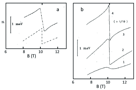
Figure 22a shows the measured chemical potential for 2D electron system in Si as a function of perpendicular magnetic field (the upper curve) krav-NDOS_physlettA_1990 ; krav_PRB_1990 . The sharp jump at about 10 T corresponds to the Fermi level transition from the 2nd to the 3rd energy level. For the Fermi level location in the energy gap, i.e. in the integer QHE regime, as was described above, resistance of the 2D system decays exponentially strong, its recharging under such conditions is accompanied by eddy currents excitation, considered in section VI.1.1. For this reason, the behavior in Fig. 22 in this range of fields is schematically interpolated with a dash-dotted line.
Figure 22b shows the dependence krav-NDOS_physlettA_1990 , calculated for the non-interacting 2D electron gas at in the absence of disorder, and also for a typical disorder-induced Landau level broadening. One can see, the slope of the measured dependence (i.e. magnetization per electron) for is about a factor of two greater than the maximum possible slope, (), for the non-interacting electron gas. The enhanced slope originates from the contribution of electron-electron interaction, that also enters the inverse thermodynamic density of states (thermodynamic compressibility) and causes its negative value. The latter effect was predicted by Efros efros88 and experimentally observed in Refs. krav-NDOS_PLA_1989 ; krav-NDOS_physlettA_1990 ; eisenstein_PRB_1992 .
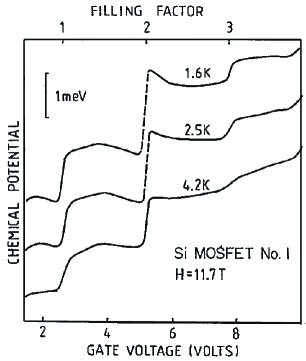
Qualitatively, the “negative compressibility” is clearly seen also in Fig. 23, where the chemical potential for two-dimensional electron system is shown versus electron concentration, measured in constant magnetic field krav_PRB_1990 . Instead of the anticipated (for non-interacting system) step-like dependence with jumps and with the related positive slope in the interval between them, one can clearly see intervals with . These wings with negative slope on both sides of the integer fillings are the direct evidence for the negative contribution to the chemical potential due to the inter-electron interaction (i.e., negative compressibility). The renormalized amplitude of the dHvA oscillations was measured in a number of works meinel_PRB_2001 and was found to be in a qualitative agreement with theory.
VI.2 Spin magnetization of electrons
The problem of the electron spin magnetization measurements in 2D systems became topical in 2000s, in connection with investigations of the inter-electron correlation effects. The many body effects become progressively stronger in 2D systems under decreasing electron concentration; the latter, in its turn, became possible as a result of the improvement in the quality of 2D structures. Commonly, the inter-electron interaction is quantitatively characterized by a dimensionless ratio of the potential interaction energy and the kinetic Fermi energy, ando-review .
In order to study the effect of electron-electron correlations on the spin degree of freedom, numerous experiments were performed, using direct thermodynamic methods, as well as indirect (i.e. based on theoretical models) transport methods; their brief description and the major results are given below.
VI.2.1 Spin susceptibility renormalization, determined from oscillatory and monotonic transport
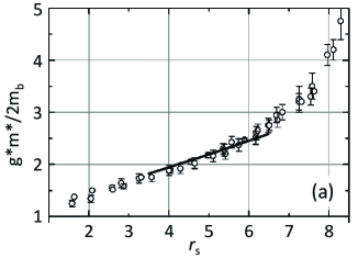
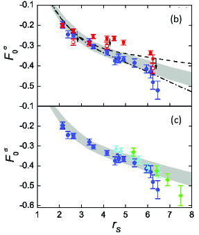
Figure 24 shows the main result, summarizing measurements of for 2D electron system in Si-MOS structures fang_PRB_1968 ; okamoto_PRL_1999 ; gm_PRL_2002 ; zhu_PRL_2003 . One can see that, as a result of electron-electron interaction, the susceptibility increases monotonically with (i.e. with density lowering) by a factor of , though remains finite.
From the measurements of together with the renormalized effective mass , one can extract the renormalized Lande -factor and, hence, to estimate the lowest order Fermi liquid coupling parameter . The effective mass value may be found from temperature dependence of quantum oscillations. Fig. 24b shows the resulting dependence, obtained from quantum oscillations; the results of Ref. zhu_PRL_2003 also agree with the data in Fig. 24b. As can be seen from Fig. 24c, the -values deduced from SdH oscillations reasonably agree with the results, obtained from fitting temperature dependence by the method, considered above in Section III.1.2.
Finally, Fig. 25 from Ref. clarke_NatPhys_2007 summarizes the results for 2D electron and hole systems; it demonstrates the impact of the character of disorder, clearly breaking the data into two groups, for the short-range and long-range (as compared with the Fermi wave length Å) potential fluctuations, which are described by theories ZNA_PRB_2001 and gornyi_PRB_2004 ; gornyi_PRL_2003 , respectively.
For higher values, tends to saturation at the level of ; as a result, the Stoner instability expected for , appears to be unattainable for all studied 2D material systems. Another cause of the attainability of the magnetic transition in single-phase 2D system is discussed in Section VI.2.2.
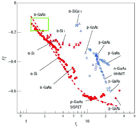
VI.2.2 Spin magnetization and susceptibility from thermodynamic measurements
The method of thermodynamic measurements was described above in Section IV.3. Using this method, and by modulating the perpendicular , rather than parallel magnetic field, in Ref. anissimova_PRL_2006 the renormalized -factor and cyclotron mass was measured for 2D electron system in Si; evidently, the results include orbital effects of inter-electron interaction. For probing purely spin effects, free of orbital contribution, measurements in Ref. prus_PRB_2003 ; shashkin_PRL_2006 were performed in magnetic field aligned strictly parallel to the 2D plane. These results taken in strong magnetic field enable to detect features, expected for the full spin polarization (see Fig. 26).
In a partially polarized system, the electrons at the Fermi level have equal density of states for both spin projection and contribute almost zero to the magnetization . Starting from the field of complete spin polarization, the value should sharply raise from 0 to , as schematically shown by a bold dashed line in Fig. 26a. A qualitatively similar behavior was observed in experiments prus_PRB_2003 ; shashkin_PRL_2006 ; dolgopolov_UFN_2019 and is shown in Fig. 26a.
Most of the measurements with this technique was performed in prus_PRB_2003 ; shashkin_PRL_2006 in the regime of strong fields , which evidently “cuts-off” the temperature dependence. In the subsequent thermodynamic measurements teneh_PRL_2012 , performed with improved sensitivity, a different behavior of was observed in weak fields (), as shown in Fig. 26b.
Here, at high electron densities, is negative teneh_PRL_2012 , as expected for the Fermi-liquid because of effective mass renormalization . At low densities becomes positive and in all cases is much greater than that expected for the Pauli spin susceptibility. When field increases (remaining all the way smaller than temperature), sharply raises and, at low temperatures, exceeds Bohr magneton more than by a factor of two (Fig. 26b).
Such behavior of is reminiscent of the dependence, anticipated for the free spins, , where is the dimensionless magnetic field. However, the fact, that exceeds Bohr magneton, points at a ferromagnetic ordering of the electron spins. The magnetization curves (Fig. 26b) saturate in field of , signalling that, the particles, which respond to the field modulation, have spin equal , rather than (1/2).
Thus, the results of Ref. teneh_PRL_2012 evidence for the emergence of a two-phase state in 2D system, consisting of paramagnetic Fermi liquid and ferromagnetic domains (so called “spin droplets”) with a total spin , comprising electrons. It seems likely, the formation of a two-phase state is more favorable, than transition to the uniform ferromagnetic state, that is in addition forbidden by the Mermin-Wagner theorem at . In the considered case, the easily orientable “nanomagnets” remain persisting as the minority phase in the majority Fermi-liquid phase even though the dimensionless conductance of the 2D system . Such conductance was commonly considered as a criterion of the well-defined Fermi-liquid state. We note, that the two-phase state often occurs in interacting electron systems in the vicinity of phase transitions, expected for a uniform state gorbatsevich_1994 ; kornilov_PRB_2004 ; gerasimenko_PRB_2014 .
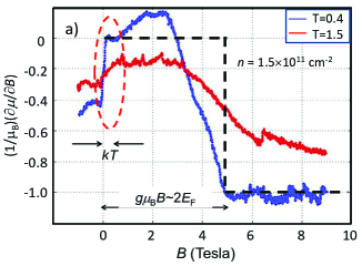
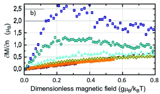
VII Conclusion
Magnetic properties measurements of non-magnetic or weakly-magnetic materials always represented a topical task, relevant for both practical material applications, and physical studies. The doubtless advantage of magnetometry is related with thermodynamic character of measurements, that in many cases, provides related simple and reliable interpretation of the results. Experimental methods of the magnetic measurements are continuously improved, mostly since the end of the previous century. This review considers various methods of magnetometry and their evolution in the last 50 years. As a result of their development, dozens of outstanding laboratory magnetometer designs appeared, followed by a large number of commercially available magnetometers and susceptometers.
The demand in magnetic measurements raised sharply in the beginning of 1970s, related with discovery and intensive studies of low-dimensional systems of electrons in the semiconductor structures ando-review and in organic crystals lebed-book ; kornilov_PRB_2004 ; kornilov_PRB_2002 . Low -dimensional electron systems manifest a rich novel physics in strong magnetic fields. Beside the traditional transport and optical measurements, their studies require also thermodynamic, and particularly, magnetic measurements. Investigations of orbital magnetization of low-dimensional electron systems and nanostructures with low number of electrons has required improving traditional designs and developing novel methods for magnetic measurements. Along with discovery and studies of the integer and fractional quantum Hall effects, simultaneously performed magnetic measurements with 2D electron systems has led to a deeper understanding of the origin of these effects, properties of novel quasiparticles, describing the fractional charge states, composite quasiparticles, consisting of electrons and flux quanta, and collective spin excitations in the electron systems.
In the beginning of the 21st century, the problem of a weaker effects of electron spin magnetization came to the forefront. This is related with the topical problem of understanding properties of strongly correlated electron systems, searching novel states of electron matter, studying effects of spin ordering and their interplay with superconducting paring, as well as with application in spintronics and quantum computations.
And at last, in recent years there were developed new methods of magnetometry with spatial and temporal resolution. Local probing uses such tools as scanning magnetometers based on the NV-centers, SQUID-magnetometers, scanning Hall magnetometers, and scanning atomic force microscopes. The time resolved magnetometry enables studying magnetization dynamics during relaxation of the system between two quantum states. These methods have great perspectives, because they are suited to magnetic measurements with more and more popular nanomaterials, nanostructures of topologically non-trivial matter, and optically controlled matter. The magnetometry methods with nm-spatial resolution and temporal resolution are now quickly developing, adapting to novel tasks and will promote novel discoveries, and accumulation of novel knowledge, particularly in such topical areas as studies of the quantum topological effects, novel quasiparticles (including, e.g. Majorana fermions), living cells, microorganisms and neuro-systems. Scanning magnetic local microscopy here suggests a unique possibility of non-invasive probing and visualization of the structure and dynamics of nano-objects.
VIII Acknowledgements
The authors is grateful to M.E. Gershenson, E.M. Dizhur, G. Bauer, G. Brunthaler, N. Klimov, H. Kojima, S.V. Kravchenko, A.Yu. Kuntsevich, L.A. Morgun, M. Reznikov, D. Rinberg, S.G. Semenchnisky, N. Teneh, and V.S. Edel’man, for fruitful collaboration in developing experimental methods, performing measurements, discussing the results, and writing the original papers. Financial support from RFBR #18-02-01013 is acknowledged.
References
- (1) Griessen R Cryogenics 13(6) 375 (1973)
- (2) Vandrkooy J, Phys. E. 2 718 (1969)
- (3) Foner S, Rev. Sci. Instr. 30 548 (1959)
- (4) Usher A, Elliott M, J.Phys.: Cond.Matter 21 103202 (2009)
- (5) Chechernikov V I, “Magnetic measurements”, Ed. by E.I. Kondorskii, MSU publishing. Moscow 1969
- (6) Eisenstein J P, Appl. Phys. Lett. 46, 695 (1985)
- (7) Eisenstein J P, H. L. Stormer, V. Narayanamurti, A. Y. Cho, A. C. Gossard, and C. W. Tu, Phys. Rev. Lett. 55, 875 (1985).
- (8) Templeton I M, J. Appl. Phys. 64, 3570 (1988)
- (9) Jones C L, Usher A, Cheng T S, Foxon C T, Sol. St. Commun. 95, 409 (1995)
- (10) Matthews A J, K. V. Kavokin, A. Usher, M. E. Portnoi, M. Zhu, J. D. Gething, M. Elliott, W. G. Herrenden-Harker, K. Phillips, D. A. Ritchie, M. Y. Simmons, C. B. Sorensen, O. P. Hansen, O. A. Mironov, M. Myronov, D. R. Leadley, and M. Henini, Phys. Rev. B 70, 075317 (2004)
- (11) Matthews A J, A. Usher, and C. D. H. Williams, Rev. Sci. Instrum., 75, 2672 (2004).
- (12) Wiegers S A J, A. S. van Steenbergen, M. E. Jeuken, M. Bravin, P. E. Wolf, G. Remenyi, J. A. A. J. Perenboom and J. C. Maan, Rev. Sci. Instr. 69, 2369 (1998)
- (13) Wiegers S A J, M. Specht, L. P. Lévy, M. Y. Simmons, D. A. Ritchie, A. Cavanna, B. Etienne, G. Martinez, and P. Wyder, Phys. Rev. Lett. 79, 3238 (1997)
- (14) Scaaphman M R, P. C. M. Christianen, J. C. Maan, D. Reuter, and A. D. Wieck, Appl. Phys. Lett. 81, 1041 (2002)
- (15) Bominaar-Silkens I M A, M. R. Schaapman, U. Zeitler, P. C. M. Christianen, J. C. Maan, D Reuter, A. D. Wieck, D. Schuh, M. Bichler, New J. of Phys. 8, 315 (2006)
- (16) Schaapman M R, U. Zeitler, P. C. M. Christianen, J. C. Maan, D. Reuter, A. D. Wieck, D. Schuh, and M. Bichler, Phys. Rev. B 68, 193308 (2003)
- (17) Pudalov V M, Semenchinskii S G, Instr. Exper. Techn. 21, 1065 (1978)]
- (18) Pudalov V M, Semenchinsky S G, J. de Physique, C6, 39, 1199 (1978)
- (19) Naughton M J, J.P. Ulmet, A. Narjis, S. Askenazy, M.V. Chaparala, R. Richter, Physica B, 246-247, 125 (1998)
- (20) Wilde M A, M. Rhode, Ch. Heyn, D. Heitmann, and D. Grundler, U. Zeitler, F. Schäffler, Phys. Rev. B, 72, 165429 (2005)
- (21) Harris J G E, D. D. Awschalom, F. Matsukura, H. Ohno, K. D. Maranowski and A. C. Gossard, Appl. Phys. Lett., 75, 1140 (1999)
- (22) Schwarz M P, D. Grundler, I. Meinel, Ch. Heyn, and D. Heitmann, Appl. Phys. Lett. 76, 3564 (2000)
- (23) Schwarz M P, M. A. Wilde, S. Groth, D. Grundler, Ch. Heyn, and D. Heitmann, Phys. Rev. B 65, 245315 (2002)
- (24) Wilde M A, M. P. Schwarz, Ch. Heyn, D. Heitmann, D. Grundler, D. Reuter, A. D. Wieck, Phys. Rev. B 73, 125325 (2006)
- (25) Knobel R, N. Samarth, J. G. E. Harris, and D. D. Awschalom, Phys. Rev. B 65, 235327 (2002)
- (26) Harris J G E, R. Knobel, K. D. Maranowski, A. C. Gossard, N. Samarth, D. D. Awschalom, Phys. Rev. Lett. 86, 4644 (2001)
- (27) Ruhe N, J. I. Springborn, Ch. Heyn, M. A. Wilde, D. Grundler, Phys. Rev. B 74, 235326 (2006)
- (28) Foner S, Rev. Sci. Instrum. 27, 548 (1956)
- (29) Foner S, J. Appl. Phys. 79, 4740 (1996)
- (30) N. F. Oliveira Jr., S. Foner, Rev. Sci. Instrum. 43, 37 (1972)
- (31) Mangum B W, Thornton D D, Rev. Sci. Instrum. 41 17646 (1970)
- (32) Bindilatti V, E. ter Haar, A. R. Rodrigues, N. F. Oliveira, Jr., G.Frassati, Physica B 194 - 196, 37 (1994)
- (33) Guertin R P, in: High-Pressure and Low-temperature Physics, ed. by C. W. Chu and J. A. Woollam, (Plenum, New York, 1978), p.97
- (34) Guertin R P, Foner S, Missell F P, Phys. Rev. Lett. 37, 529 (1976)
- (35) Reeves R, J. Phys. E: Sci. Instrum. 5, 547 (1972)
- (36) Springford M, Stockton J R, Wampler W R, J. Phys. E: Sci. Instrum. 4 1036 (1971)
- (37) Johansson T, Nielsen K G, J. Phys. E: Sci. Instrum. 9, 852 (1976)
- (38) Hoon S R, Willcock S N M J. Phys. E: Sci. Instrum. 21, 772 (1988)
- (39) Nizhankovskii V I, Lugansky L B Meas. Sci. Technol. 18, 1533 (2007)
- (40) Ausserlechner U, Steiner W, Kasperkovitz P Meas. Sci. Technol. 7, 1574 (1996)
- (41) Braggt E E, and Seehrac M S J. of Physics E: Sci. Instrum 9, 216 (1976)
- (42) Pudalov V M, Khaikin M S, ZhETF, 67, 2260 (1974)[JETP, 40, 1121 (1974)]; Pudalov V M Pis’ma v ZhETF 19, 466 (1974)[JETP Lett., 19, 250 (1974)]
- (43) See: http://www.cryogenic.co.uk
- (44) Störmer H L, T. Haavasoja, V. Narayanamurti, F. C. Gossard, W. Wiegmann, J. Vac. Sci. Technol. B 1 423 (1983)
- (45) Havasoja T, H.L. Störmer, D.J. Bishop, V. Narayanamurti, Surface Sci., 142, 294 (1984)
- (46) Meinel I, T. Hengstmann, D. Grundler, D. Heitmann, W. Wegscheider, and M. Bichler Phys. Rev. Lett. 82, 819 (1999)
- (47) Meinel I, D. Grundler, S. Bargstädt-Franke, C. Heyn, D. Heitmann, B. David, Appl. Phys. Lett. 70, 3305 (1997)
- (48) Fang F F, and Stiles P J Phys. Rev. B 28, 6992 (1983)
- (49) Pudalov V M, Semenchinsky S G, Edel’man V S Sol. State Commun. 51, 713 (1984)
- (50) Shoenberg D, Canadian Journ. Phys. 46, 1915 (1968). Shoenberg D, Templeton I M, ibid 46, 1925 (1968)
- (51) Pippard A B, in: The Physics of Metals. I. Electrons, J.M. Ziman Ed., (Cambridge university Press, 1969)
- (52) Lifshitz I M, Kosevich A M ZhETF 29, 730 (1956); [JETP 2, 636 (1956)]
- (53) Isihara A, Smrka L, J. Phys. C: Solid State Phys. 19, 6777 (1986)
- (54) Das Sarma S, and Hwang E H Phys. Rev. B 72, 035311 (2005)
- (55) Gold A V, Dolgopolov V T, Pis’ma v ZhETF, 71, 42 (2000); [JETP Lett. 71, 27 (2000)]
- (56) Shashkin A A, S.V. Kravchenko, V. T. Dolgopolov, T. M. Klapwijk, Phys. Rev. Lett. 87, 086801 (2001)
- (57) Pudalov V M, G. Brunthaler, A. Prinz, and G. Bauer, Phys. Rev. Lett. 88, 076401 (2002)
- (58) Broto J M, M. Goiran, and H. Rakoto, A. Gold, V. T. Dolgopolov, Phys. Rev. B 67 161304 (2003)
- (59) Tutuc E, Melinte S, Shayegan M, Phys. Rev. Lett. 88, 036805 (2002)
- (60) Gao X P, G. S. Boebinger, A. P. Mills, Jr., A. P. Ramirez, L. N. Pfeiffer, and K. W. West, Phys. Rev. B 73, 241315 (2006)
- (61) Lu T M, L. Sun, D. C. Tsui, and S. Lyon, W. Pan, M. Mühlberger, F. Schäffler, J. Liu, and Y. H. Xie, Phys. Rev. B 78, 233309 (2008)
- (62) Altshuler B L, Aronov A G, Zyuzin A Yu, Pis’ma v ZhETF 35, 15 (1982); [JETP Lett. 35, 16 (1982)]
- (63) Zhang Y, Das S, Phys. Rev. Lett. 96, 196602 (2006)
- (64) Vitkalov S A, Sarachik M P, Klapwijk T M Phys. Rev. B 65, 201106 (2002)
- (65) Sarachik M P, Vitkalov S A J. Phys Soc. Jpn. 72 Suppl. A, 53 (2003)
- (66) Zala G, Narozhny B N, Aleiner I L, Phys. Rev. B 64, 214204 (2001); 65, 020201(R) (2001)
- (67) Vitkalov S A, K. James, B. N. Narozhny, M. P. Sarachik, and T.M. Klapwijk, Phys. Rev. B 67, 113310 (2003)
- (68) Klimov N N, D. A. Knyazev, O. E. Omel’yanovskii, V. M. Pudalov, H. Kojima, M. E. Gershenson, Phys. Rev. B 78, 195308 (2008)
- (69) Pudalov V M, M.E. Gershenson, H. Kojima, G. Brunthaler, and G. Bauer, Phys. Rev. Lett. 91, 126403 (2003)
- (70) Shashkin A A, S. V. Kravchenko, V. T. Dolgopolov, and T. M.Klapwijk, Phys. Rev. B 66, 073303 (2002)
- (71) Proskuryakov Y Y, A. K. Savchenko, S. S. Safonov, M. Pepper, M. Y. Simmons, and D. A. Ritchie, Phys. Rev. Lett. 89, 076406 (2002)
- (72) Kvon Z D, O. Estibals, G. M. Gusev, J. C. Portal, Phys. Rev. B 65, 161304 (2002)
- (73) Olshanetsky E B, V. Renard, Z. D. Kvon, J. C. Portal, N. J. Woods, J. Zhang, and J. J. Harris, Phys. Rev. B 68, 085304 (2003)
- (74) Noh H, M. P. Lilly, D. C. Tsui, J. A. Simmons, L. N. Pfeiffer, and K. W. West, J. Phys Soc. Jpn., Suppl. A 72, 137 (2003)
- (75) Noh H, M. P. Lilly, D. C. Tsui, J. A. Simmons, E. H. Hwang, S. Das Sarma, L. N. Pfeiffer, and K. W. West, Phys. Rev. B 68, 165308 (2003)
- (76) Savchenko A K, Y.Y. Proskuryakov, S.S. Safonov, L. Li, M. Pepper, M.Y. Simmons, D.A. Ritchie, E.H. Linfeld, Z.D. Kvon, Physica E 22, 218 (2004)
- (77) Li L, S.S. Safonov, Y.Y. Proskuryakov, A.K. Savchenko, M. Pepper, M.Y. Simmons, E.H. Linfield, and D.A. Ritchie, J. Phys Soc. Jpn. 72, Suppl. A, 63 (2003)
- (78) Coleridge P T, Sachrajda A S, Zawadzki P Phys. Rev. B 65, 125328 (2002)
- (79) Gornyi I V, Mirlin A D, Phys. Rev. B 69, 045313 (2004)
- (80) Gornyi I V, Mirlin A D Phys. Rev. Lett. 90, 076801 (2003)
- (81) Clarke W R, C. E. Yasin, A. R. Hamilton, A. P. Micolich, M. Y. Simmons, K. Muraki, Y. Hirayama, M. Pepper, D. A. Ritchie, Nat. Phys. 4, 55 (2007)
- (82) Morgun L A, Kuntsevich A Yu, Pudalov V M Phys. Rev. B 93, 235145 (2016)
- (83) Li L, Y.Y. Proskuryakov, A. K. Savchenko, E. H. Linfield, and D. A. Ritchie, Phys. Rev. Lett. 90, 076802 (2003)
- (84) Kuntsevich A Yu, Morgun L A, Pudalov V M Phys. Rev. B 87, 205406 (2013)
- (85) Pudalov V M, Morgun L A, Kuntsevich A Y J. Supercond. Nov. Magn. 30, 783 (2017)
- (86) Fang F F, Stiles P J Phys. Rev. 174, 823 (1968)
- (87) Okamoto T, K. Hosoya, S. Kawaji, and A. Yagi, Phys. Rev. Lett. 82, 3875 (1999)
- (88) Zhu J, H. L. Stormer, L. N. Pfeiffer, K.W. Baldwin, and K.W.West, Phys. Rev. Lett. 90, 056805 (2003)
- (89) Tsukazaki A, A. Ohtomo, M. Kawasaki, Akasaka, H. Yuji, K. Tamura, K. Nakahara, T. Tanabe, A. Kamisawa, T. Gokmen, J. Shabani, and M. Shayegan, Phys. Rev. B 78, 233308 (2008)
- (90) Gershenson M, V.M. Pudalov, H. Kojima, N. Butch, G. Bauer, G. Brunthaler, A. Prinz, Physica E, 12, 585 (2002)
- (91) Pudalov V M, M. E. Gershenson, H. Kojima, N. Butch, E. M. Dizhur, G. Brunthaler, A. Prinz, and G. Bauer, Phys. Rev. Lett. 88, 196404 (2002)
- (92) Martin G W, Maslov D L, Reizer M Yu Phys. Rev. B 68, 241309 (2003)
- (93) Adamov Y, Gornyi I V, Mirlin A D, Phys. Rev. B 73, 045426 (2006)
- (94) Pudalov V M, Gershenson M E, Kojima H, Phys. Rev. B 90, 075147 (2014)
- (95) Zhang Y, Das Sarma S, Phys. Rev. B 72, 075308 (2005)
- (96) Zhang Y, Das Sarma S Phys. Rev. Lett. 97, 039701 (2005)
- (97) De Palo S, M. Botti, S. Moroni, G. Senatore, Phys. Rev. Lett. 94, 226405 (2005)
- (98) Tutuc E, S. Melinte, E. P. De Poortere, M. Shayegan, Phys. Rev. B 67, 241309 (2003)
- (99) Pudalov V M, Semenchinskii S G, Edel’man V S, ZhETF 89, 1870 (1985). [JETP 62, 1079 (1985)]
- (100) Pudalov V M, Semenchinckii S G, Edel’man V S, Pis’ma v ZhETF 41, 225 (1985); [JETP Lett. 41, 325 (1985)]
- (101) Pudalov V M, Semenchinsky S G, Pis’ma v ZhETF, 44, 526 (1986);[JETP Lett. 44, 677 (1986)]
- (102) Kravchenko S V, Pudalov V M, Rinberg D A, Semenchinsky S G, Phys. Lett. A 146, 535 (1990)
- (103) Kravchenko S V, Rinberg D A, Semenchinsky S G, Pudalov V M, Phys. Rev.B 42, 3741 (1990)
- (104) Ando T, Fowler A, Stern F, Rev. Mod. Phys. 54, 437 (1982)
- (105) Abrikosov A A, Introduction to the theory of normal metals, Academic Press, New York, 1972
- (106) Ashcroft N W, Mermin N D Solid State Physics, Holt, Rinehart and Winston, 1976
- (107) Kittel C, Quantum Theory of Solids, John Willey & Sons, Inc. 1963
- (108) Pudalov V M, Semenchinsky S G, Kopchikov A N, Vernikov A N, Pzinich L M, ZhETF, 89, 1094 (1985). [JETP 62, 630 (1986)]
- (109) Nizhankovskii V I, Zybtsev S G, Phys. Rev. B 50, 1111 (1994)
- (110) Zeller R T, B. B. Goldberg, P. J. Stiles, F. F. Fang, S. L. Wright, Phys. Rev. B 33, 1529(R) (1986)
- (111) Nizhankovskii V I, V. G. Mokerov, B.K. Medvedev, Yu. U. Shaldin, ZhETF 90, 1326 (1986). [Sov. Phys. JETP 63, 776 (1986)]
- (112) Semenchinskii S G, Pis’ma v ZhETF 41, 497 (1985); [JETP Lett. 41, 605 (1985)]
- (113) Alekseevskii N E, and Nizhankovskii V I, ZhETF 88, 1771 (1985). [Sov. Phys. JETP 61, 1051 (1985)]
- (114) Prus O, Yaish Y, Reznikov M, Sivan U, and Pudalov V Phys. Rev. B 67, 205407 (2003)
- (115) A. A. Shashkin, S. Anissimova, M. R. Sakr, S. V. Kravchenko, V. T. Dolgopolov, and T.M.Klapwijk, Phys. Rev. Lett. 96, 036403 (2006)
- (116) Anissimova S, A. Venkatesan, A. A. Shashkin, M. R. Sakr, S. V. Kravchenko, T.M. Klapwijk, Phys. Rev. Lett. 96, 046409 (2006)
- (117) Teneh N, Kuntsevich A Yu, Pudalov V M, and Reznikov M, Phys. Rev. Lett. 109, 226403 (2012)
- (118) Reznikov M, Kuntsevich A Yu, Teneh N, Pudalov V M, Pis’ma v ZhETF 92, 518 (2010); [JETP Lett. 92, 470 (2010)]
- (119) The SiO2/Si interface is a disordered intermediate SiOx layer, a few atomic layers thick, where the broken bonds are saturated with hydrogen in the process of the Si-MOS structure fabrication ando-review ; gritsenko_UFN_2009 . The localized states formed at the interface contribute to the threshold voltage in the relationship between the density of mobile carriers and the voltage applied at the gate of MOS structure . For the studied high mobility Si-MOS structures, the density of these localized interface states is /cm2; at low temperatures they are not recharging during many years, providing a possibility of peforming electrometeric measurements of chemical potential. The neutral interface dipoles contribute to potential fluctuations in 2D layer and to shallow electron localized states. The latter don’t perticipate in charge transport, however are thermalilizing and recharging over ms-times; therefore, they contribute to MTDM measurements prus_PRB_2003 ; reznikov_JETPL_2010 ; teneh_PRL_2012 .
- (120) Gritsenko A V, Uspekhi Fiz. Nauk 179(9), 921 (2009) [Phys. Usp., 52, 869 (2009)].
- (121) Tupikov Y, Kuntsevich A Yu, Pudalov V M, Burmistrov I S, Pis’ma v ZhETF 101, 131 (2015). [JETP Lett. 101, 125 (2015)]
- (122) Kuntsevich A Yu, Tupikov Y V, Pudalov V M, Burmistrov I S Nature Commun. 6, 7298 (2015)
- (123) Kuntsevich A Yu, Tupikov Yu V, Dvoretsky S A, Mikhailov N N, Reznikov M, Pis’ma v ZhETF 111, 750 (2020); [JETP Lett. 111 (2020)]
- (124) Dyakonov M I Spin Hall Effect, in: Spintronics, ed. by M. Razeghi, H.-J. M. Drouhin, J.-E. Wegrowe, Proc. of SPIE 7036, 70360R, (2008); doi:10.1117/12.798110
- (125) Sinova J, O. Valenzuela, J. Wunderlich, C. H. Back, T. Jungwirth, Rev. Mod. Phys. 87, 1213 (2015)
- (126) Zvezdin A K, Davydova M D, Zvezdin K A Uspekhi Fiz. Nauk 188, 1238 (2018); [Phys. Usp. 61 1127 (2018)]
- (127) Barabanov A F, Kagan Yu M, Maksimov L A, Mikheyenkov A V, Khabarova T V Uspekhi Fiz. Nauk 185, 479 (2015); [Phys. Usp. 58, 446 (2015)]
- (128) Dyakonov M, Perel V I Phys. Lett. 35A, 459 (1971)
- (129) Dyakonov M I, Perel V I Pis’ma v ZhETF 13, 657 (1971); [JETP Letters 13 467 (1971)]
- (130) Averkiev N S, Dyakonov M I, Fiz. Tekhn. Semicond., 17, 629 (1983); [Sov. Phys. Semicond. 17, 393 (1983)]
- (131) Bakun A A, B.P. Zakharchenya, A.A. Rogachev, M.N. Tkachuk, and V.G. Fleisher, Pis’ma v ZhETF, 40, 464 (1984); [JETP Lett. 40, 1293 (1984)
- (132) Tkachuk M N, Zakharchenya B P, and Fleisher V G, Pis’ma v ZhETF, 44, 47 (1986); [JETP Lett. 44, 59 (1986)]
- (133) Hirsch J Phys. Rev. Lett. 83, 1834 (1999)
- (134) Zhang S Phys. Rev. Lett. 85, 393 (2000)
- (135) Sinova J, D. Culcer, Q. Niu, N. A. Sinitsyn, T. Jungwirth, and A. H. MacDonald, Phys. Rev. Lett. 92, 126603 (2004)
- (136) Murakami S, Nagaosa N, Zhang S-C, Science 301, 1348 (2003)
- (137) Murakami S, Nagaosa N, Zhang S-C Phys. Rev. Lett. 93, 156804 (2004)
- (138) Saitoh E, Ueda M, Miyajima H, Appl. Phys. Lett. 88, 182509 (2006)
- (139) S. O. Valenzuela, M. Tinkham, Nature (London) 442, 176 (2006)
- (140) Zhao H, Loren E, H. van Driel, A. Smirl, Phys. Rev. Lett. 96, 246601 (2006)
- (141) Ehlert M, C. Song, M.C.T. Hupfauer, J. Shiogai, M. Utz, D. Schuh, D. Bougeard, D. Weiss, Phys. Status Solidi B 251(9), 1725 (2014)
- (142) Kato Y K, Myers R C, A. C. Gossard, and D. D. Awschalom, Science 306, 1910 (2004)
- (143) Wunderlich J, B. Kaestner, J. Sinova, and T. Jungwirth, Phys. Rev. Lett. 94, 047204 (2005)
- (144) Stern N P, S. Ghosh, G. Xiang, M. Zhu, N. Samarth, and D. D. Awschalom, Phys. Pev. Lett. 97, 126603 (2006)
- (145) Sih V, W. H. Lau, R. C. Myers, V. R. Horowitz, A. C. Gossard, and D. D. Awschalom, Phys.Rev.Lett. 97, 096605 (2006)
- (146) Matsuzaka S, Ohno Y, Ohno H Phys. Rev. B 80, 241305 (2009)
- (147) Chang H J, T.W. Chen, J.W. Chen, W. C. Hong, W. C. Tsai, Y. F. Chen, and G.Y. Guo, Phys. Rev. Lett. 98, 136403 (2007)
- (148) Kato Y K, R. C. Myers, A. C. Gossard, and D. D. Awschalom, Phys. Rev. Lett. 93, 176601 (2004)
- (149) Valenzuela S O, Tinkham M Nature 442, 176 (2006)
- (150) S. O. Valenzuela, and M. Tinkham, J. Appl. Phys. 101, 09B103 (2007)
- (151) Werake L K, Ruzicka B A, and Zhao H, Phys. Rev. Lett. 106, 107205 (2011)
- (152) Lou X, C. Adelmann, S.A. Crooker, E. S. Garlid, J. Zhang, K. S. M. Reddy, S. D. Flexner, C. J. Palmstrøm, P. A. Crowell, Nature Phys. 3, 197 (2007)
- (153) Garlid E S, Q. O. Hu, M. K. Chan, C. J. Palmstr m, P. A. Crowell, Phys. Rev. Lett. 105, 156602 (2010)
- (154) Brüne C, A. Roth, E. G. Novik, M. König1, H. Buhmann, E. M. Hankiewicz, W. Hanke, J. Sinova, L.W. Molenkamp, Nat. Phys. 6, 448 (2010)
- (155) Ehlert M, C. Song,M. Ciorga,M. Utz, D. Schuh, D. Bougeard, and D. Weiss, Phys. Rev. B 86, 205204 (2012)
- (156) Olejnik K, J. Wunderlich, A. C. Irvine, R. P. Campion, V. P. Amin, J. Sinova, and T. Jungwirth, Phys. Rev. Lett. 109, 076601 (2012)
- (157) Valenzuela S O and Tinkham M, Appl. Phys. Lett. 85, 5914 (2004)
- (158) Choi W Y, H.-j. Kim, J. Chang, S. H. Han, H. C. Koo, M. Johnson, Nat. Nanotechnol. 10, 666 (2015)
- (159) Hankiewicz E M, L. W. Molenkamp, T. Jungwirth, and J. Sinova, Phys. Rev. B 70, 241301(R) (2004)
- (160) Mihajlovic G, J. E. Pearson, M. A. Garcia, S. D. Bader, A. Hoffmann, Phys. Rev. Lett. 103, 166601 (2009)
- (161) Kolwas K A, G. Grabecki, S. Trushkin, J. Wr bel, M. Aleszkiewicz, . Cywi ski, T. Dietl, G. Springholz, G.Bauer, Phys. Status Solidi B 250, 37 (2013)
- (162) Balakrishnan J, G. K. W. Koon, M. Jaiswal, A. H. Castro Neto, B. Özyilmaz, Nature Phys. 9, 284 (2013)
- (163) Datta S, Das B, Appl. Phys. Lett. 56, 665 (1990)
- (164) Doherty M W, Manson N.B., Delaney P., Jelezko F., Wrachtrup J., Hollenberg L.C., Phys. Rep. 528, 1 (2013)
- (165) Kraus H et al. Sci. Rep. 4, 5303 (2014)
- (166) Kraus H et al. Nature Physics, 10, 157 (2014)
- (167) Fuchs P, Challier M, Neu E, New J. Phys. 20 125001 (2018)
- (168) Zhou T X, Stöhr R J, Yacoby A Appl. Phys. Lett. 111, 163106 (2017)
- (169) Pham L M, D. Le Sage, P. L. Stanwix, T. K. Yeung, D. Glenn, A. Trifonov, P. Cappellaro, P. R. Hemmer, M. D. Lukin, H. Park, A. Yacoby, and R. L. Walsworth. New J. Phys. 13, 045021 (2011)
- (170) Schloss J M, J. F. Barry, M. J. Turner, and R. L. Walsworth, Phys. Rev. Appl. 10, 034044 (2018)
- (171) Barry J F, J. M. Schloss, E. Bauch, M. J. Turner, C. A. Hart, L. M. Pham, and R. L. Walsworth, Arxiv: 1903.08176
- (172) Maze J R, P.L. Stanwix, J.S. Hodges, S. Hong, J.M. Taylor, P. Cappellaro, L. Jiang, M.V.G. Dutt, E. Togan, A.S. Zibrov, A. Yacoby, R.L. Walsworth, M.D. Lukin, Nature 455, 644 (2008)
- (173) van Oort E, N.B. Manson, M. Glasbeek, J. Phys. C: Solid State Phys. 21, 4385 (1988)
- (174) Taylor J M, P. Cappellaro, L. Childress, L. Jiang, D. Budker, P.R. Hemmer, A. Yacoby , R. Walsworth , M.D. Lukin, Nat. Phys. 4, 810 (2008)
- (175) Balasubramanian G, P. Neumann, D. Twitchen, M. Markham, R. Kolesov, N. Mizuochi, J. Isoya, J. Achard, J. Beck, J. Tissler, V. Jacques, P.R. Hemmer, F. Jelezko, J. Wrachtrup, Nat. Mater. 8, 383 (2009)
- (176) Ohno K, F.J. Heremans, L.C. Bassett, B.A. Myers, D.M. Toyli, A.C.B. Jayich, C.J. Palmstrom, D.D. Awschalom, Appl. Phys. Lett. 101, 082413 (2012)
- (177) Maletinsky P, Hong S., Grinolds M.S., Hausmann B., Lukin M.D., Walsworth R.L., Loncar M., Yacoby A., Nat. Nanotechnol. 7, 320 4 (2012)
- (178) Kleinlein J, Borzenko T, M nzhuber F, Brehm J, Kiessling T and Molenkamp L, Microelectron. Eng. 159, 70 4 (2016)
- (179) Appel P, Neu E., Ganzhorn M., A. Barfuss, M. Batzer, M. Gratz, A. Tschope, and P. Maletinsky, Rev. Sci. Instrum. 87, 063703 (2016)
- (180) Rondin L, Tetienne J.-P., Hingant T., Roch J.-F., Maletinsky P., Jacques V., Rep. Progr. Phys. 77, 056503 (2014)
- (181) Barry J F, J. M. Schloss, E. Bauch, M. J. Turner, C. A. Hart, L. M. Pham, R. L. Walsworth, Rev. Mod. Phys. 92, 015004 (2020)
- (182) Hong S, M. S. Grinolds, L. M. Pham, D. Le Sage, L. Luan, R. L. Walsworth, A. Yacoby, MRS Bulletin 38, 155 (2013)
- (183) Schirhagl R, Chang K, Loretz M, Degen C L, Annu. Rev. Phys. Chem. 65, 83 (2014)
- (184) Jensen K, Kehayias P, Budker D, in: “High Sensitivity Magnetometers”, A Grosz, M.J Haji-Sheikh, S C. Mukhapadhyay, Eds. (Springer 2017); DOI: 10.1007/978-3-319-34070-8.18
- (185) Wojciechowski A M, P. Nakonieczna, M. Mr zek, K. Sycz, A. Kruk, M. Ficek, M. G owacki, R. Bogdanowicz, W. Gawlik, MDPI Materials, 12, 2951 (2019)
- (186) Levine E V, M. J. Turner, P. Kehayias, C. A. Hart, N. Langellier, R. Trubko, D. R. Glenn, R. R. Fu, R. L. Walsworth, Nanophotonics 8(11), 1945 (2019)
- (187) Boretti A, Rosa L, Blackledge J, Castelletto S, Beilstein J. Nanotechnol. 10, 2128 (2019)
- (188) Nizov V A Application of NV-centers in diamond for novel magnetometry devices, PhD thesis, Inst. of Appl. Phys. RAS (2019)
- (189) Le Sage D, K. Arai, D. R. Glenn, S. J. DeVience, L. M. Pham, L. Rahn- Lee, M. D. Lukin, A. Yacoby, A. Komeili, and R. L. Walsworth. Nature, 496, 486 (2013)
- (190) Fu R R, B. P. Weiss, E. A. Lima, R. J. Harrison, X.-N. Bai, S. J. Desch, D. S. Ebel, C. Suavet, H. Wang, D. Glenn, D. Le Sage, T. Kasama, R. L. Walsworth, and A. T. Kuan, Science, 346(6213), 1089 (2014)
- (191) Glenn D R, K. Lee, H. Park, R. Weissleder, A. Yacoby, M. D Lukin, H. Lee, R. L. Walsworth, and C. B. Connolly, Nature Methods, 12, 736 (2015)
- (192) McGuinness L P, Yan Y, Stacey A, Simpson D A, Hall L T, Maclaurin D, Prawer S, Mulvaney P, Wrachtrup J, Caruso F. , Scholten R E, and Hollenberg L C L, Nat. Nano, 6 358 (2011)
- (193) Kuwahata A, Kitaizumi T, Saichi K, Sato T, Igarashi R, Ohshima T, Masuyama Y, Iwasaki T, Hatano M, Jelezko F, Kusakabe M, Yatsui T, and Sekino M, Sci Rep 10, 2483 (2020)
- (194) Grinolds M S, S. Hong, P. Maletinsky, L. Luan, M. D. Lukin, R. L. Walsworth, A. Yacoby, Nat Phys. 9, 215 (2013)
- (195) Jakobi I, P. Neumann, Y. Wang, D. Dasari, F. El Hallak, M. Asif Bashir, M. Markham, A. Edmonds, D. Twitchen, and J. Wrachtrup, Nat. Nanotechnol. 12, 67-72 (2017)
- (196) Waxman A, Y. Schlussel, D. Groswasser, V. M. Acosta, L.-S. Bouchard, D. Budker, and R. Folman, Phys. Rev. B, 89, 054509 (2014)
- (197) Rondin L, J.-P. Tetienne, S. Rohart, A. Thiaville, T. Hingant, P. Spinicelli, J.-F. Roch, and V. Jacques. Nat. Commun., 4, 2279 (2013)
- (198) Tetienne J-P, T. Hingant, J.-V. Kim, L. Herrera Diez, J.-P. Adam, K. Garcia, J.-F. Roch, S. Rohart, A. Thiaville, D. Ravelosona, and V. Jacques, Science, 344(6190), 1366 (2014)
- (199) van der Sar T, Casola F, Walsworth R, Yacoby A Nat. Commun., 6, 7886 (2015)
- (200) Dussaux A, P. Schoenherr, K. Chang, N. Kanazawa, Y. Tokura, C. L. Degen, and D. Meier, Nat. Commun. 7, 12430 (2016)
- (201) Martin Y, Wickramasinghe H K, Appl. Phys. Lett. 50, 1455 (1987)
- (202) Yaminsky I V, Tishin A M , Uspekhi Khimii, 68, 187-193 (1999); [Russ. Chem. Rev., 68, 165 (1999)]
- (203) Cordova G, Yasie Lee B, Leonenko Z NanoWorld J. 2, 10-14 (2016)
- (204) See: NT-MDT: http://www.ntmdt.ru/
- (205) Stiller M, J. Barzola-Quiquia, P. D. Esquinazi, S. Sangiao, J. M. De Teresa, J. Meijer, B. Abel, Meas. Sci. Technol. 28, 125401 (2017); ArXiv:1709.05621
- (206) Li J W, Jason P. Cleveland, and Roger Proksch, Appl. Phys. Lett. 94, 163118 (2009); doi: 10.1063/1.3126521
- (207) Rodriguez T R, and Garcia R, Appl. Phys. Lett. 84, 449 (2004)
- (208) Li J W, Cleveland J P, and Proksch R, Appl. Phys. Lett. 94, 163118 (2009)
- (209) Schwenk J, M. Marioni, S. Romer, N. R. Joshi, and H. J. Hug, Appl. Phys. Lett. 104, 112412 (2014)
- (210) Schwenk J, X. Zhao, M. Bacani, M. Marioni, S. Romer, H. J. Hug, Appl. Phys. Lett.107, 132407 (2015)
- (211) Sidles J A Appl. Phys. Lett., 58, 2854 (1991)
- (212) Sidles J A, Garbini J L, Drobny G P Rev. Sci. Instrum. 63, 3881 (1992)
- (213) Sidles J A, J.L.Garbini, K.J.Bruland, D.Rugar, O.Züger, S.Hoen, C.S.Yannoni, Rev. Mod. Phys., 67, 249 (1995)
- (214) Züger O, Rugar D Appl. Phys. Lett. 63, 2496 (1993)
- (215) Grob U, M. D. Krass, M. Heritier, R. Pachlatko, J. Rhensius, J. Kosatam B. A. Moores, H. Takahashi, A. Eichler, C. L. Degen, Nano Lett. 19, 11, 7935 (2019)
- (216) Rose W, Haas H., Chen A. Q., Jeon N., Lauhon L. J., Cory D. G., Budakian R., Physical Review X 8, 011030 (2018)
- (217) See: Zurich Instr. https://www.zhinst.com/
- (218) See: Nanomagnetics Instruments Ltd. https://www.nanomagnetics-inst.com/
- (219) Chang A M, H.D. Hallen, L. Harriott, H.F. Hess, H.L. Kao, J. Kwo, R.E. Miller, R. Wolfe, J. van der Ziel, T.Y. Chang, Appl. Phys. Lett. 61, 1974 (1992)
- (220) Bando M, T. Ohashi, M. Dede, R. Akram, A. Oral, S. Y. Park, I. Shibasaki, H. Handa, A. Sandhu, J. of Appl. Phys. 105, 07E909 (2009)
- (221) Sandhu A, K. Kurosawa, M. Dede, A. Oral, Jap. J. Appl. Phys., 43 777 778 (2004)
- (222) S. Sonusen S, O. Karci O, M. Dede, S. Aksoy, A. Oral, Appl. Surf. Sci. 308, 414 (2014)
- (223) Dede M, R. Akram, A. Oral, Appl. Phys. Lett. 109, 182407 (2016)
- (224) Black R C, A. Mathai; and F. C. Wellstood, E. Dantsker, A. H. Miklich, D. T. Nemeth, J. J. Kingston, J. Clarke (1993), Appl. Phys. Lett. 62 2128 2130 (1993)
- (225) Clarke J, Braginski A I (Eds) (2004) The SQUID Handbook, Vol. I: Fundamentals and Technology of SQUIDs and SQUID Systems, Wiley-VCH Verlag GmbH, Weinheim.
- (226) Schmidt V V The Physics of Superconductors, Springer, 1997
- (227) Kirtley J R, J. P. Wikswo Jr, Annu. Rev. Mater. Sci. 29 117 (1999)
- (228) Kirtley J R, Ketchen M B, Tsuei C C, Sun J Z, Gallagher W J, Lock Se, Gupta A, Stawiasz K G, Wind S J, IBM Journal of Research and Development 39, 655 (1995)
- (229) Reith P, Renshaw Wang X, Hilgenkamp H, Rev. Sci. Instr. 88, 123706 (2017)
- (230) Vu L N, Van Harlingen D J, IEEE Trans. Appl. Supercon. 3, 1918 (1993)
- (231) Kirtley J R, Ketchen M B, Stawiasz K G, Sun J Z, Gallagher W J, Blanton S H, Wind S J, Appl. Phys. Lett. 66, 1138 (1995)
- (232) See: https://www.attocube.com/
-
(233)
SQUID-microscope SM-77 designed and fabricated
at MSU faculty of physics.
http://perst.issp.ras.ru/Control/Inform/tem/HiTech/squid.htm - (234) Kirtley J R, Rep. Prog. Phys. 73, 126501 (2010)
- (235) Wolf T, Neumann P, Nakamura K, Sumiya H, Ohshima T, Isoya J, Wrachtrup J, Phys. Rev. X, 5, 041001 (2015); doi:10.1103/PhysRevX.5.041001
- (236) Wilde M A, Springborn J I, Heyn C, Heitmann D, and Grundler D, Physica E 22, 729 (2004)
- (237) Wilde M A, Springborn J I, Roesler O, Ruhe N, Schwarz M P, Heitmann D, and Grundler D, Phys. Status Solidi, 245 344 (2008)
- (238) Zhu M, Usher A, Matthews A J, Potts A, Elliott M, Herrenden-Harker W G, Ritchie D A, and M. Y. Simmons Phys. Rev. B 67 15532 (2003)
- (239) Potts A, Shepherd R, Herrenden-Harker W G, Elliott M, Jones C L, Usher A, Jones G A C, Ritchie D A, Linfield E H, and Grimshaw M, J. Phys.: Condens. Matter 8, 5189 (1996)
- (240) Shoenberg D Magnetic Oscillations in Metals, (Cambridge: Cambridge University Press, 1984)
- (241) Kravchenko S V, Rinberg D A, Semenchinsky S G, and Pudalov V M, Phys. Rev. B 42(6), 3741 (1990)
- (242) Meinel I, Grundler D, and Heitmann D, Phys. Rev. B, 64, 121306 (2001)
- (243) MacDonald A H, Oji H. C. A., Liu K. L., Phys. Rev. B, 34, 2681 (1986)
- (244) Krasnopolin I Ya, Pudalov V M, Semenchinckii S G, Instr. Exper. Techn. 30, 1275 (1988)]
- (245) Faulhaber D R, and Jiang H. W., Phys. Rev. B 72, 233308 (2005)
- (246) Kershaw T J, Usher A , Sachrajda A S, Gupta J, Wasilewski Z R, Elliott M, Ritchie D A, and Simmons M Y, New J. Phys. 9, 71 (2007)
- (247) Watts J P, Usher A, Matthews A J, Zhu M, Elliott M, Herrenden-Harker W G, Morris P R, Simmons M Y, Ritchie D A, Phys. Rev. Lett. 81, 4220 (1998)
- (248) Pioro-Ladriére M, Usher A, Sachrajda A S, Lapointe J, Gupta J, Wasilewski Z, Studenikin S and Elliott M, Phys. Rev. B 73 075309 (2006)
- (249) Klaffs T, Krupenin V A, Weis J, Ahlers F J, Physica E 22 737 (2004)
- (250) Huels J, Weis J, Smet J, Klitzing K v, and Wasilewski Z R, Phys. Rev. B 69, 085319 (2004)
- (251) Jones C L, Usher A, Elliott M, Herrenden-Harker W G, Potts A, Shepherd R, Cheng T S, and Foxon C T, Solid State Commun. 97 763 (1996)
- (252) Kavokin K V, Portnoi M E, Matthews A J, Usher A, Gething J, Ritchie D A, and Simmons M Y, Solid State Commun. 134, 257 (2005)
- (253) Gething J D, Matthews A J, Usher A, Portnoi M E, Kavokin K V and Henini M, Int. J. Mod. Phys. B 18 3537 40 (2004)
- (254) Kukushkin I V, Meshkov S V, Timofeev V B, Uspekhi Fiz. Nauk 155, 219 (1988); [Sov. Phys. Usp. 31, 511 (1988)]
- (255) Kuntsevich A Yu, Tupikov Y V, Pudalov V M, and Burmistrov I S, Nature Commun. 6, 7298 (2015)
- (256) Potts A, Shepherd R, Herrenden-Harker W G, Elliott M, Jones C L, Usher A, Jones G A, Ritchie D A, Linfield E H, Grimshaw M, J. Phys. C 8, 5189 (1996)
- (257) Gornik E, R. Lassnig, G. Strasser, H. L. Stormer, A. C. Gossard, and W. Wiegmann, Phys. Rev. Lett. 54, 1820 (1985)
- (258) Sa-yakanit V, Choosiri N, and Glyde H R Phys. Rev. B 38, 1340 (1988)
- (259) Raikh M E, Shahbazyan T V, Phys. Rev. B 47, 1522 (1993)
- (260) Pudalov V M, Semenchinsky S G, Edel’man V S Pis’ma v ZhETF 39, 474 (1984); [JETP Lett. 39, 576 (1984)]
- (261) Gudmundsson V, and Gerhardts R R, Phys. Rev. B 35, 8005 (1987)
- (262) Gerhardts R R, and Gudmundsson V Phys. Rev. B 34, 2999 (1986)
- (263) Wang J K, J. H. Campbell, D. C. Tsui, and A. Y. Cho, Phys. Rev. B 38, 6174 (1988)
- (264) Efros A L Sol. St. Commun. 65, 1281 (1988).
- (265) Kravchenko S V, Pudalov V M, and Semenchinsky S G, Phys. Lett.A 141, 71 (1989)
- (266) Eisenstein J P, Pfeiffer L N, and West K W, Phys. Rev. Lett. 68, 674 (1992)
- (267) Dolgopolov V T Uspekhi Fiz. Nauk 189, 673 (2019); [Phys. Usp. 62, 633 (2019)]
- (268) Gorbatsevich A A, Kopaev Yu V, Tokatly I V, Physica C 223, 95 (1994).
- (269) Kornilov A V, V.M. Pudalov, Y. Kitaoka, K. Ishida, G.-q. Zheng, T. Mito, and J.S. Qualls Phys. Rev. B 69, 224404 (2004)
- (270) Gerasimenko Ya A, S. V. Sanduleanu, V. A. Prudkoglyad, A. V. Kornilov, J. Yamada, J. S. Qualls, and V. M. Pudalov, Phys. Rev. B 89, 054518 (2014)
- (271) The Physics of Organic Superconductors and Conductors, A.G. Lebed Ed. (Springer-Verlag)
- (272) Kornilov A V, Pudalov V M, Kitaoka Y, Ishida K, T. Mito, J. S. Brooks, J. S. Qualls, J. A. A. J. Perenboom, N. Tateiwa, and T. C. Kobayashi, Phys. Rev. B 65, 060404 (2002)