Understanding the UV luminescence of zinc germanate: the role of native defects
Abstract
Achieving efficient and stable ultraviolet emission is a challenging goal in optoelectronic devices. Herein, we investigate the UV luminescence of zinc germanate \ceZn2GeO4 microwires by means of photoluminescence measurements as a function of temperature and excitation conditions. The emitted UV light is composed of two bands (a broad one and a narrow one) associated with the native defects structure. In addition, with the aid of density functional theory (DFT) calculations, the energy positions of the electronic levels related to native defects in \ceZn2GeO4 have been calculated. In particular, our results support that zinc interstitials are the responsible for the narrow UV band, which is, in turn, split into two components with different temperature dependence behaviour. The origin of the two components is explained on the basis of the particular location of Zn in the lattice and agrees with DFT calculations. Furthermore, a kinetic luminescence model is proposed to ascertain the temperature evolution of this UV emission. These results pave the way to exploit defect engineering in achieving functional optoelectronic devices to operate in the UV region.
Published in Acta Materialia. J. Dolado et al. Acta Mater. 196, 626–634 (2020).
https://doi.org/10.1016/j.actamat.2020.07.009
keywords:
Ultraviolet emission, photoluminescence, native defects, zinc germanate, Density Functional TheoryDresden Center for Computational Materials Science, TU Dresden, 01062 Dresden, Germany \alsoaffiliationCenter for Advancing Electronics Dresden, TU Dresden, 01062 Dresden, Germany \abbreviationsPL,SEM
1 Introduction
Wide bandgap semiconductor oxides, due to their structural and electronic properties, have emerged as key materials for efficient ultraviolet (UV) absorption and/or emission while being transparent to the visible light. Light-matter interaction in the UV range is a challenge in a broad range of applications, such as solar-blind photodetectors 1, 2, solid-state lighting 3, sensors for health or environmental monitoring 4, to name a few. For these purposes, \ceZnO (), \ceSnO2 () and \ceTiO2 () have been intensively investigated in the last decades, but their bandgap energy limits somehow going deeper in the UV region. Novel ultra-wide bandgap materials, such as \ceGa2O3 5, 6 or alternatively ternary oxides, can overcome to some extend this drawback, enabling even bandgap engineering with wider bandgaps 7. In this sense, zinc germanate \ceZn2GeO4 with at room temperature, has recently been envisaged as a promising semiconducting oxide due to its intrinsic physical properties in terms of good electronic conductivity, optical transparency or chemical stability 8. The interest in this ternary oxide has already fostered new ideas in the design of efficient phosphors 9, high-performance solar blind photodetectors 10 and batteries 11 that incorporate \ceZn2GeO4 nanoparticles and/or nanowires as active elements. However, there is still a lack of understanding of the UV light absorption and emission processes in connection to their microstructure, including their native defects structure, which is crucial to fully exploit its potential in UV optoelectronic devices.
Luminescence from semiconducting oxides usually present broad visible emission bands often controlled by donor-acceptor pair (DAP) radiative recombinations, in which oxygen vacancies play the major role as donor levels while cation vacancies are responsible for the acceptor levels 12, 13, 14. Visible emission bands have also been reported in \ceZn2GeO4 and attributed to the above mentioned DAP recombination processes in a general way 15, 16. Moreover, its luminescence has been found to be influenced by the synthesis route of the material, signaling that not only vacancies but also interstitial defects could play an active role in the optical response 17, 15. Also, the observation of both visible photoluminescence (PL) and UV cathodoluminescence (CL) bands from high quality microrods of \ceZn2GeO4 obtained by a thermal evaporation method 18 suggests that either UV or visible emission is feasible in \ceZn2GeO4 under certain excitation conditions, i.e. via electrons or photons. The above findings have not been yet found a satisfactory explanation, and therefore, an in-depth comprehension of the electronic states induced by specific native defects is required.
Indeed, one of the appealing features of wide bandgap semiconductor oxides is their potential to interact with UV light. However, UV emission is rather difficult to achieve in undoped oxides because native defects induce traps that quench near band edge transitions. One way of luminescence tailoring is by doping with optically active impurities, which provides emission at specific wavelengths depending on the impurity of choice. To this end, rare-earth ions are very suitable due to their well-defined intraionic levels transitions. However, doping with heavy ions is not always straightforward because of the low ions diffusivity in the host crystal, and ion implantation methods might be needed, as reported in \ceGd^3+ implanted \ceGa2O3 to achieve UV emission lines peaked at 19. Besides, other issue for effectively doping oxides is the location of the impurity in the crystalline lattice and its interaction with native point defects, which could alter the electronic states in the material. In complex oxides, such as ternary ones, multiple options of intrinsic point defects happen with the concomitant creation of electronic traps in the bandgap. Hence, they would provide a valuable way of tuning the luminescence emission with no need of importing foreign cations. In particular, the crystalline structure of \ceZn2GeO4, built up by corner-shared \ceZnO4 and \ceGeO4 tetrahedra arranged in rings of size enough to accommodate self-interstitial cations, would provide extra recombination pathways for excess carriers and be eventually responsible for the observed luminescence bands. To the best of our knowledge, a careful study of the PL emission as a function of photon energy excitation and the temperature evolution has not been fully addressed in \ceZn2GeO4. Moreover, although some works have reported first-principle calculations of electronic states in \ceZn2GeO4 crystals 20, 21, there is still a lack of a thorough description of the electronic levels related to native vacancies and Zn interstitials in this ternary oxide. Therefore, in order to get an accurate picture of the optical properties and to ascertain the origin of the UV emission bands of \ceZn2GeO4, experimental and theoretical work is needed to correlate the nature of point defects with the observed luminescence properties.
In this work, we provide a comprehensive study of the UV emission of \ceZn2GeO4 by considering experimental PL results combined with first-principle calculations and theoretical modeling of \ceZn2GeO4 micro- and nanowires. We have found that UV emission exhibits a composed nature, with several components that can be separately excited by selective excitation. The experimental results have been compared with density functional theory (DFT) calculations, which have led us to suggest a theoretical model based on rate equations for the origin of these emissions in connection to electronic levels related to vacancies V, V, V and interstitial Zn native defects. The results of this work would also be of major interest for applications since they pave the way to exploit defect engineering in achieving functional optoelectronic devices operating in the near and medium UV region.
2 Results and discussion
2.1 PL and PLE measurements
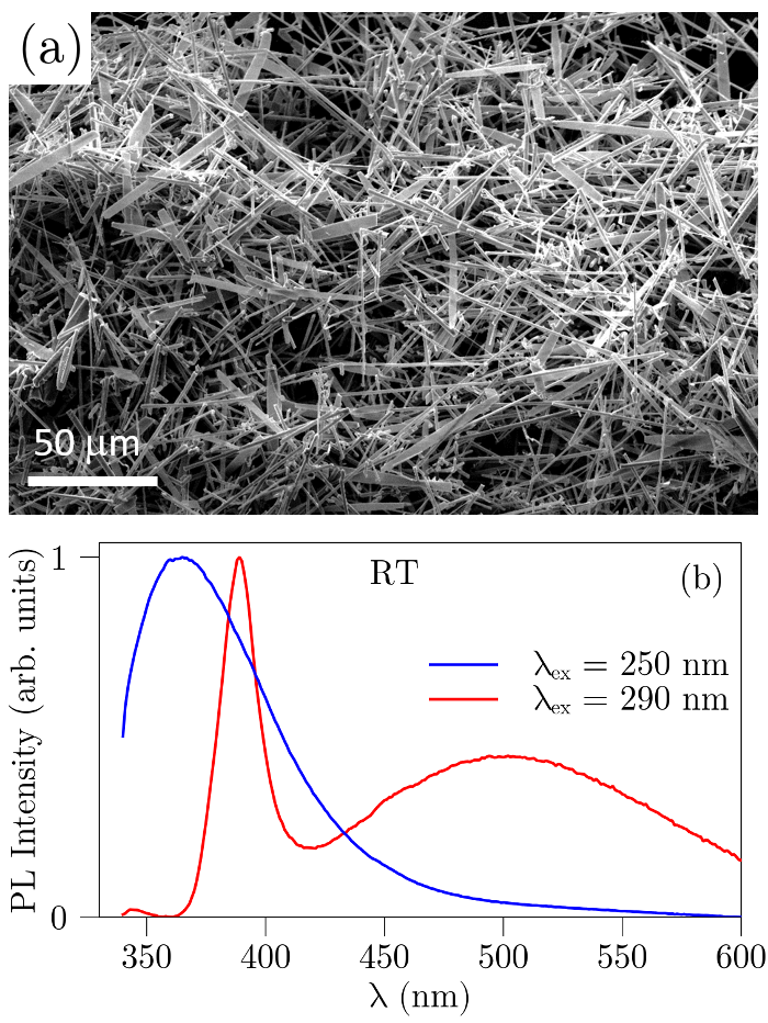
Herein, \ceZn2GeO4 micro-wires have been synthesized by a catalyst-free thermal evaporation method as described in the methodology section. The microstructural analysis of the microwires has been assessed by Raman spectroscopy and X-ray diffraction measurements and it has been already reported 18, 22. This procedure allows us to grow material of high crystalline quality. Figure 1(a) shows a representative SEM image of the network of \ceZn2GeO4 structures under study. Figure 1(b) shows the room temperature (RT) PL spectra obtained under different excitation wavelengths, covering the range from (), which is above the \ceZn2GeO4 bandgap ( at RT) up to (), below the bandgap. These PL spectra reveal at least two UV emission bands centered roughly at and , and another broad band peaked at . These bands are labelled as wide UV (W-UV), narrow UV (N-UV) and visible bands, respectively. For the sake of clarity, the PL spectra have been normalized to the N-UV emission band.
Most of the previous works on luminescence of \ceZn2GeO4 refer to room temperature experiments by exciting with energies under , and only observe the visible band related to DAP transitions, while the detection of the UV emission has been scarcely reported 18. Reported RT PL results also show that the maximum wavelength of the visible band varies from blue to green depending on the synthesis conditions, which is consistent with the interplay of several intrinsic defects in the luminescence mechanisms 23, 15. Oxygen vacancies in semiconducting oxides have been claimed as the responsible for their rather good electronic conductivity, due to their behaviour as donors centres, in spite of their wide bandgap. In some oxides, as in \ceGa2O3, some models proposed the formation of energy subbands within the bandgap providing delocalized electrons that contribute to the n-type electronic conductivity 24. The RT PL results of Figure 1 would support some partial conclusions about the light emission in \ceZn2GeO4. Firstly, the broad shape of the W-UV and visible bands suggests that they are originated from recombinations between donors related to oxygen vacancies and either the valence band or acceptors levels, respectively. Secondly, Figure 1(b) also shows that the emission bands strongly depend on the excitation wavelength. By exciting above the bandgap energy, only the W-UV band is produced while both the N-UV and the visible emission appear by exciting below the bandgap. This finding could explain the previous PL and CL results about getting UV emission under electron beam irradiation since CL provokes a higher excess carrier density that may recombine through all the available channels 18. Lastly, the occurrence of the N-UV band suggests that another recombination donor center of a more localized nature than the oxygen vacancies is also playing a role. Liu et al. have carried out electron paramagnetic resonance (EPR) measurements in \ceZn2GeO4 and proposed that, in addition to vacancies, Zn interstitial defects could also be involved as donor centers in the DAP processes 15.
To further investigate the intriguing nature of the UV emission bands, low temperature PL and PL excitation (PLE) measurements have been performed. Figure 2(a) displays a series of PL spectra at recorded under different excitation wavelengths. The broad W-UV band () is detected when exciting from , whereas the narrow N-UV band () is observed for all the excitation wavelengths. No visible emission is detected at low temperature. In order to clarify the excitation conditions for the W-UV and N-UV bands, PL excitation (PLE) spectra have been recorded and shown in Figure 2(b). We can observe that the W-UV band is only excited by energies above the bandgap (blue line), while the N-UV can also be excited with lower photon energies (red line). In addition, the N-UV is actually split into two components ( and ), clearly resolved when excitation is below the bandgap [see Figure 2(a)].
Therefore, from the above RT and PL results, we can conclude that different donor levels may be involved in the origin of the luminescence in \ceZn2GeO4, offering alternative pathways for radiative transitions to either acceptor levels (leading to the visible emission) or to the valence band (UV emissions). Thus, besides the oxygen vacancies acting as donor centres, other native defects of composite nature would bring about the N-UV band.
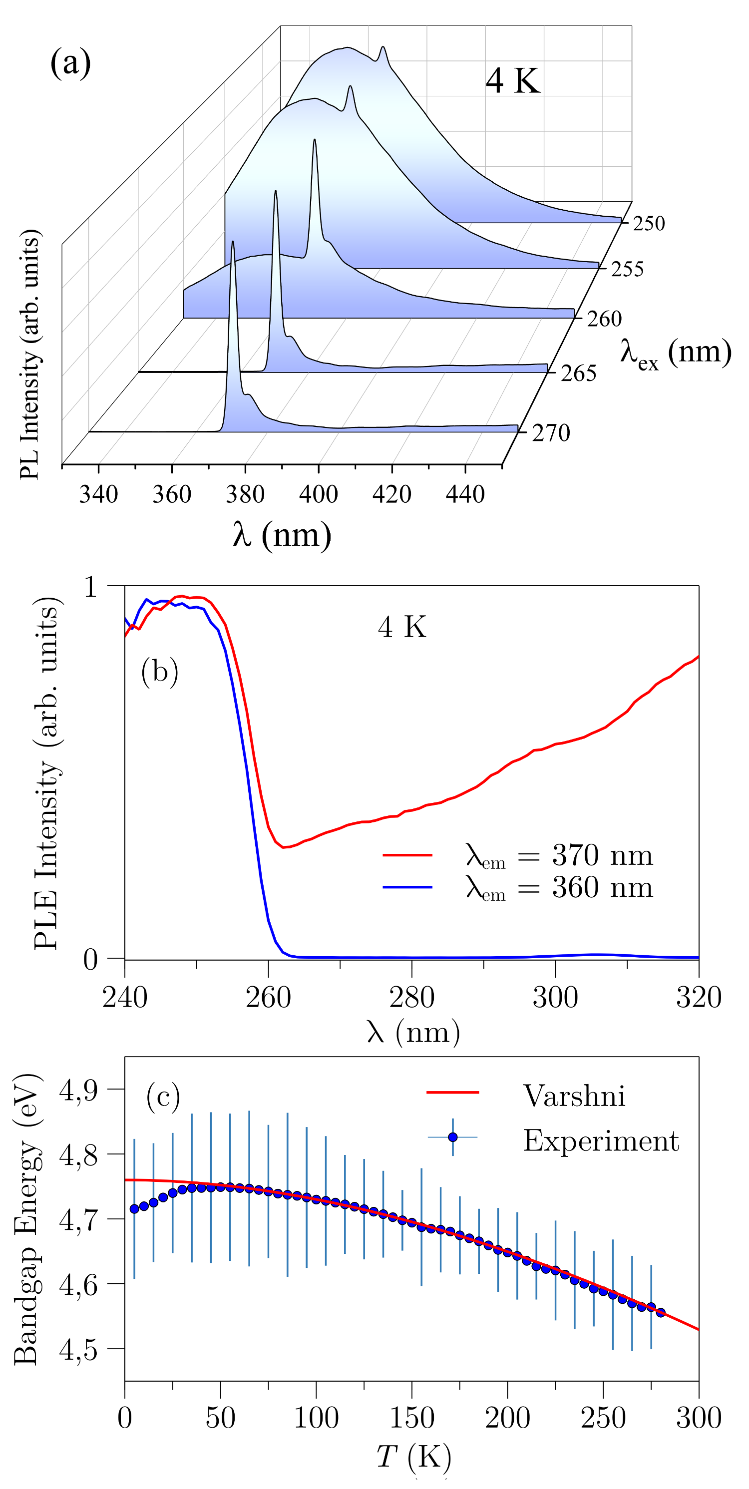
PLE measurements indirectly provide an estimated value of the optical bandgap in a semiconductor by extrapolating the sharp decay at the shortest wavelengths to a linear function 25. We have recorded PLE spectra from to RT, from which experimental values of are obtained and displayed in Figure 2(c). Data were fitted by the semi-empirical relationship postulated by the Varshni equation26
| (1) |
The temperature dependence of the bandgap is due to the effects of the thermal expansion of the lattice and the electron-phonon interaction. Usually, the balance between these effects produces a redshift of as temperature increases. The fitting of our data to Equation 1 yields , and , although an anomalous behaviour is observed in the low temperature regime, from . This anomaly has been reported in some semiconductors, such as \ceCuInS2, where it has been explained by the reduction of -levels in the upper valence band due to thermal expansion and the competition with the electron-phonon interaction 27.
The monitoring of the two components of the N-UV band resolved in Figure 2(a) as a function of the temperature has also been carried out. Figures 3(a) and 3(b) show a complete series of PL spectra under , from to RT. The selected allows us to study the nature and origin of the two components of the N-UV band as a function of temperature, without major contributions of the W-UV band. For the sake of clarity, PL curves have been separated into two plots, corresponding to low () and high () temperature range.
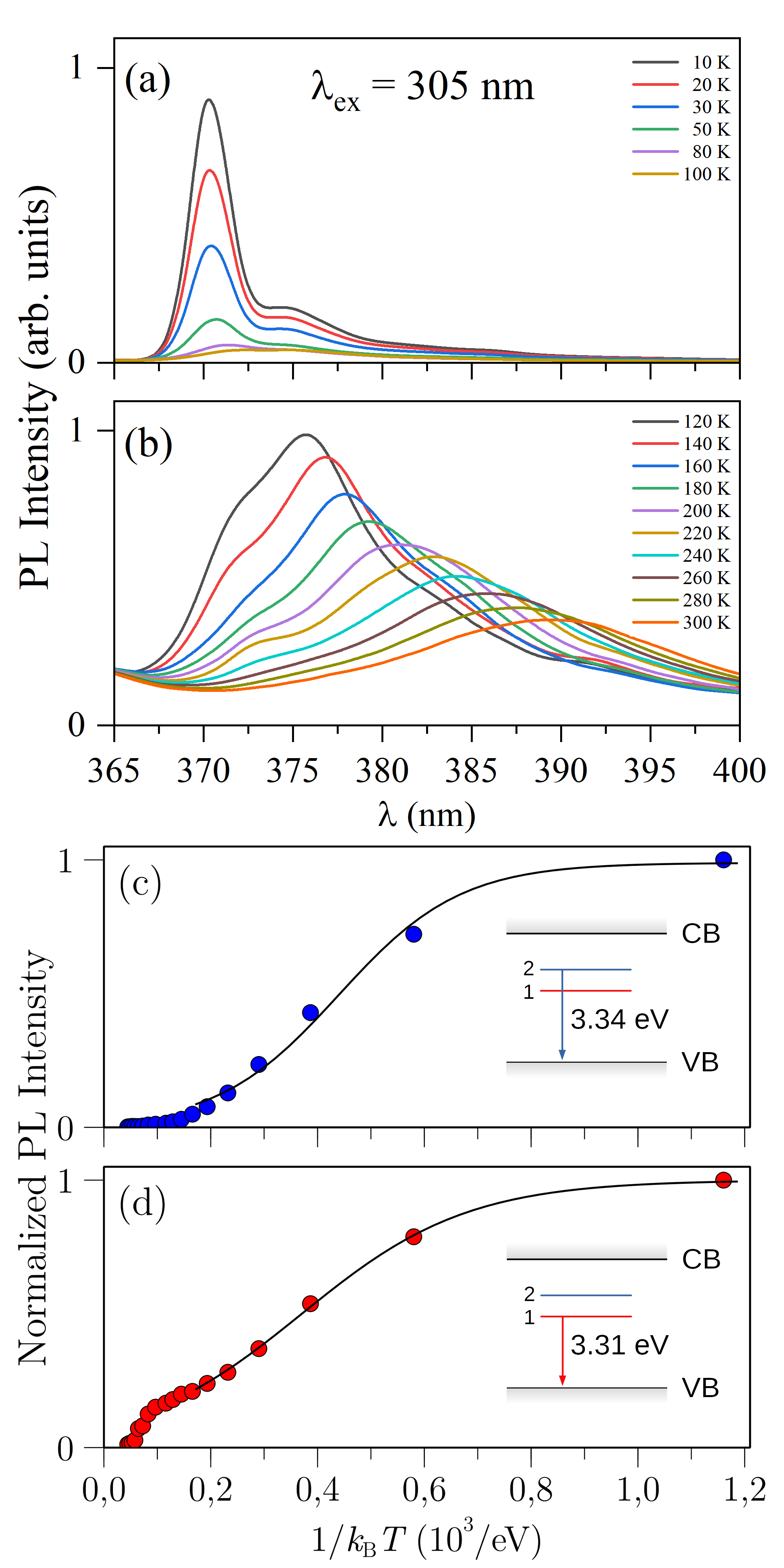
The analysis of the PL spectra as a function of the temperature gives rise to distinguish two temperature ranges. In the low temperature regime, from [see Figure 3(a)], there is a marked drop of the intensity of the band (N-UV2) relative to one (N-UV1). On the other hand, in the to RT range [Figure 3(b)], both components broaden in shape and experience a shift to lower energies. This different behaviour with temperature of the and bands leads us to consider that they could be originated from emission centers whose levels are close in energy. In some works, Zn defects have been proposed to be involved in luminescence processes in \ceZnO and \ceZn2GeO4 28, 15. Our results are consistent with the hypothesis that the N-UV emission originates from Zn related levels as well. The two components resolved in the N-UV band may be due to the two possible positions of the Zn in the \ceZn2GeO4 crystalline lattice, which would modify the local environment of the defect. In particular, there are two types of six-member rings in the \ceZn2GeO4 lattice that could host Zn at their centers. But in any case, both possible positions should be very similar since the energies of both centers are also similar, as we will show below from DFT calculations.
Therefore, the temperature-dependent PL data ground the following luminescence mechanisms for the UV bands. Excitation above the bandgap would populate the VO and Zn related levels that will be further recombined with holes of the valence band leading to the UV luminescence, as it is observed in Figure 2. In addition, the selective excitation at energies below the bandgap favors the N-UV emission at low temperature, suggesting a preferred recombination via Zn related levels. The composed nature of the N-UV band would then be explained by the two possible local environment of Zn defects. In the next subsections, we will show that these experimental findings are consistent with the first principle calculations results of defective \ceZn2GeO4. Finally, a kinetic model for the luminescence process is proposed, providing further support to the relation of these native defects with the radiative recombination channels observed in PL spectra.
2.2 First-principles calculations
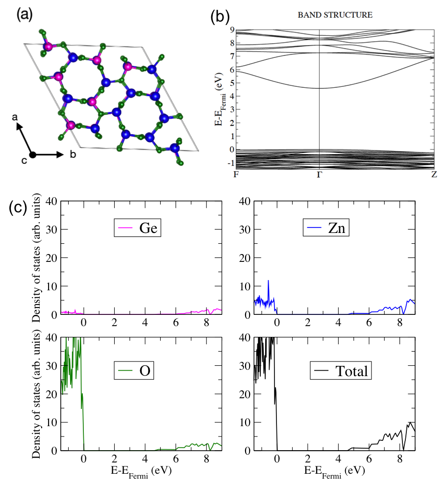
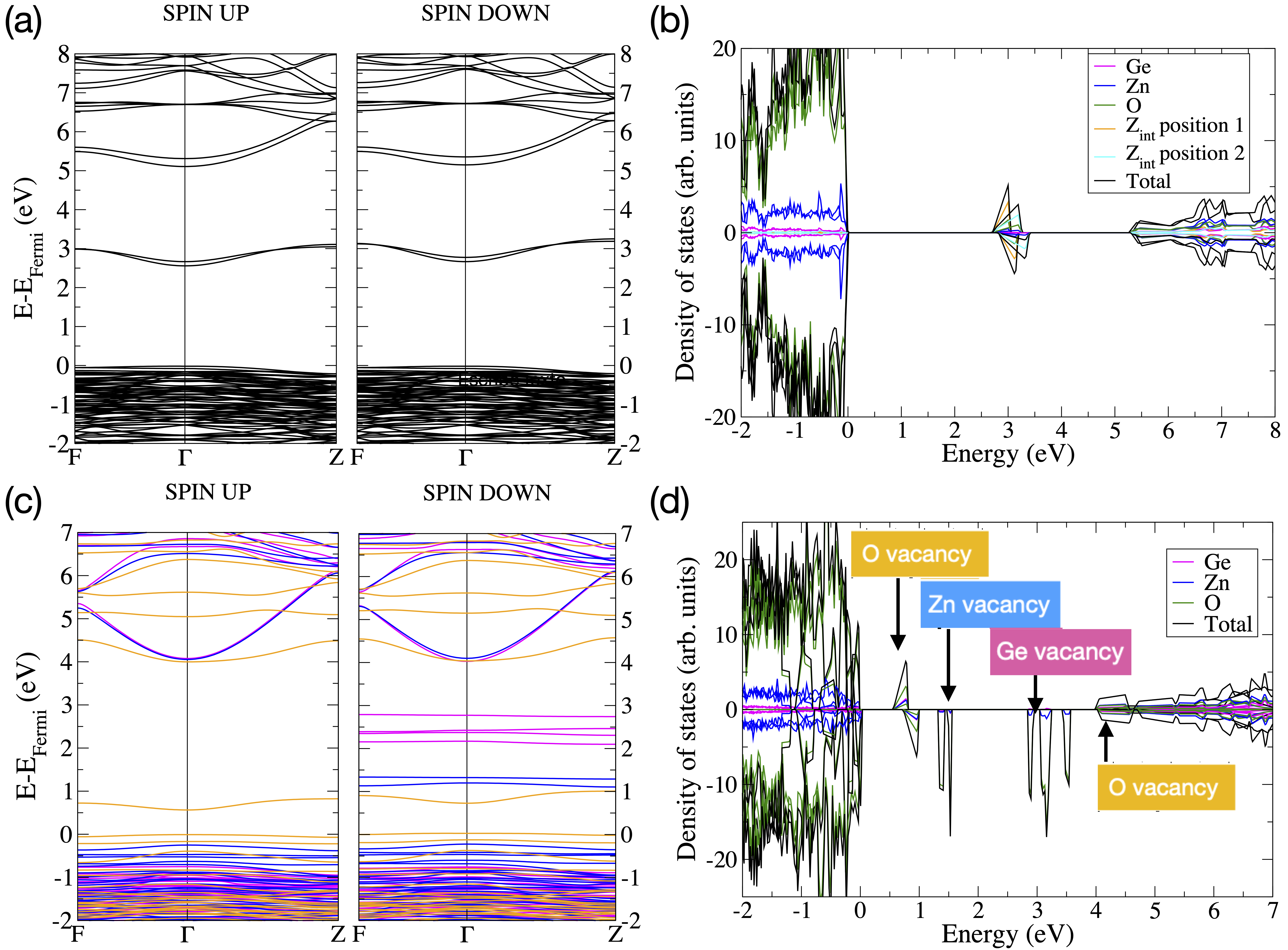
DFT calculations using the screened hybrid-exchange functional Heyd–Scuseria–Ernzerhof (HSE) 29 have been performed in order to analyze the effect of the native defects in the electronic structure of \ceZn2GeO4. The optimized unit cell can be seen in Figure 4(a), being the calculated lattice parameters ( and ) compatible with the rhombohedral phase of \ceZn2GeO4 (JCPDS11–0687). The density of states (DOS) and band structure for the stoichiometric \ceZn2GeO4 is shown in Figure 4(b) and (c). The conduction band is mainly composed of Zn-, Ge-, and O- orbitals, while the valence band is dominated by Zn- and O- orbitals. The calculated bandgap is , in excellent agreement with the experimental one at low temperature shown in Figure 1 ( at ).
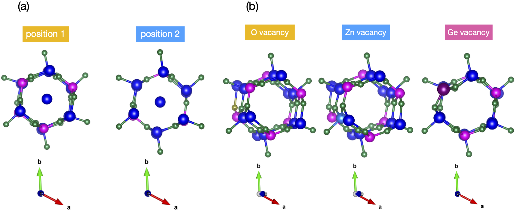
Let us now move on to the results of defective \ceZn2GeO4. DFT calculations of Zn states are presented in Figures 5 and 6. The Zn atom has been placed both at the center of the Zn-Ge ring (position 1) and Zn ring (position 2), as can be seen in Figure 5(a). The spin moment of the Zn atom (0.1 , is the Bohr magneton) leads to a DOS split into spin-up and spin-down states, and a dopant-induced state appears at the middle of the gap. The energies of the Zn states, which are located at around above from the valence band, are very similar in both structures, with an energy difference of around between them [see Figure 6 (a) and (b)] .
DFT results of O, Zn and Ge vacancy-related states are presented in Figures 5 and 6. The considered sites for the vacancy defects in \ceZn2GeO4 are shown in Figure 5(b). The two unpaired electrons generated by the oxygen vacancy lead to three different states in the gap. Two of them close to the valence band at (spin up) and (spin down), and another one very wide ( width) and close to the conduction band at . According to the Mulliken population analysis, electrons go to the oxygen vacancy site, electrons are placed at the Ge contiguous to the vacancy and the rest are distributed over the remaining of oxygen atoms in the unit cell. In the case of the Zn vacancy, two spin down states appear at and . These states are generated by the spin moment of two oxygen atoms. Finally, the three unpaired electrons created by the Ge vacancy generate a spin moment of 0.98 in three oxygen atoms, which correspond to three gap states at , and . The strong polarization that appears for both Ge and Zn vacancies have been previously reported in the literature 21. The formation energy of the vacancies is calculated by using the expression
| (2) |
where and are the total energies of the defective and non-defective structures, respectively. represents the total energy of O2 (X O), Zn2 (X Zn) and \ceGe2 (X Ge). The obtained formation energies for the O, Zn, and Ge vacancies are , , and , respectively. For the Zn defects, the formula used is
| (3) |
The resulting formation energies for Zn in position 1 and position 2 are and , respectively. The oxygen vacancy appears to be the most stable from the three considered ones, while the Zn defects are more favourable. These calculations are in agreement with the luminescence measurements in \ceZn2GeO4 shown above and provide some hints about the electronic levels involved in the PL emission bands. The broad nature of the oxygen vacancies related levels is confirmed from DFT and support the presence of broad emission bands associated with oxygen vacancies in the UV or in the visible. Regarding the UV emissions, excitation with photons of energy above the bandgap populates the conduction band enough so that relaxation via transitions from V and Zn levels to the valence band lead to W-UV and N-UV luminescence bands, respectively. On the other hand, when exciting with energies below the bandgap, only the Zn-related emission is observed [see Figure 2(b)] at low temperature.
2.3 Kinetics of the luminescent processes.
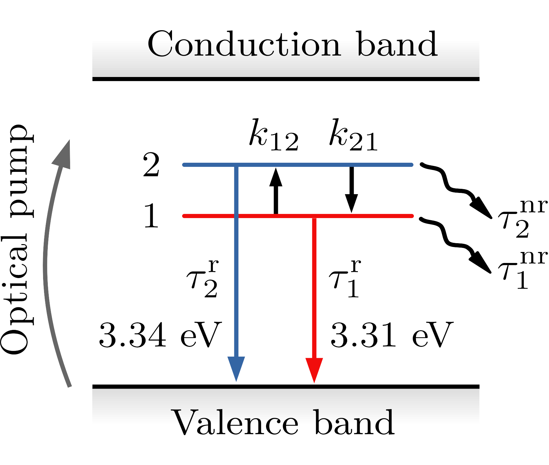
The energy band model and the relevant transitions to explain the observed low temperature dependence of the N-UV PL intensity are shown in Figure 7. After optical excitation with an energy below the bandgap, native defect levels become populated. Since the free-electron concentration in the conduction band is therefore negligible, the population of levels is only due to electrons generated by the optical pumping. Radiative and nonradiative channels deplete those levels. Let , and with be the energy, and the radiative and nonradiative decay time constants of such levels, respectively. To better understand the nature of the native defects, whether isolated or forming complexes, in this analysis we also consider transitions between the two levels and shown in Figure 7, with nonradiative rates and .
The concentration of occupied levels at a temperature and the total concentration of levels (occupied and empty) will be denoted as and , respectively. According to the model, we can write down the following kinetic equations
| (4) |
where the dependence of on time and temperature is understood. The decay time constants are given as and is the generation rate of level by the optical pump. Recently, Takahashi et al. found that the selective introduction of interstitial Zn defects in Zn2GeO4 yields a long-lasting PL emission 30. This finding agrees well with our observations and we thus take , namely in Equation (4).
Notice that in the absence of recombination mechanisms and interlevel transitions (i.e. and ), solution to Equation (4) would be simply given as , thus describing an exponential filling in time of the levels due to the optical pumping. It is most important to mention that we disregard electron capture on the empty levels in this model. The rate of electron capture is determined as , where 31. These processes would enter into the right-hand side of Equation (4) as a term of the form . At low temperature and photon excitation energy below the bandgap, both and are small () so we can neglect electron capture processes compared to the occupation of levels by optically generated electrons.
The interlevel rates and are not independent parameters since they must meet the principle of detailed balance , where is the energy of the electron level and is the Boltzmann constant. Thus, in the absence of decay channels, the eventual electron distribution would account for the Boltzmann equilibrium distribution (nondegenerate electrons). According to DFT calculations and PL measurements, the energy difference of the most relevant levels in zinc germanate is . Therefore, at low temperature, namely , we can assume that and retain hereafter.
With these assumptions in mind, Equation (4) in steady state leads to
| (5a) | ||||
| (5b) | ||||
Solving for and , we can obtain the following temperature dependence of the intensity of both PL bands as . Therefore, from Equations (5) we arrive at
| (6a) | ||||
| (6b) | ||||
According to Equation (6b), the intensity of the N-UV2 band () as a function of temperature can be cast in the form
| (7) |
where , and are temperature-independent parameters. Here is an activation energy for nonradiative recombination of electrons in the upper level (level in Figure 7). Figure 3(c) shows the PL intensity of the N-UV2 band () as a function of temperature and the corresponding non-linear fit to Equation (7) at low temperature (). The fitting parameters are , and . According to the relation of these parameters with the microscopic parameters of the model appearing in Equation (6b), we conclude that is vanishingly small compared to the generation rate of the upper level by the optical pumping since . In other words, nonradiative transitions from the upper level to the lower level are irrelevant. This result gives further support to the claim that both deep levels are related to different and spatially separated point defects.
We now turn our attention to the PL intensity of the N-UV1 band shown in Figure 3(d). From Equation (6a) with , the intensity of this band as a function of temperature is given as
| (8) |
where and are temperature-independent parameters. Here is an activation energy for nonradiative recombination of electrons in the lower level (level in Figure 7). Recall that this expression only holds in the low temperature regime. The non-linear fitting of the experimental data at low temperature () yields and . The fact that and are not very different from each other is consistent with the similar surroundings of both native defects, as suggested from our DFT calculations.
3 Conclusions
The UV luminescence bands of \ceZn2GeO4 have been in-depth studied as a function of temperature and excitation energy conditions. The relationship between native defects and electronic states has been explored by means of DFT to ascertain the origin of the observed luminescence bands. A broad and a narrow UV emissions have been recorded and associated to oxygen vacancies-related levels and zinc interstitials-related levels, respectively. The particular features of the N-UV emission have motivated the proposal of a kinetic model to explain its temperature dependence. The results show that this emission is quite stable upon temperature changes and is the only dominant emission when exciting below the energy bandgap in the low temperature regime, up to . The composite nature of this emission has been explained as originating from the two possible interstitial sites for Zn within the Zn-Ge or Zn rings in the lattice structure. The energies of the related levels calculated by DFT nicely match the position of the PL maxima observed. Besides, the temperature dependence in the low temperature regime of both components has been theoretically modeled, yielding activation energies of about .
3.1 Methodology
Experimental approach. The studied samples have been obtained by a thermal evaporation method that uses a compacted pellet of a mixture of Zn, Ge and graphite as source material. The precursors used have been pure ZnO, Ge and carbon powders with a weight ratio 2:1:2 18. Then, a thermal annealing at for 8 hours was conducted in an open tubular furnace not sealed under vacuum, leading to the growth of the \ceZn2GeO4 microstructures on the pellet. The microstructures were detached from the pellet and deposited on a silicon wafer for further characterization. The structural characterization has been carried out by grazing incidence X-ray diffraction (XRD) performed with a Philips X’Pert MRD Pro diffractometer. Raman measurements were conducted with the help of a Horiba Jobin Ybon LabRam Hr800 confocal microscope with excitation wavelength of . This optical microscope allows as well room temperature photoluminescence measurements. Finally, photoluminescence (PL) and PL excitation (PLE) spectra were acquired with an Edinburgh Instruments FLS1000 system at room temperature, exciting with a Xe lamp as excitation source.
Density Functional Theory calculations. All DFT calculations have been performed using the CRYSTAL program 32, in which the crystalline orbitals are expanded as a linear combination of atom-centered Gaussian orbitals, the basis set. The zinc, oxygen, and germanium ions are described using all-electron basis sets contracted as , and , respectively. Electronic exchange and correlation were approximated by using the Heyd–Scuseria–Ernzerhof (HSE) screened hybrid functional 29. In particular, the HSE06 functional with a mixing parameter of 0.25 has been used to describe the fundamental bandgap and electronic structure of ZnO, giving rise to underestimated bandgap values 33. A mixing factor of 0.33 has also been tested in ZnO, yielding better results 34. In order to check the suitability of this mixing factor for \ceZn2GeO4, we have performed a calculation using the HSE06 functional with a mixing factor of 0.33. The obtained bandgap with this mixing factor for stoichiometric \ceZn2GeO4 was of 5.2 eV, which is higher than our experimental value of 4.76 eV at 4K. However, the HSE06 with a mixing factor of 0.25 provides a bandgap of 4.62 eV, which is in excellent agreement with the experimental value and validates the considered model for \ceZn2GeO4. Integration over the reciprocal space was carried out using Monkhorst-Pack (MP) meshes of . The self-consistent field (SCF) algorithm was set to converge at the point at which the change in energy was less than Hartree per unit cell. The internal coordinates have been determined by minimization of the total energy within an iterative procedure based on the total energy gradient calculated with respect to the nuclear coordinates. Convergence was determined from the root-mean-square (rms) and the absolute value of the largest component of the forces. The thresholds for the maximum and the rms forces (the maximum and the rms atomic displacements) have been set to 0.00045 and 0.00030 (0.00180 and 0.0012) in atomic units. Geometry optimization was halted when all four conditions were satisfied simultaneously.
This work was supported by Ministerio de Ciencia, Innovación y Universidades (Grants MAT2016-75955 and RTI2018-09195-B-I00) and Deutsche Forschungsgemeinschaft (Grant CU 44/47-1).
References
- Tien et al. 2018 Tien, L.-C.; Yang, F.-M.; Huang, S.-C.; Fan, Z.-X.; Chen, R.-S. Single Zn2GeO4 nanowire high-performance broadband photodetector. J. Appl. Phys. 2018, 124, 174503
- Tak et al. 2019 Tak, B. R.; Gupta, V.; Kapoor, A. K.; Chu, Y.-H.; Singh, R. Wearable Gallium Oxide Solar-Blind Photodetectors on Muscovite Mica Having Ultrahigh Photoresponsivity and Detectivity with Added High-Temperature Functionalities. ACS Appl. Electron. Mater. 2019, 1, 2463 – 2470
- He et al. 2015 He, H.; Zhang, Y.; Pan, Q.; Wu, G.; Dong, G.; Qiu, J. Controllable synthesis of Zn2GeO4:Eu nanocrystals with multi-color emission for white light-emitting diodes. J. Mater. Chem. C 2015, 3, 5419 – 5429
- Sang et al. 2013 Sang, L.; Liao, M.; Sumiya, M. A Comprehensive Review of Semiconductor Ultraviolet Photodetectors: From Thin Film to One-Dimensional Nanostructures. Sensors 2013, 13, 10482–10518
- López et al. 2014 López, I.; Castaldini, A.; Cavallini, A.; Nogales, E.; Méndez, B.; Piqueras, J. -Ga2O3nanowires for an ultraviolet light selective frequency photodetector. J. Phys. D Appl. Phys. 2014, 47, 415101
- Zhao et al. 2015 Zhao, B.; Wang, F.; Chen, H.; Wang, Y.; Jiang, M.; Fang, X.; Zhao, D. Solar-Blind Avalanche Photodetector Based On Single ZnO–Ga2O3 Core–Shell Microwire. Nano Lett. 2015, 15, 3988 – 3993
- Su et al. 2014 Su, L.; Zhu, Y.; Yong, D.; Chen, M.; Ji, X.; Su, Y.; Gui, X.; Pan, B.; Xiang, R.; Tang, Z. Wide Range Bandgap Modulation Based on ZnO-based Alloys and Fabrication of Solar Blind UV Detectors with High Rejection Ratio. ACS Appl. Mater. Interfaces 2014, 6, 14152 – 14158
- Mizoguchi et al. 2011 Mizoguchi, H.; Kamiya, T.; Matsuishi, S.; Hosono, H. A germanate transparent conductive oxide. Nat. Commun. 2011, 2, 470
- Wang et al. 2013 Wang, J.; Yan, C.; Magdassi, S.; Lee, P. S. Zn2GeO4 Nanowires As Efficient Electron Injection Material for Electroluminescent Devices. ACS Appl. Mater. Interfaces 2013, 5, 6793 – 6796
- Zhou et al. 2016 Zhou, X.; Zhang, Q.; Gan, L.; Li, X.; Li, H.; Zhang, Y.; Golberg, D.; Zhai, T. High—Performance Solar-Blind Deep Ultraviolet Photodetector Based on Individual Single-Crystalline Zn2GeO4 Nanowire. Adv. Funct. Mater. 2016, 26, 704 – 712
- Yi et al. 2013 Yi, R.; Feng, J.; Lv, D.; Gordin, M. L.; Chen, S.; Choi, D.; Wang, D. Amorphous Zn2GeO4 nanoparticles as anodes with high reversible capacity and long cycling life for Li-ion batteries. Nano Energy 2013, 2, 498 – 504
- Maestre et al. 2004 Maestre, D.; Cremades, A.; Piqueras, J. Cathodoluminescence of defects in sintered tin oxide. J. Appl. Phys. 2004, 95, 3027 – 3030
- Stichtenoth et al. 2008 Stichtenoth, D.; Dürr, J.; Ronning, C.; Wischmeier, L.; Voss, T. Characterization of the donor-acceptor-pair transition in nitrogen-implanted zinc oxide. J. Appl. Phys. 2008, 103, 083513
- López et al. 2016 López, I.; Alonso-Orts, M.; Nogales, E.; Méndez, B.; Piqueras, J. Influence of Li doping on the morphology and luminescence of Ga2O3 microrods grown by a vapor-solid method. Semicond. Sci. Technol. 2016, 31, 115003
- Liu et al. 2007 Liu, Z.; Jing, X.; Wang, L. Luminescence of Native Defects in Zn2GeO4. J. Electrochem. Soc. 2007, 154, H500 – H506
- Pham et al. 2016 Pham, V.-H.; Kien, V. T.; Tam, P. D.; Huy, P. T. Luminescence of one dimensional ZnO, GeO2–Zn2GeO4 nanostructure through thermal evaporation of Zn and Ge powder mixture. Mat. Sci. Eng. B 2016, 209, 17 – 22
- Tsai et al. 2013 Tsai, M.-Y.; Huang, S.-H.; Perng, T.-P. Low temperature synthesis of Zn2GeO4 nanorods and their photoluminescence. J. Lumin. 2013, 136, 322 – 327
- Hidalgo et al. 2016 Hidalgo, P.; López, A.; Méndez, B.; Piqueras, J. Synthesis and optical properties of Zn2GeO4 microrods. Acta Mater. 2016, 104, 84 – 90
- Nogales et al. 2011 Nogales, E.; Hidalgo, P.; Lorenz, K.; Méndez, B.; Piqueras, J.; Alves, E. Cathodoluminescence of rare earth implanted Ga2O3and GeO2nanostructures. Nanotechnology 2011, 22, 285706
- Liu et al. 2013 Liu, L.; Zhao, X.; Sun, H.; Jia, C.; Fan, W. Theoretical Study of H2O Adsorption on Zn2GeO4 Surfaces: Effects of Surface State and Structure–Activity Relationships. ACS Appl. Mater. Interfaces 2013, 5, 6893 – 6901
- Xie et al. 2015 Xie, Z.-Y.; Lu, H.-L.; Zhang, Y.; Sun, Q.-Q.; Zhou, P.; Ding, S.-J.; Zhang, D. W. The electronic structures and optical properties of Zn2GeO4 with native defects. J. Alloys Compd. 2015, 619, 368 – 371
- Dolado et al. 2020 Dolado, J.; Renforth, K. L.; Nunn, J. E.; Hindsmarsh, S. A.; Hidalgo, P.; Sánchez, A. M.; Méndez, B. Zn2GeO4/SnO2 Nanowire Heterostructures Driven by Plateau–Rayleigh Instability. Cryst. Growth Des. 2020, 20, 506 – 513
- Tang et al. 2016 Tang, H.; Zhu, X.; He, H. Vapor phase growth and photoluminescence of oriented-attachment Zn2GeO4 nanorods array. J. Cryst. Growth 2016, 451, 170 – 173
- Binet and Gourier 1998 Binet, L.; Gourier, D. Origin of the blue luminescence of -Ga2O3. J. Phys. Chem. Solids 1998, 59, 1241 – 1249
- Masai et al. 2013 Masai, H.; Yamada, Y.; Suzuki, Y.; Teramura, K.; Kanemitsu, Y.; Yoko, T. Narrow energy gap between triplet and singlet excited states of Sn2+ in borate glass. Sci. Rep. 2013, 3, 3541
- Varshni 1967 Varshni, Y. P. Temperature dependence of the energy gap in semiconductors. Physica 1967, 34, 149 – 154
- Hsu and Lin 1988 Hsu, T. M.; Lin, J. H. Anomalous temperature-dependent band gaps in studied by surface-barrier electroreflectance. Phys. Rev. B 1988, 37, 4106 – 4110
- Wagner et al. 2011 Wagner, M. R. et al. Bound excitons in ZnO: Structural defect complexes versus shallow impurity centers. Phys. Rev. B 2011, 84, 035313
- Heyd et al. 2003 Heyd, J.; Scuseria, G. E.; Ernzerhof, M. Hybrid functionals based on a screened Coulomb potential. J. Chem. Phys. 2003, 118, 8207 – 8215
- Takahashi et al. 2010 Takahashi, Y.; Ando, M.; Iwasaki, K.; Masai, H.; Fujiwara, T. Defect activation in willemite-type Zn2GeO4 by nanocrystallization. Appl. Phys. Lett. 2010, 97, 071906
- Colbow and Nyberg 1968 Colbow, K.; Nyberg, D. Recombination kinetics in cadmium sulfide. J. Phys. Chem. Solids 1968, 29, 509 – 519
- Dovesi et al. 2018 Dovesi, R.; Erba, A.; Orlando, R.; Zicovich-Wilson, C. M.; Civalleri, B.; Maschio, L.; Rerat, M.; Casassa, S.; Baima, J.; Salustro, S.; Kirtman, B. Quantum‐mechanical condensed matter simulations with CRYSTAL. Wires Comput. Mol. Sci. 2018, 8, e1360
- Wròbel et al. 2009 Wròbel, J.; Kurzydlowsi, K. J.; Hummer, K.; Kresse, G.; Piechota, J. Calculations of ZnO properties using the Heyd-Scuseria-Ernzerhof screened hybrid density functional. Phys. Rev. B 2009, 80, 155124
- Clark et al. 2010 Clark, S. J.; Robertson, J.; Lany, S.; Zunger, A. Intrinsic defects in ZnO calculated by screened exchange and hybrid density functionals. Phys. Rev. B 2010, 81, 115311