Optical conductivity and resistivity in a four-band model for ZrTe5 from ab-initio calculations
Abstract
ZrTe5 is considered a potential candidate for either a Dirac semimetal or a topological insulator in close proximity to a topological phase transition. Recent optical conductivity results motivated a two-band model with a conical dispersion in 2D, in contrast to density functional theory calculations. Here, we reconcile the two by deriving a four-band model for ZrTe5 using theory, and fitting its parameters to the ab-initio band structure. The optical conductivity with an adjusted electronic structure matches the key features of experimental data. The chemical potential varies strongly with temperature, to the point that it may cross the gap entirely between zero and room temperature. The temperature-dependent resistivity displays a broad peak, and confirms theoretically the conclusions of recent experiments attributing the origin of the resistivity peak to the large shift of the chemical potential with temperature.
I Introduction
ZrTe5 is currently attracting renewed attention from two different perspectives. The first was sparked when density functional theory (DFT) calculations claimed this material to be a strong topological insulator (STI) close to a topological phase transition towards a weak topological insulator (WTI) Weng et al. (2014). Further computational work argued that this transition could be achieved via volume expansion Fan et al. (2017); Monserrat and Narayan (2019). Experimentally, the situation is debated: a combination of scanning-tunnelling microscopy (STM), angle-resolved photoemission spectroscopy (ARPES), and ab-initio calculations determined a gapped bulk electronic structure and topological states at the step edges, and ZrTe5 was concluded to be WTI Li et al. (2016a); Wu et al. (2016); Moreschini et al. (2016); Xiong et al. (2017). Yet, this result was in contradiction with other work performed at the same time using the same experimental probes, which determined that it is an STI Manzoni et al. (2016).
In the second perspective, ZrTe5 is claimed to be a Dirac semimetal following the measurement of the chiral magnetic effect Li et al. (2016b), as well as linear optical conductivity at low frequency Chen et al. (2015a). Reports of Shubnikov–de Haas (SdH) oscillations with a non-trivial Berry phase strengthened this claim, and unveiled a strongly anisotropic electronic structure Yuan et al. (2016); Zheng et al. (2016); Qiu et al. (2016). The Landau level spectrum showed Dirac semimetal features, in addition to band inversion Chen et al. (2015b, 2017); Jiang et al. (2017). Finally, a giant planar Hall resistivity, vanishing with the thickness of the sample, was observed and also interpreted as a signature of a Dirac semimetal Li et al. (2018).
ZrTe5 has been studied since the 1980s, before the rising interest in topological properties, owing to a prominent peak in the temperature dependent resistivity, in relation to a large thermoelectric power Jones et al. (1982); Skelton et al. (1982); Tritt et al. (1999). ARPES measurements linked this peak to a crossover from -type to -type carriers when decreasing temperature McIlroy et al. (2004); Manzoni et al. (2015); Xiong et al. (2017); Zhang et al. (2017), which concurred with a sign change of the Hall number Li et al. (2018); Martino et al. (2019). The temperature of the resistivity maximum varied with sample thickness and doping Lu et al. (2017); Tang et al. (2018); Li et al. (2019). Recently, this resistivity peak was also related to the potential topological properties of ZrTe5 and interpreted as a signature for a transition upon cooling Nair et al. (2018) from a WTI to an STI state Xu et al. (2018) or the reverse Tian et al. (2019), as well as a signature of Dirac polarons Fu et al. (2020).
Differences between synthesis methods were shown to strongly influence the electronic properties, in particular for samples with -doping in the case of chemical vapor transport growth, claimed to be responsible for the resistivity peak, as supported by ab-initio calculations Shahi et al. (2018).
Recently, a tentative minimal model for ZrTe5 was put forward, based on optical conductivity measurements Martino et al. (2019); Wang and Li (2020); Rukelj et al. (2020). In contrast to a 3D Dirac semimetal model, it features a linear dispersion in two directions and parabolic dispersion in the orthogonal direction. This important step attempts to describe theoretically experimental findings which have challenged theory until now. However, it falls short of completely uniting the field by also linking these experiments to the DFT results which initially sparked the interest for this material. In particular, this minimal model has a parabolic dispersion along the stacking direction, unlike the band structure calculated using DFT which features a double well structure. Additionally, it neglects the spin degree of freedom by considering only two bands, while DFT yields four bands, which are spin degenerate.
Here, we bridge this gap by starting from ab-initio calculations and fitting an alternative minimal model, obtained from theory, to the calculated bands. We adjust the electronic structure by modifying one parameter of the model, in particular changing the energy gap, known to be given inaccurately by DFT, to its experimental value. We calculate the optical conductivity, the temperature-dependent chemical potential and the resistivity, and find a frequency dependence of the optical conductivity matching experiments, without a parabolic dispersion along the stacking direction. The chemical potential strongly shifts at low temperature and thereby leads to a peak in the temperature-dependent resistivity, in agreement with ARPES and transport results.
II Ab-initio calculations
| a) | 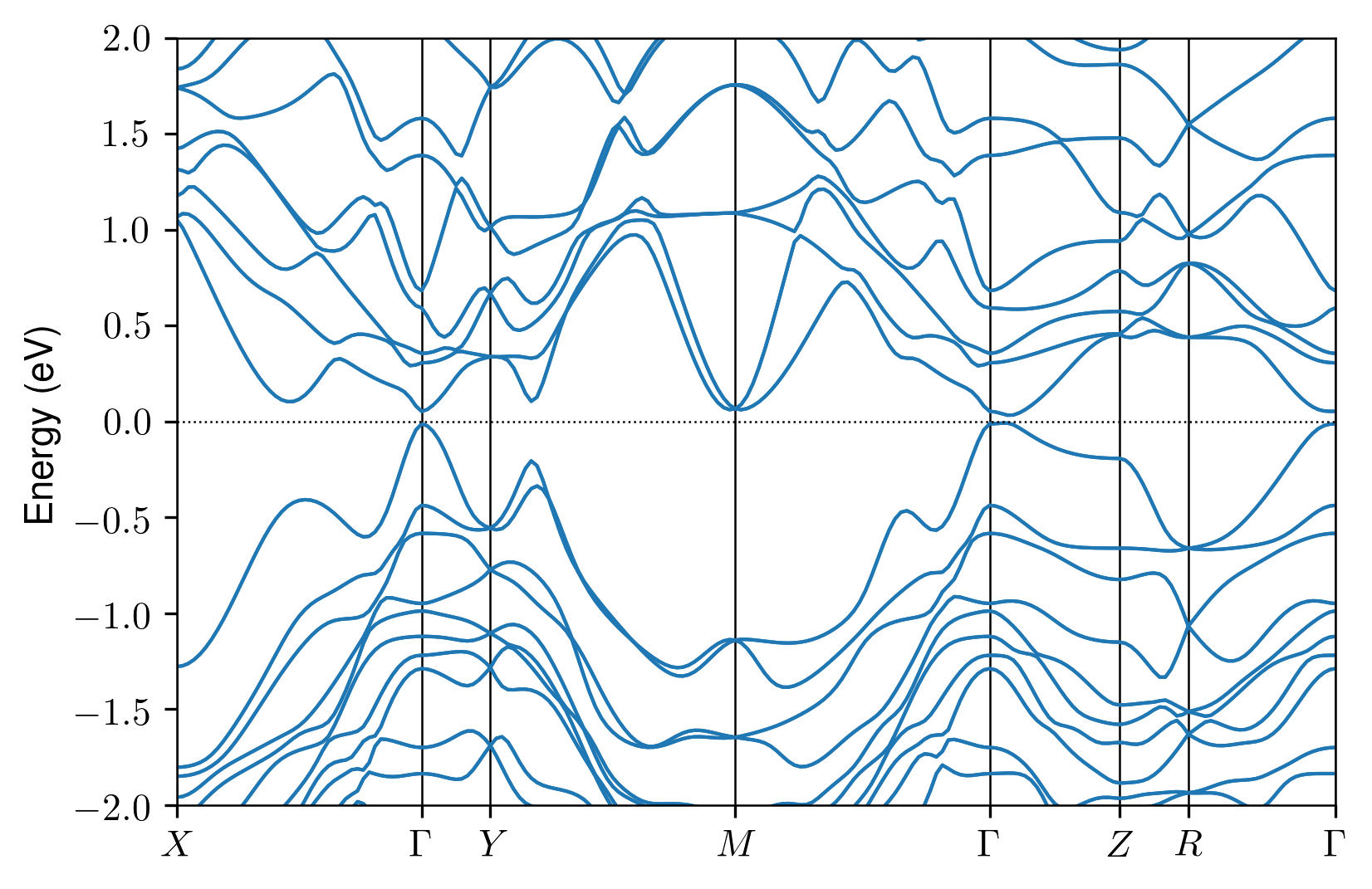 |
|---|---|
| b) | 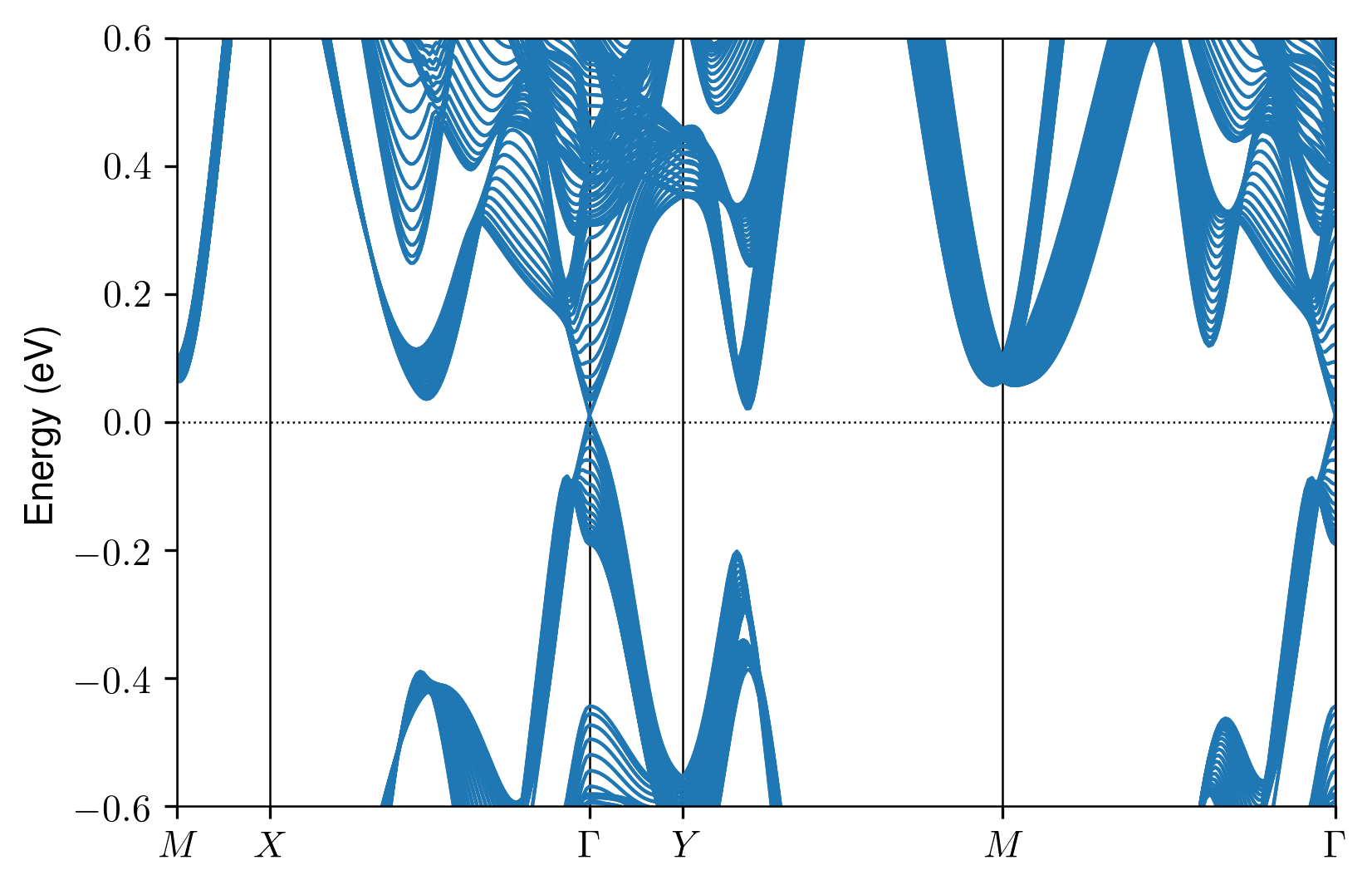 |
We calculated the electronic structure using fully relativistic projector augmented-wave pseudopotentials and a plane-wave basis set as implemented in Quantum Espresso, and the all-electron full-potential linearized augmented plane-wave code Elk. We employed the generalised gradient approximation in the shape of the Perdew, Burke, and Ernzerhof functional Perdew et al. (1996), and included spin-orbit coupling. We used the experimentally-measured crystal structure with Å, Å and Å Fjellvåg and Kjekshus (1986). ZrTe5 is composed of tubes of Te atoms surrounding chains of Zr atoms. These tubes are linked together to form two-dimensional layers in the - plane, which are coupled by van der Waals interactions along . The calculations were performed with k-points in the primitive unit cell and a plane-wave energy cutoff of 70 Ry in Quantum Espresso Giannozzi et al. (2009), and a predefined high-quality set of parameters in Elk Elk (2004). All the parameters were tested for convergence. The band structures calculated by the two methods are in close agreement. We constructed a tight-binding model by projecting the electronic structure obtained with Quantum Espresso on maximally localised Wannier orbitals using Wannier90 Pizzi et al. (2019). The Zr orbitals and Te orbitals were included in the model. We then used this tight-binding model to calculate topological indices and slab band structures using Wannier Tools Wu et al. (2018).
The band structure obtained in Elk is represented in Fig. 1a. It features states close to the Fermi level at , which get closer together on a short segment close to in the direction before growing further apart. At , the band gap is 65 meV, while the minimum gap along is 41 meV. Even though Zr atoms have a partially filled -shell and on-site correlations were not included in the calculations, the electronic structure exhibits a gap. This indicates that the physics of ZrTe5 close to the Fermi level is not dictated by strong correlations. We calculated the 3D topological invariants to be , and the band structure calculation for a slab perpendicular to the crystallographic direction (Fig. 1b) gives surface states close to , as expected for these invariants. These results are consistent with recent ab-initio studies of ZrTe5 Weng et al. (2014); Manzoni et al. (2016); Fan et al. (2017).
III Minimal model
We want to address the nature of the electronic structure of ZrTe5 close to the Fermi level. DFT is instrumental in doing so, since it fits ARPES results very well, except for the magnitude of the gap Wu et al. (2016); Martino et al. (2019). Many-body calculations, such as the GW approximation Hedin and Lundqvist (1969), and hybrid exchange-correlation functionals, such as B3LYP Becke (1993) and HSE Heyd et al. (2003), significantly improve the calculated gaps, at a high computational cost. Here, we take a different, more flexible route, by mapping our DFT results on a simple model which is easier to use in calculations of experimental responses, and which can be adapted to compensate for the shortcoming of DFT calculations that is the value of the gap.
The double point group associated to the space group at is . We calculated that the bands just below (respectively just above) the Fermi level are associated with the irreducible representations (respectively ) of this double point group. The character table for these two irreducible representations is:
| 2 | -2 | 0 | 0 | 0 | 2 | -2 | 0 | 0 | 0 | |
| 2 | -2 | 0 | 0 | 0 | -2 | 2 | 0 | 0 | 0 |
We constructed a model Hamiltonian for the four bands closest to the Fermi level using theory, which yields Hamiltonians in powers of reciprocal coordinates constrained by symmetry. Since we are considering two irreducible representations, each of which has spin degeneracy, our Hamiltonian is four-dimensional. We chose , and as a basis for . The matrices for these operations in the basis of the spinor are:
| (1) |
| (2) |
| (3) |
where is the inversion operator in real space. To second order in , , and , we obtain Gresch (2018):
where we used the functions:
| (4) | |||
| (5) |
, and are given in inverse lattice units. In the following, we refer to this as the parabolic model.
We determined the parameters of the model by fits to the band structure calculated with Elk close to along the three axes of the Brillouin zone. The fitted parameters are eV, eV, eV, eV, eV, eV, eV, eV, eV, eV, and eV.
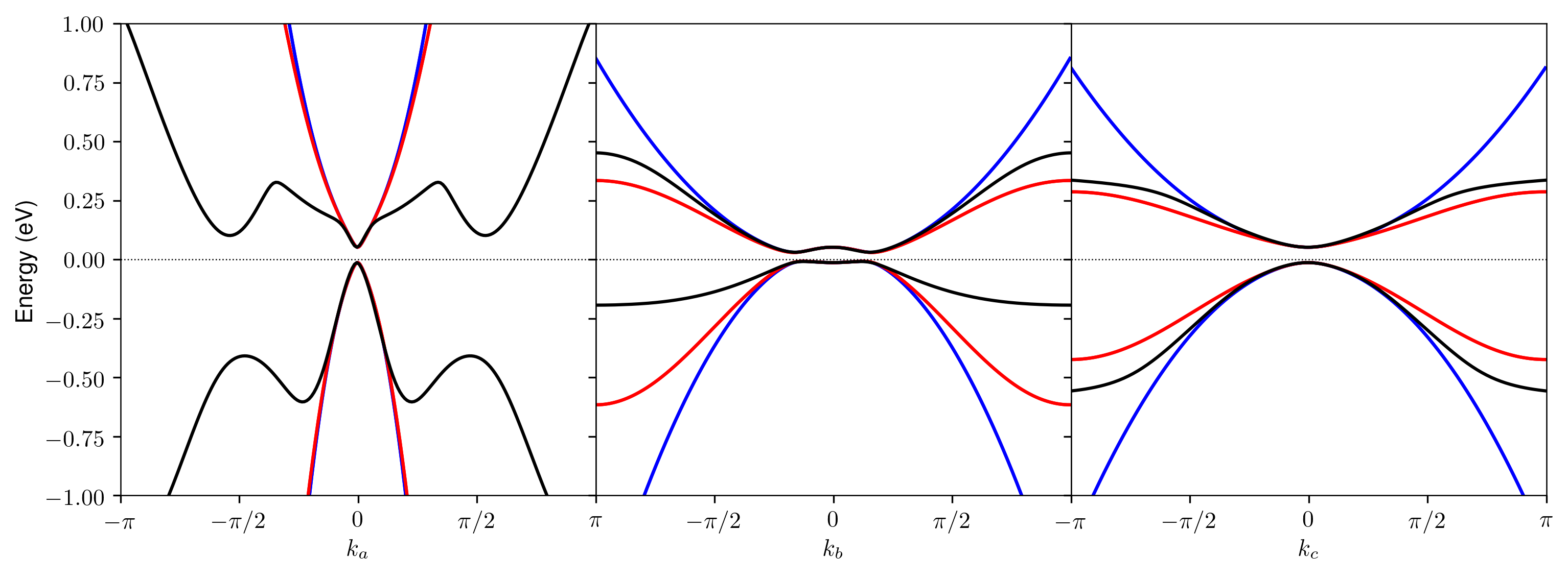
The quality of the fitted model is demonstrated in Fig. 2. Along and , the effective mass is large and the fit holds for a larger portion of the Brillouin zone. However along the effective mass is much smaller, the DFT band structure has more features and the fit only holds for . Importantly, the model describes well the double-peak and double-well structure in the dispersion along . The effective dispersion is very flat along this axis. This could be related to optical conductivity results which point to a parabolic dispersion along Martino et al. (2019).
We adapted the model to the case of a lattice by using the standard substitutions and . The result is shown in Fig. 2, and compares well to the DFT band structure close to . The widths of the lattice and DFT bands are close to each other along and , while the DFT bands have a smaller width along . The topological invariants of the lattice model are , which are different from those of the DFT bands. This is unsurprising since the band inversion in ZrTe5 happens away from Manzoni et al. (2016), whereas the model parameters were obtained by fitting close to ; it is a common issue with theory Nechaev and Krasovskii (2016); Choi et al. (2020).
IV Optical conductivity
Now that we have justified the theory model in comparison to ab-initio calculations, we test its validity with respect to experimental data. We calculated the longitudinal optical conductivity along as Tkachov (2016):
| (6) |
where is the frequency, the temperature, the crystal volume, and band indices, k the crystal momentum, denotes eigenvalues of , is the Fermi-Dirac distribution, and is a lifetime broadening from residual scattering.
The value of can be related to the mean free path, which can be estimated as . The Fermi velocity along just above the Fermi level and off the point for between 3 and 33 meV is of the order of m/s. We choose meV which yields a mean free path of 300 nm, in accordance with the experimental values m/s and 583 nm Martino et al. (2019); Yang et al. (2019).
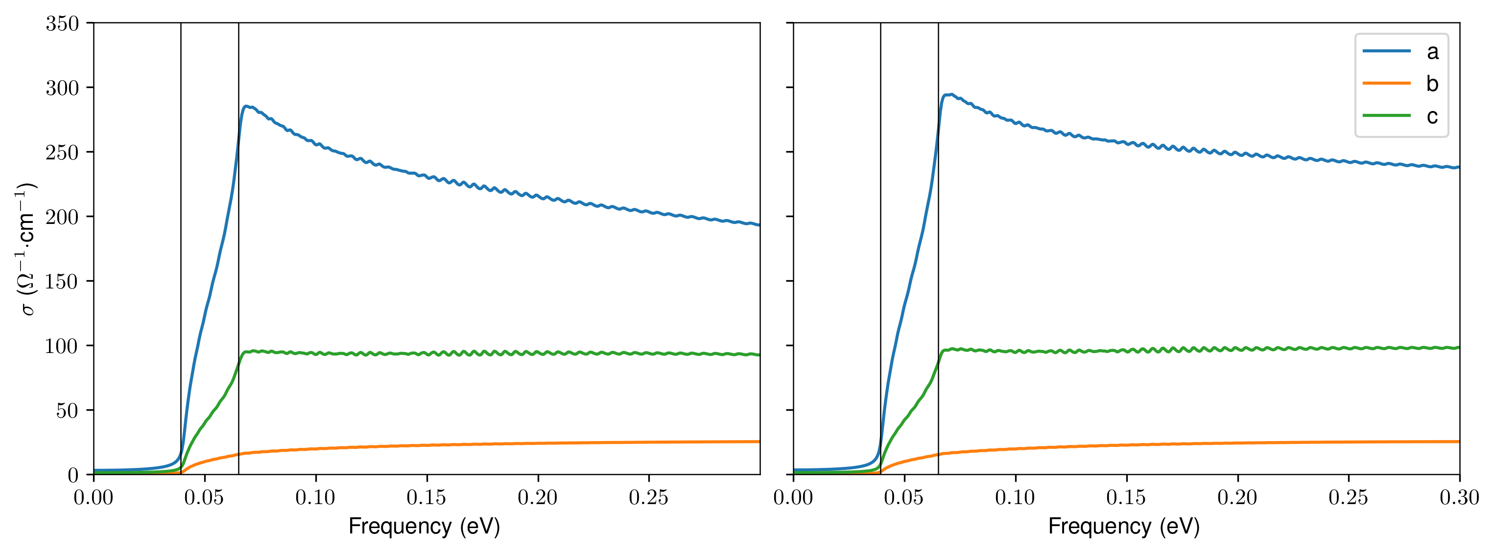
The calculated optical conductivity along , and for the parabolic model as a function of frequency at K is plotted in Fig. 3. is vanishingly small at low frequencies, and rises sharply around 40 meV, to reach around 300 cm-1, which is very close to the value measured experimentally Martino et al. (2019). There is a shoulder in this rise, which we attribute to the double well electronic structure along . Also indicated are the values of the minimal gap along and of the gap at , which coincide with the initial rise and levelling regime, respectively. At higher frequencies, the optical conductivity monotonically decreases. The optical conductivities along and follow a very similar trend. Their overall magnitudes differ by a factor three and both stay almost constant above the gap. The difference in magnitude between the optical conductivities along and is in line with the different flatnesses of the electronic bands along and , and is close to the difference measured experimentally Martino et al. (2019), which is also close to a factor of 3. The optical conductivity along is much smaller on account of the sizably reduced dispersion along , and globally follows the evolution of the one along , except that its rise at low frequency is smoother.
The optical conductivities for the parabolic and lattice models, plotted in Fig. 3, are very similar to the results for the parabolic model as expected. The optical conductivity along has not been measured yet and therefore constitutes a prediction which could be used to confirm the validity of the model presented here.
The most important point in the evolution of the optical conductivity along and is that the high-frequency behaviour for meV extrapolates to a finite value at zero frequency. This is a key signature that, according to Ref. Martino et al. (2019), excludes the possibility of a Dirac dispersion close to . Indeed, a Dirac dispersion would give a linear optical conductivity close to zero frequency. The experimental behaviour is successfully replicated by a two-band model with a parabolic dispersion along , which yields an optical conductivity going as the square root of the frequency Martino et al. (2019). In the same work, it is argued that this signature is also incompatible with a gapped Dirac model, which would give a linear optical conductivity with a shift in energy. At first sight, this is in contradiction with our results: the model we consider is a Dirac model with a k-dependent mass term. However the type of gapped Dirac model discussed in Ref. Martino et al. (2019) is very specific: it is a model where the dispersion is strictly linear above the gap, and features a discontinuous derivative at . Our result therefore provides an alternative scenario in which the optical conductivities from above 60 meV extrapolate to finite values at zero frequency. Moreover this scenario is in line with the proximity to a 3D Dirac state.
A second important point with respect to experiments is the presence of an inflection point in the sharp rise of the optical conductivity at low frequency. This matches the experimental data for on one of the two samples in Ref. Martino et al. (2019), modeled using a parabolic dispersion along .
Finally, one point does not fit experiments: after the sharp rise, the slope of the optical conductivity along turns negative, unlike the experimental data where it keeps on rising but much slower Martino et al. (2019). Our model is however entirely based on ab-initio calculations, which are known not to give correct estimates of band gaps. In the next section, we use the flexibility of our model to modify the electronic structure by adjusting , which in particular changes the gap to the experimental value.
V Adjusting the electronic structure
Experimental measurements yielded a large range of band gaps: ARPES results alone range between 0 and 100 meV Xiong et al. (2017). Since we are considering a simple model, we can adjust it to fit various experimental gaps. The gap at in our model is . We know that ARPES data fit DFT calculations away from Wu et al. (2016); Martino et al. (2019), so we keep the other parameters fixed, and only modify to compare it specifically with the optical conductivity measured along in Martino et al. (2019). The sample used for these measurements had a band gap of 6 meV.
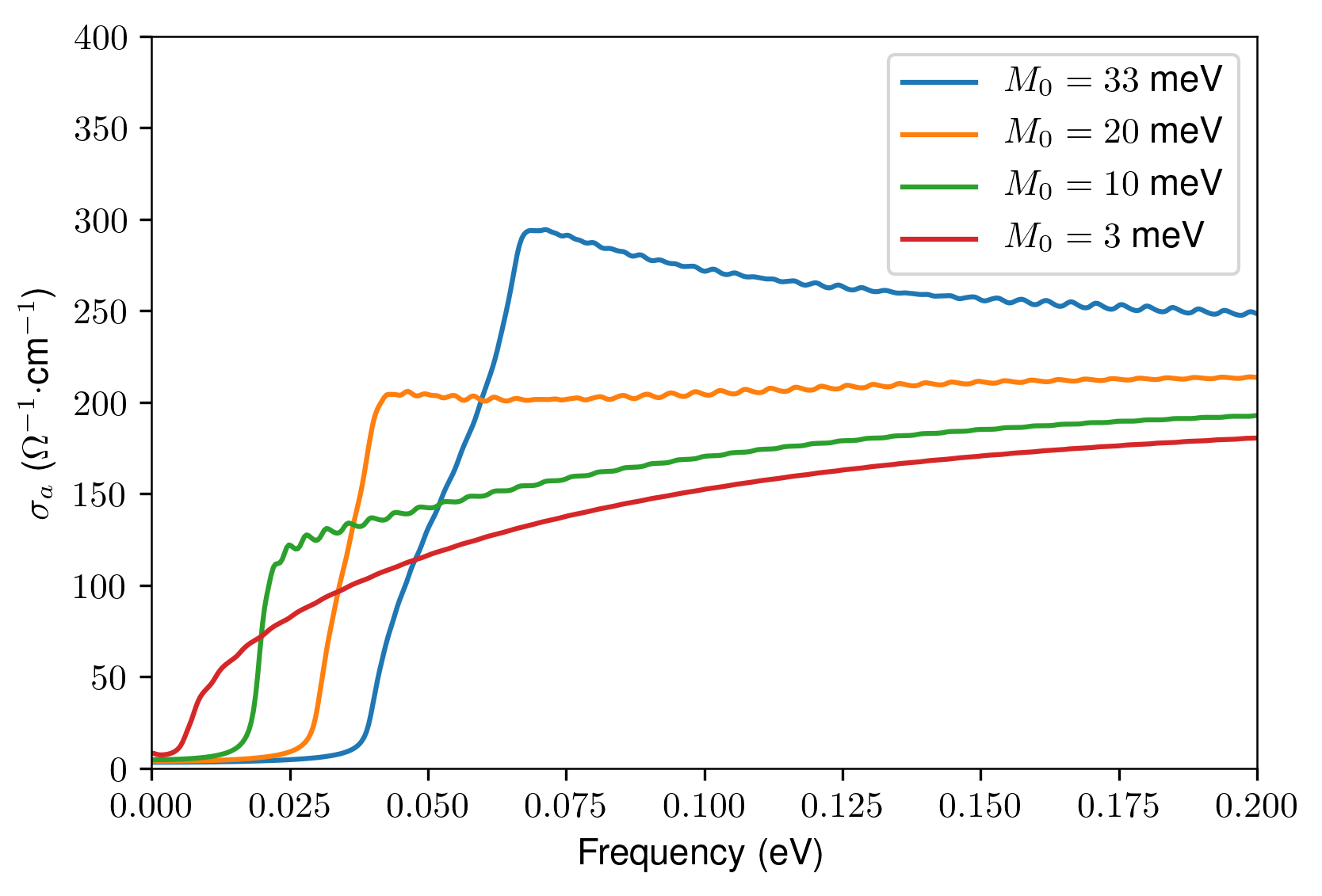
We calculated the optical conductivity along for four values of , ranging from 33 meV, which is the value given by DFT, to 3 meV, which matches the experimental gap in Martino et al. (2019). The results are displayed in Fig. 4. Lowering the gap has two main consequences: the overall magnitude is reduced, and the slope turns positive overall up to the peak close to eV. Moreover, it still gives an extrapolation towards a finite value at zero frequency, and therefore fits overall very well the experimental data. It also comes very close to the behaviour of the two-band model introduced in Martino et al. (2019), which goes as the square root of the frequency. The model we have put forward is thus a valid alternative to the one designed in Ref. Martino et al. (2019), and bridges between ab-initio calculations and experimental data.
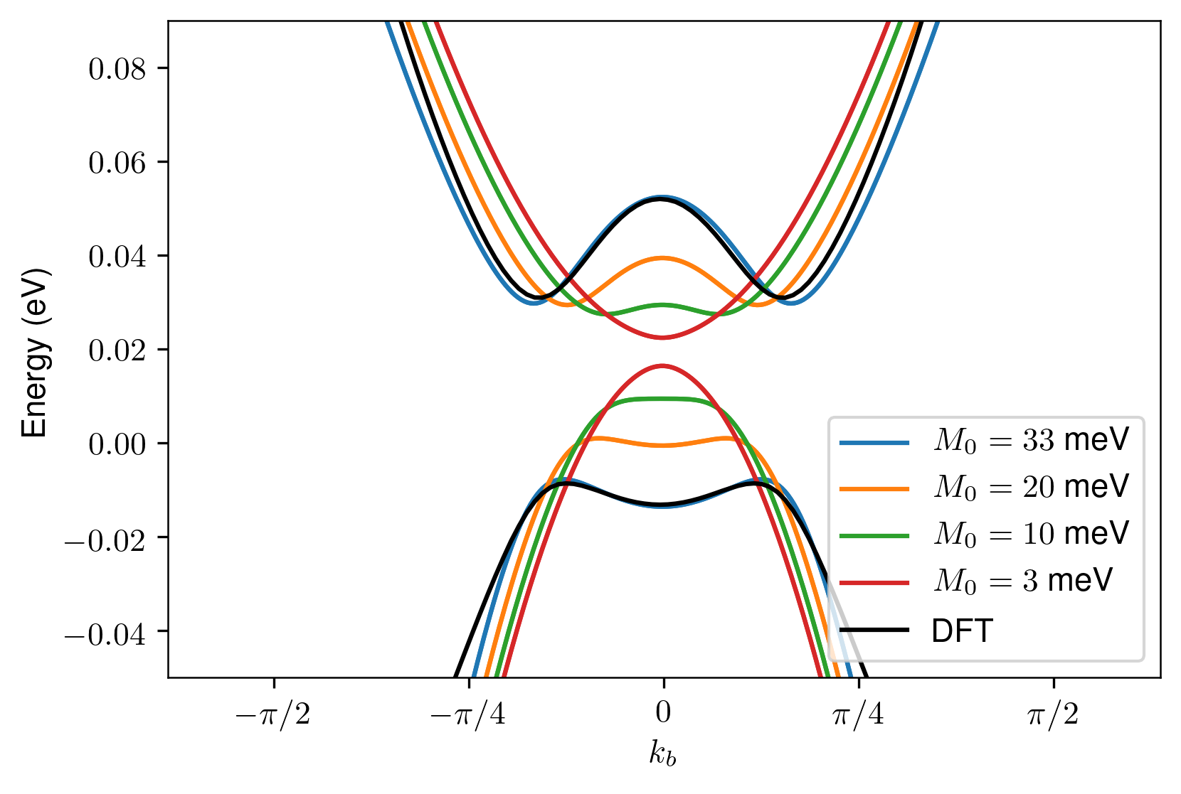
Further comparison is possible with ARPES data which established that the gap opens at precisely, that is with Xiong et al. (2017). This is unlike DFT results which, as discussed in Sec. II locate the gap on the segment , i.e. away from . This changes upon lowering to 3 meV when the shoulders in the bands along disappear and the gap has moved to the point (Fig. 5). This qualitative change of the shape of the spectrum can also be related to the qualitative change of shape of the optical conductivity upon changing .
VI Temperature dependence
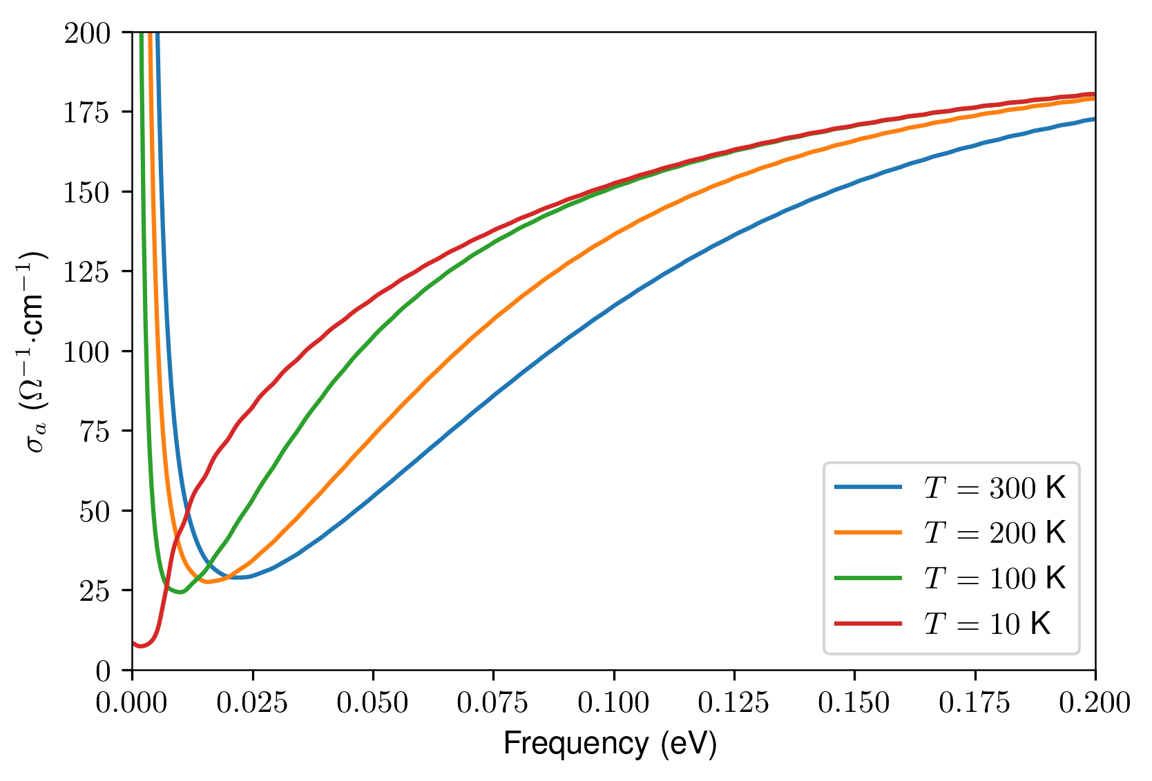
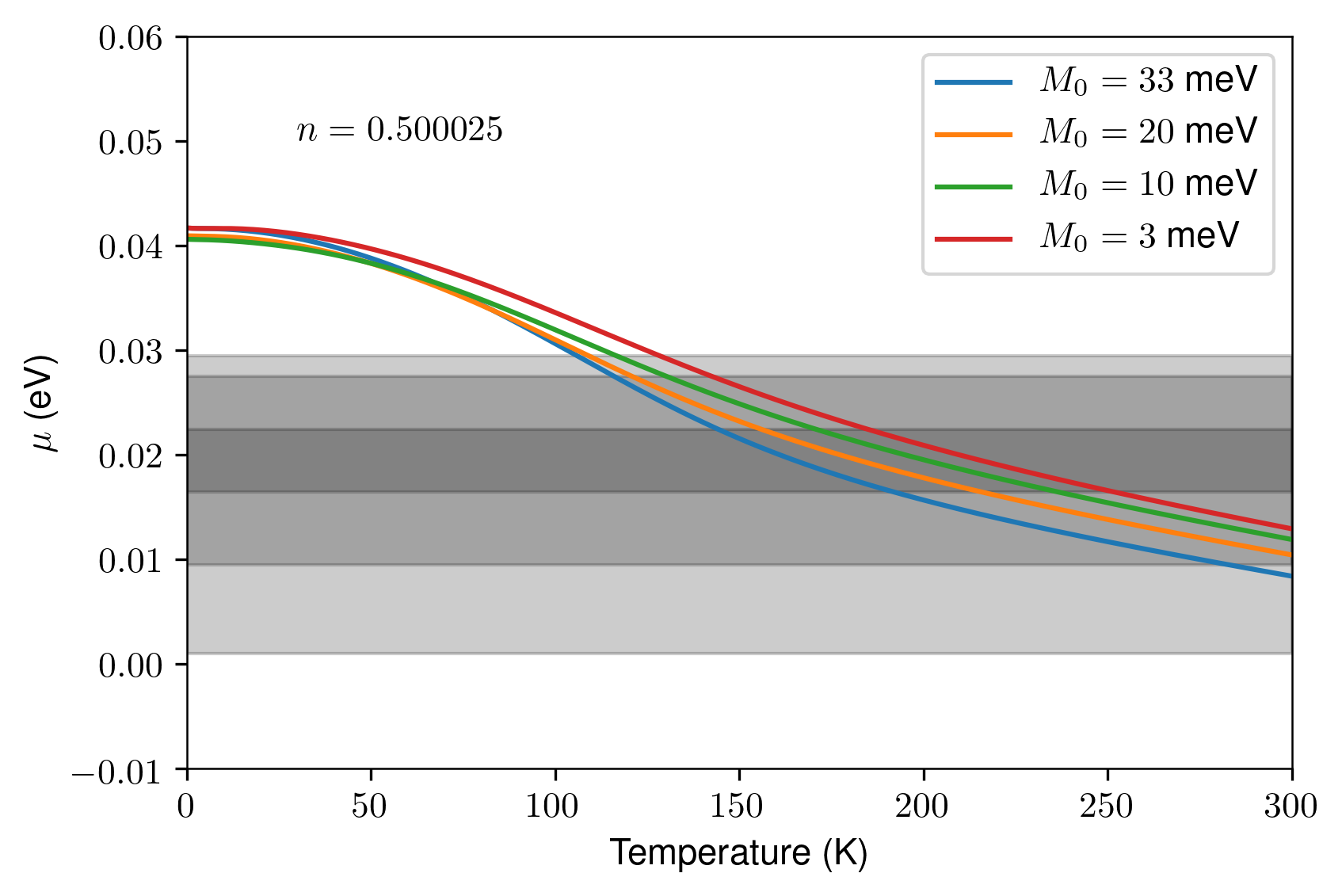
In order to cover a larger range of experimental data, we evaluated the temperature dependence with meV of the optical conductivity along (Fig. 6). Strikingly, for temperatures down to 100 K, has a sharp Drude peak at low frequency. This is surprising since we are considering a semiconductor with a nominal Fermi energy inside the gap. To understand this better, we calculated the temperature evolution of the chemical potential (Fig. 7). At half filling, crosses the top of the valence band close to 100 K, which explains the Drude peak above this temperature.
Moreover, we find that varies strongly with temperature, to the point that between 0 and 300 K it sweeps an energy window larger than the gap. This matches ARPES measurements showing a large drop of when raising temperature McIlroy et al. (2004); Manzoni et al. (2015); Xiong et al. (2017); Zhang et al. (2017), as well as NMR results Tian et al. (2019). In addition, it is consistent with reports of strong variation of the carrier density with temperature in optical conductivity Chen et al. (2015a) and Hall Tang et al. (2019) measurements. However, these experimental results are still being debated, since a raising of when raising temperature has also been measured using ARPES in some samples Moreschini et al. (2016); Wu et al. (2016). The difference with the measurements showing a lowering was related to variations in sample growth conditions Xiong et al. (2017).
This lowering of can also be seen as a change from - to -type carriers when raising the temperature. This was measured as a change of sign in the thermopower Jones et al. (1982); McIlroy et al. (2004); Shahi et al. (2018); Martino et al. (2019), concomitant with a peak in the resistivity, and thus interpreted as its origin. For this reason, we calculate the conductivity and resistivity as a function of temperature.
So far we considered the four-band model at half filling; converges towards the middle of the gap at zero temperature. This implies that the system is insulating at low temperature and will have a diverging resistivity in the limit of zero temperature, unlike most experimental results. We know however from ARPES experiments that in many samples the chemical potential does not lie inside the gap McIlroy et al. (2004); Manzoni et al. (2015); Li et al. (2016b); Moreschini et al. (2016); Wu et al. (2016); Xiong et al. (2017); Zhang et al. (2017) which was explained by -doping due to chemical vapor transport synthesis Shahi et al. (2018).
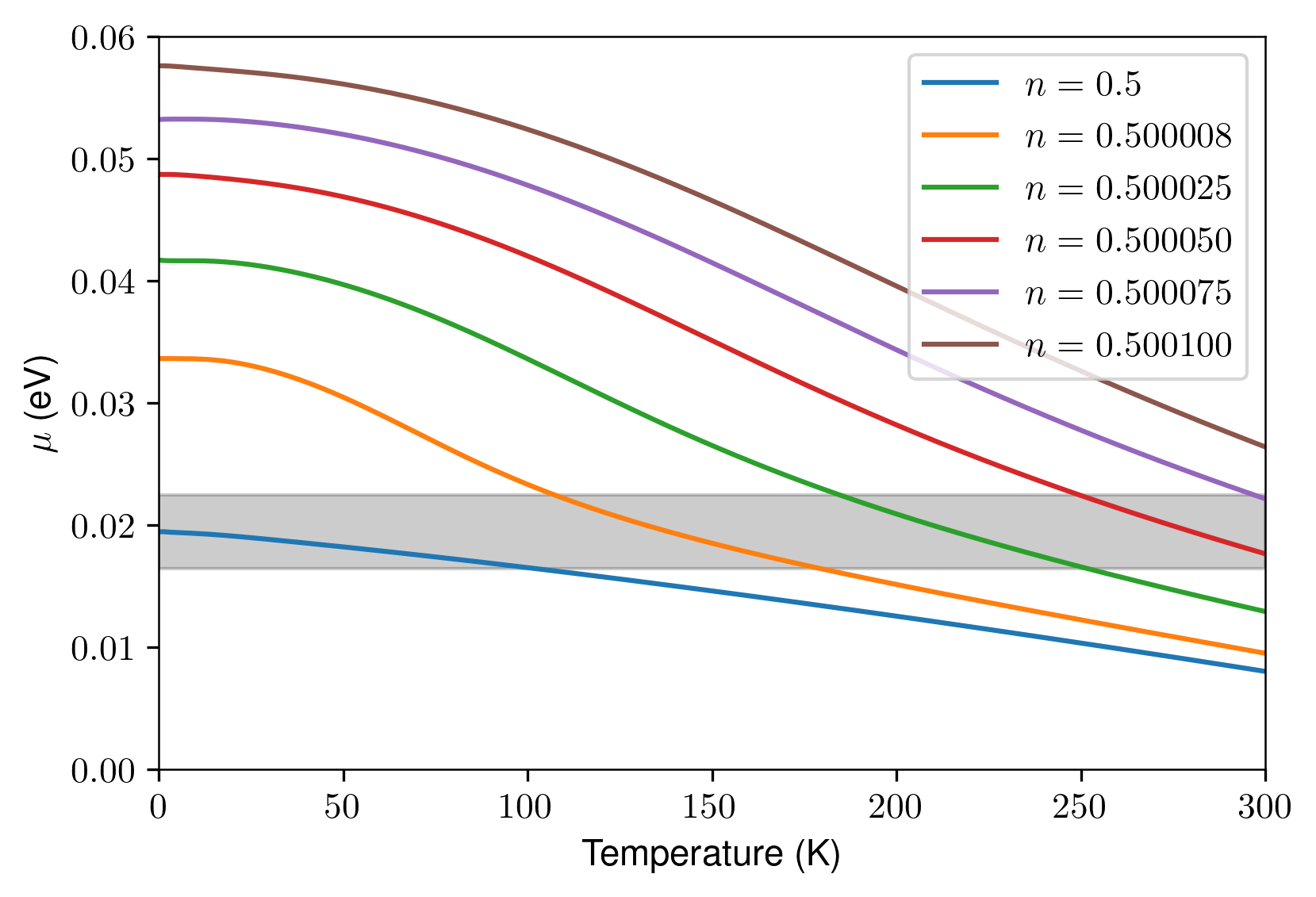
Our results for for different values of the filling are presented in Fig. 7. Already for a filling increase as small as from to , the chemical potential rises well above the gap towards zero temperature. Its change with temperature is also faster than in the half-filling case, it crosses the whole gap within less than 100 K and lies well below the valence band edge at 300 K. When raising the filling above , is shifted upwards and no longer enters the gap below 300 K and instead lies within the conduction band. This is particularly striking: ZrTe5 undergoes a transition from semiconductor to metal for a variation in filling of the order of ( cm-3), which is very small. This sheds light from a theoretical point of view on the strong variations in samples prepared with different synthesis methods Shahi et al. (2018).
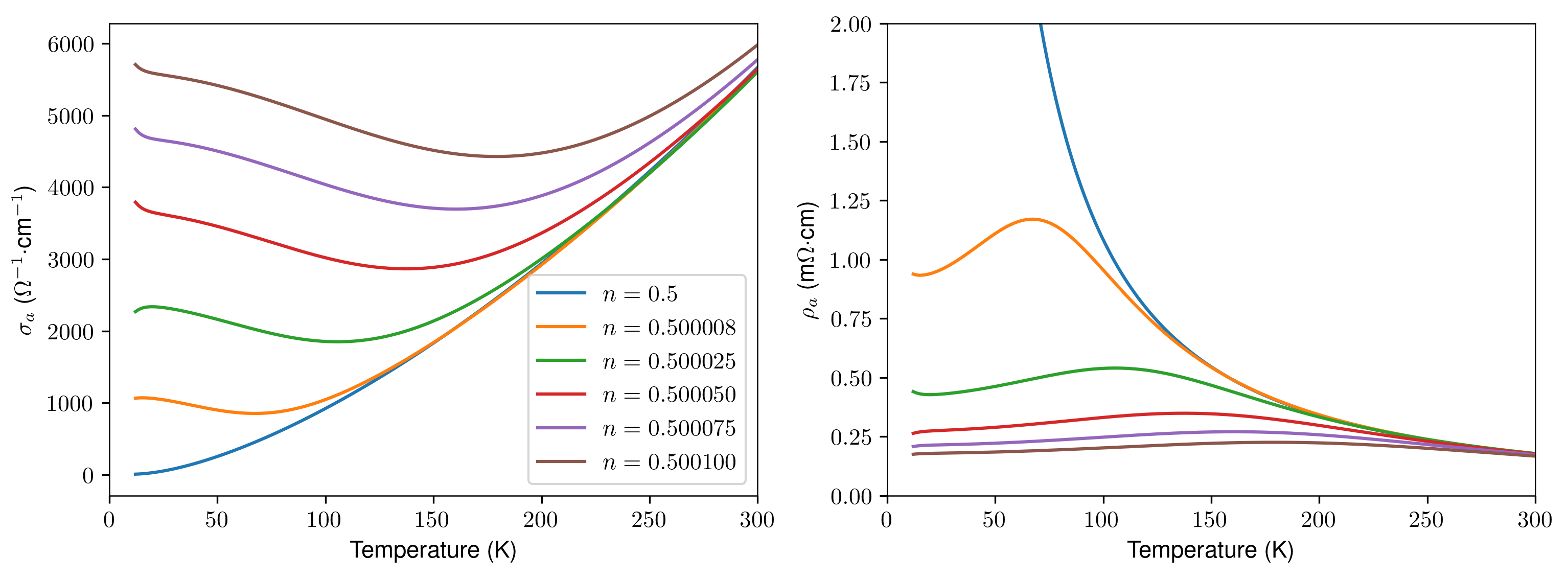
Results for the dc conductivity and the resistivity as a function of temperature for different values of the filling are collected in Fig. 8. As expected, the resistivity at half filling diverges at zero temperature. When raising the filling, the resistivity at zero temperatures turns finite and a peak develops at intermediate temperatures. Its height goes down and its position shifts to higher temperatures when raising the filling, clearly showing that the crossing of the gap, and therefore the variation of , is the cause of the resistivity peak.
The position of the resistivity peak is therefore a good comparison point between samples, as it is very sensitive to very small changes of filling. It has indeed been used as such in the literature, with samples in one study sometimes having resistivity peaks 50 K apart but with the same height Martino et al. (2019).
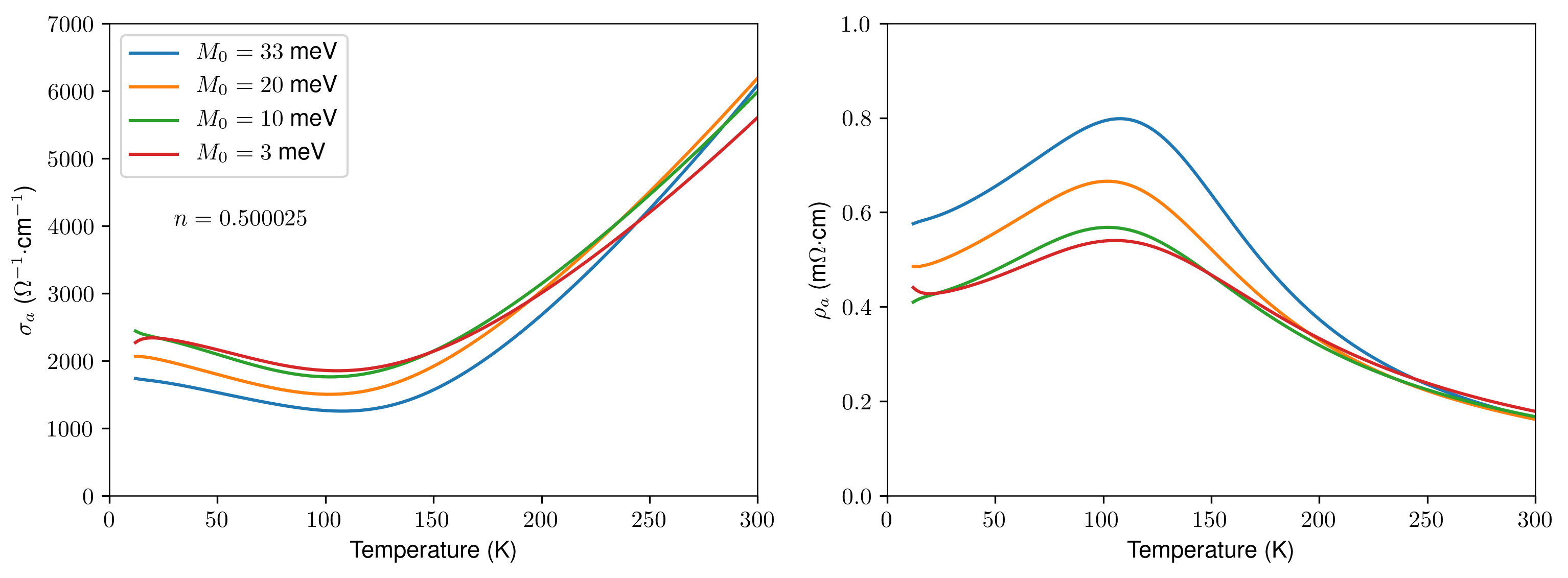
We single out one filling value in order to study the dependence of the peak on the gap. We choose to focus on , at which crosses the 6 meV gap entirely between approximately 190 K and 250 K. When the gap is raised, the temperature evolution of the chemical potential almost stays the same (Fig. 10), but the physics changes: for meV and above, the chemical potential does not reach the top of the valence band at 300 K.
The calculated temperature-dependent resistivity, displayed in Fig. 9, shows a prominent peak between 100 and 150 K. The peak temperature does neither correspond to the temperature at which the chemical potential enters the gap, nor to the temperature where it reaches the middle of the gap, but rather falls in between the two. This is due to the rise in resistivity being compensated by the broadening due to higher temperatures. The peak height increases with the gap from 0.5 mcm for meV to 0.8 mcm for meV. Experimental results show resistivity peaks at temperatures ranging from 60 K to 160 K whose maximum varies between 0.8 and 3 mcm Tritt et al. (1999); McIlroy et al. (2004); Chen et al. (2015a); Manzoni et al. (2015); Li et al. (2016b); Zheng et al. (2016); Li et al. (2018); Xu et al. (2018); Tian et al. (2019); Tang et al. (2019); Martino et al. (2019) with which our results are consistent. Note that the peak height depends on : a larger value for would decrease the height of the Drude peak and therefore increase the resistivity. The resistivity increases from 300 K down to the peak temperature by a factor between 3 and 4 depending on the gap, as observed experimentally Martino et al. (2019). It levels off towards zero temperature due to the temperature-independent residual scattering in the calculation of the conductivity. The zero-temperature limit increases both with decreasing filling and with increasing gap. The resistivity at very low temperature exhibits small down- or up-turns, related to the discrete k-point mesh used in the calculation, which becomes less fine than the sharp peaks in Eq. 6 for low enough temperature.
VII Conclusion
We derived a four-band model for ZrTe5 using theory, and fitted its parameters on the DFT band structure. Since ARPES results match DFT results except for the value of the gap Wu et al. (2016); Martino et al. (2019), we varied in the model to modify the electronic structure and in particular adjust the band gap to its experimental value, and left the other parameters untouched. The calculated optical conductivity corresponds well to experimental data Xu et al. (2018); Martino et al. (2019), showing that the model, as well as DFT calculations, are instrumental in describing the physics of ZrTe5 close to the Fermi level.
The chemical potential varies strongly with temperature, to the point that for fillings slightly above one half it crosses the gap entirely between zero and room temperature. The variation in filling needed to shift the chemical potential is very small, of the order of . This sheds light on how small variations in synthesis can cause large differences between samples with respect to their electronic conduction Shahi et al. (2018). The temperature-dependent resistivity for various values of the filling displays a prominent peak; its position, width, and amplitude are consistent with experimental data. Moreover, its position shifts with the filling, and therefore the chemical potential. This confirms theoretically the conclusions of key experiments which attributed the origin of the resistivity peak to the large shift of the chemical potential with temperature McIlroy et al. (2004); Manzoni et al. (2015); Xiong et al. (2017); Zhang et al. (2017); Xu et al. (2018); Tian et al. (2019). In particular, we obtain this resistivity peak without relying on a topological phase transition.
We have therefore, using a single model fitted on ab-initio results, successfully replicated three key experimental results on ZrTe5, namely the specific shape of the low frequency optical conductivity, the variation of the chemical potential with temperature and the peak in the temperature dependent resistivity. This renders this model a promising basis for addressing other exotic physics discovered in this material, such as its peculiar magnetotransport Liang et al. (2018).
Acknowledgements
We thank Daniel Braak, Liviu Chioncel, Andreas Östlin, Miloš M. Radonjić, Patrick Seiler, Alexey Shorikov and Yi Zhang for helpful discussions. This work was supported by the Deutsche Forschungsgemeinschaft — Grant number 107745057, TRR 80.
References
- Weng et al. (2014) H. Weng, X. Dai, and Z. Fang, Phys. Rev. X 4, 011002 (2014).
- Fan et al. (2017) Z. Fan, Q.-F. Liang, Y. B. Chen, S.-H. Yao, and J. Zhou, Scientific Reports 7, 45667 (2017).
- Monserrat and Narayan (2019) B. Monserrat and A. Narayan, arXiv e-prints , arXiv:1909.07613 (2019).
- Li et al. (2016a) X.-B. Li, W.-K. Huang, Y.-Y. Lv, K.-W. Zhang, C.-L. Yang, B.-B. Zhang, Y. B. Chen, S.-H. Yao, J. Zhou, M.-H. Lu, L. Sheng, S.-C. Li, J.-F. Jia, Q.-K. Xue, Y.-F. Chen, and D.-Y. Xing, Phys. Rev. Lett. 116, 176803 (2016a).
- Wu et al. (2016) R. Wu, J.-Z. Ma, S.-M. Nie, L.-X. Zhao, X. Huang, J.-X. Yin, B.-B. Fu, P. Richard, G.-F. Chen, Z. Fang, X. Dai, H.-M. Weng, T. Qian, H. Ding, and S. H. Pan, Phys. Rev. X 6, 021017 (2016).
- Moreschini et al. (2016) L. Moreschini, J. C. Johannsen, H. Berger, J. Denlinger, C. Jozwiak, E. Rotenberg, K. S. Kim, A. Bostwick, and M. Grioni, Phys. Rev. B 94, 081101 (2016).
- Xiong et al. (2017) H. Xiong, J. A. Sobota, S.-L. Yang, H. Soifer, A. Gauthier, M.-H. Lu, Y.-Y. Lv, S.-H. Yao, D. Lu, M. Hashimoto, P. S. Kirchmann, Y.-F. Chen, and Z.-X. Shen, Phys. Rev. B 95, 195119 (2017).
- Manzoni et al. (2016) G. Manzoni, L. Gragnaniello, G. Autès, T. Kuhn, A. Sterzi, F. Cilento, M. Zacchigna, V. Enenkel, I. Vobornik, L. Barba, F. Bisti, P. Bugnon, A. Magrez, V. N. Strocov, H. Berger, O. V. Yazyev, M. Fonin, F. Parmigiani, and A. Crepaldi, Phys. Rev. Lett. 117, 237601 (2016).
- Li et al. (2016b) Q. Li, D. E. Kharzeev, C. Zhang, Y. Huang, I. Pletikosić, A. Fedorov, R. Zhong, J. Schneeloch, G. Gu, and T. Valla, Nature Physics 12, 550 (2016b).
- Chen et al. (2015a) R. Y. Chen, S. J. Zhang, J. A. Schneeloch, C. Zhang, Q. Li, G. D. Gu, and N. L. Wang, Phys. Rev. B 92, 075107 (2015a).
- Yuan et al. (2016) X. Yuan, C. Zhang, Y. Liu, A. Narayan, C. Song, S. Shen, X. Sui, J. Xu, H. Yu, Z. An, J. Zhao, S. Sanvito, H. Yan, and F. Xiu, Npg Asia Materials 8, e325 (2016).
- Zheng et al. (2016) G. Zheng, J. Lu, X. Zhu, W. Ning, Y. Han, H. Zhang, J. Zhang, C. Xi, J. Yang, H. Du, K. Yang, Y. Zhang, and M. Tian, Phys. Rev. B 93, 115414 (2016).
- Qiu et al. (2016) G. Qiu, Y. Du, A. Charnas, H. Zhou, S. Jin, Z. Luo, D. Y. Zemlyanov, X. Xu, G. J. Cheng, and P. D. Ye, Nano Letters 16, 7364 (2016).
- Chen et al. (2015b) R. Y. Chen, Z. G. Chen, X.-Y. Song, J. A. Schneeloch, G. D. Gu, F. Wang, and N. L. Wang, Phys. Rev. Lett. 115, 176404 (2015b).
- Chen et al. (2017) Z.-G. Chen, R. Y. Chen, R. D. Zhong, J. Schneeloch, C. Zhang, Y. Huang, F. Qu, R. Yu, Q. Li, G. D. Gu, and N. L. Wang, Proceedings of the National Academy of Sciences 114, 816 (2017), https://www.pnas.org/content/114/5/816.full.pdf .
- Jiang et al. (2017) Y. Jiang, Z. L. Dun, H. D. Zhou, Z. Lu, K.-W. Chen, S. Moon, T. Besara, T. M. Siegrist, R. E. Baumbach, D. Smirnov, and Z. Jiang, Phys. Rev. B 96, 041101 (2017).
- Li et al. (2018) P. Li, C. H. Zhang, J. W. Zhang, Y. Wen, and X. X. Zhang, Phys. Rev. B 98, 121108 (2018).
- Jones et al. (1982) T. Jones, W. Fuller, T. Wieting, and F. Levy, Solid State Communications 42, 793 (1982).
- Skelton et al. (1982) E. Skelton, T. Wieting, S. Wolf, W. Fuller, D. Gubser, T. Francavilla, and F. Levy, Solid State Communications 42, 1 (1982).
- Tritt et al. (1999) T. M. Tritt, N. D. Lowhorn, R. T. Littleton, A. Pope, C. R. Feger, and J. W. Kolis, Phys. Rev. B 60, 7816 (1999).
- McIlroy et al. (2004) D. N. McIlroy, S. Moore, D. Zhang, J. Wharton, B. Kempton, R. Littleton, M. Wilson, T. M. Tritt, and C. G. Olson, Journal of Physics: Condensed Matter 16, L359 (2004).
- Manzoni et al. (2015) G. Manzoni, A. Sterzi, A. Crepaldi, M. Diego, F. Cilento, M. Zacchigna, P. Bugnon, H. Berger, A. Magrez, M. Grioni, and F. Parmigiani, Phys. Rev. Lett. 115, 207402 (2015).
- Zhang et al. (2017) Y. Zhang, C. Wang, L. Yu, G. Liu, A. Liang, J. Huang, S. Nie, X. Sun, Y. Zhang, B. Shen, J. Liu, H. Weng, L. Zhao, G. Chen, X. Jia, C. Hu, Y. Ding, W. Zhao, Q. Gao, C. Li, S. He, L. Zhao, F. Zhang, S. Zhang, F. Yang, Z. Wang, Q. Peng, X. Dai, Z. Fang, Z. Xu, C. Chen, and X. J. Zhou, Nature Communications 8, 15512 (2017).
- Martino et al. (2019) E. Martino, I. Crassee, G. Eguchi, D. Santos-Cottin, R. D. Zhong, G. D. Gu, H. Berger, Z. Rukelj, M. Orlita, C. C. Homes, and A. Akrap, Phys. Rev. Lett. 122, 217402 (2019).
- Lu et al. (2017) J. Lu, G. Zheng, X. Zhu, W. Ning, H. Zhang, J. Yang, H. Du, K. Yang, H. Lu, Y. Zhang, and M. Tian, Phys. Rev. B 95, 125135 (2017).
- Tang et al. (2018) F. Tang, P. Wang, P. Wang, Y. Gan, L. Wang, W. Zhang, and L. Zhang, Chinese Physics B 27, 087307 (2018).
- Li et al. (2019) Q. Li, Y. Lv, J. Wang, S. Bao, W. Shi, L. Zhu, W. Zhao, C. Xue, Z. Jia, L. Gao, Y. Chen, J. Wen, Y. Chen, and S. Li, Science China Physics, Mechanics & Astronomy 62, 967812 (2019).
- Nair et al. (2018) N. L. Nair, P. T. Dumitrescu, S. Channa, S. M. Griffin, J. B. Neaton, A. C. Potter, and J. G. Analytis, Phys. Rev. B 97, 041111 (2018).
- Xu et al. (2018) B. Xu, L. X. Zhao, P. Marsik, E. Sheveleva, F. Lyzwa, Y. M. Dai, G. F. Chen, X. G. Qiu, and C. Bernhard, Phys. Rev. Lett. 121, 187401 (2018).
- Tian et al. (2019) Y. Tian, N. Ghassemi, and J. H. Ross, Phys. Rev. B 100, 165149 (2019).
- Fu et al. (2020) B. Fu, H.-W. Wang, and S.-Q. Shen, “Dirac polarons and resistivity anomaly in zrte5 and hfte5,” (2020), arXiv:2007.08700 [cond-mat.mes-hall] .
- Shahi et al. (2018) P. Shahi, D. J. Singh, J. P. Sun, L. X. Zhao, G. F. Chen, Y. Y. Lv, J. Li, J.-Q. Yan, D. G. Mandrus, and J.-G. Cheng, Phys. Rev. X 8, 021055 (2018).
- Wang and Li (2020) Y.-X. Wang and F. Li, Phys. Rev. B 101, 195201 (2020).
- Rukelj et al. (2020) Z. Rukelj, C. C. Homes, M. Orlita, and A. Akrap, “Distinguishing the gapped and weyl semimetal scenario in zrte5: insights from an effective two-band model,” (2020), arXiv:2005.14582 [cond-mat.mes-hall] .
- Perdew et al. (1996) J. P. Perdew, K. Burke, and M. Ernzerhof, Phys. Rev. Lett. 77, 3865 (1996).
- Fjellvåg and Kjekshus (1986) H. Fjellvåg and A. Kjekshus, Solid State Communications 60, 91 (1986).
- Giannozzi et al. (2009) P. Giannozzi, S. Baroni, N. Bonini, M. Calandra, R. Car, C. Cavazzoni, D. Ceresoli, G. L. Chiarotti, M. Cococcioni, I. Dabo, A. Dal Corso, S. de Gironcoli, S. Fabris, G. Fratesi, R. Gebauer, U. Gerstmann, C. Gougoussis, A. Kokalj, M. Lazzeri, L. Martin-Samos, N. Marzari, F. Mauri, R. Mazzarello, S. Paolini, A. Pasquarello, L. Paulatto, C. Sbraccia, S. Scandolo, G. Sclauzero, A. P. Seitsonen, A. Smogunov, P. Umari, and R. M. Wentzcovitch, J. Phys. Condens. Matter 21, 395502 (2009).
- Elk (2004) “http://elk.sourceforge.net,” (2004).
- Pizzi et al. (2019) G. Pizzi, V. Vitale, R. Arita, S. Blügel, F. Freimuth, G. Géranton, M. Gibertini, D. Gresch, C. Johnson, T. Koretsune, J. Ibañez-Azpiroz, H. Lee, J. Lihm, D. Marchand, A. Marrazzo, Y. Mokrousov, J. I. Mustafa, Y. Nohara, Y. Nomura, L. Paulatto, S. Poncé, T. Ponweiser, J. Qiao, F. Thöle, S. S. Tsirkin, M. Wierzbowska, N. Marzari, D. Vanderbilt, I. Souza, A. A. Mostofi, and J. R. Yates, arXiv e-prints , arXiv:1907.09788 (2019), arXiv:1907.09788 [cond-mat.mtrl-sci] .
- Wu et al. (2018) Q. Wu, S. Zhang, H.-F. Song, M. Troyer, and A. A. Soluyanov, Computer Physics Communications 224, 405 (2018).
- Hedin and Lundqvist (1969) L. Hedin and S. O. Lundqvist, “Effects of electron-electron and electron-phonon interactions on the one-electron states of solids,” in Solid State Physics, Vol. 23, edited by F. Seitz, D. Turnbull, and H. Ehrenreich (Academic Press, 1969) pp. 1–181.
- Becke (1993) A. D. Becke, The Journal of Chemical Physics 98, 5648 (1993).
- Heyd et al. (2003) J. Heyd, G. E. Scuseria, and M. Ernzerhof, The Journal of Chemical Physics 118, 8207 (2003).
- Gresch (2018) D. Gresch, Identifying Topological Semimetals, Ph.D. thesis, ETH Zürich (2018).
- Nechaev and Krasovskii (2016) I. A. Nechaev and E. E. Krasovskii, Phys. Rev. B 94, 201410 (2016).
- Choi et al. (2020) Y. Choi, J. W. Villanova, and K. Park, Phys. Rev. B 101, 035105 (2020).
- Tkachov (2016) G. Tkachov, Topological Insulators (Jenny Stanford Publishing, New York, 2016).
- Yang et al. (2019) P. Yang, W. Wang, X. Zhang, K. Wang, L. He, W. Liu, and Y. Xu, Scientific Reports 9, 3558 (2019).
- Tang et al. (2019) F. Tang, Y. Ren, P. Wang, R. Zhong, J. Schneeloch, S. A. Yang, K. Yang, P. A. Lee, G. Gu, Z. Qiao, and L. Zhang, Nature 569, 537 (2019).
- Liang et al. (2018) T. Liang, J. Lin, Q. Gibson, S. Kushwaha, M. Liu, W. Wang, H. Xiong, J. A. Sobota, M. Hashimoto, P. S. Kirchmann, Z.-X. Shen, R. J. Cava, and N. P. Ong, Nature Physics 14, 451 (2018).