Realization of the square-root higher-order topological insulator in electric circuits
keywords:
American Chemical Society, LaTeXUniversity of Electronic Science and Technology of China] School of Electronic Science and Engineering and State Key Laboratory of Electronic Thin Films and Integrated Devices, University of Electronic Science and Technology of China, Chengdu 610054, China \abbreviationsIR,NMR,UV \captionsetup[figure]labelfont=bf,name=Figure,labelsep=period Abstract: Higher-order topological insulator (HOTI) represents a new phase of matter, the characterization of which goes beyond the conventional bulk-boundary correspondence and is attracting significant attention by the broad community. Using a square-root operation, it has been suggested that a square-root HOTI may emerge in a hybrid honeycomb-kagome lattice. Here, we report the first experimental realization of the square-root HOTI in topological LC circuits. We show theoretically and experimentally that the square-root HOTI inherits the feature of wave function from its parent, with corner states pinned to non-zero energies. The topological feature is fully characterized by the bulk polarization. To directly measure the finite-energy corner modes, we introduce extra grounded inductors to each node. Our results experimentally substantiate the emerging square-root HOTI and pave the way to realizing exotic topological phases that are challenging to observe in condensed matter physics.
KEYWORDS: higher-order topological insulator, square-root operation, honeycomb-kagome lattice, electrical circuit
1 Introduction
Topological insulators manifest unique and often counterintuitive properties, such as the robust electron transport and wave propagation against defects and disorder 1, 2, 3, which are appealing for quantum computing interface 4, 5 and nonreciprocal lasing 6, 7, 8, 9. Conventional topological insulators support chiral edge states of codimension one. In contrast, the emerging higher-order topological insulator (HOTI) allows topologically non-trivial boundary states with codimension larger than one 10, 11, 12, 13, thus shifting the standard paradigm of bulk-boundary correspondence. The realization of HOTIs has been reported in variety of fields, such as photonics 14, 15, 16, 17, 18, 19, 20, 21, 22, acoustics 23, 24, 25, 26, 27, 28, 29, 30, mechanics 31, 32, and recently spintronics 33, 34, 35. Using a square-root operation, Arkinstall et al. proposed a pathway to design a new type of topological material, the so-called square-root topological insulator, which inherits the nontrivial nature of Bloch wave function from its parent Hamiltonian 36. The approach is analogous to the case that Dirac discovered the positron when he took the square root of the Klein-Gordon equation for relativistic particles 37. Photonic experiments indeed confirm the square-root topological insulator 38. Very recently, Mizoguchi et al. generalized the idea to HOTI by showing that the square-root HOTI may emerge in a decorated honeycomb lattice 39. However, the experimental realization of squre-root HOTI is still missing.
It has been shown that electrical circuits can act as a powerful platform to realize topological states 40, 41, 42, 43, 44, 45 that are challenging to observe in condensed matter experiments. Here, we demonstrate the square-root HOTI in two-dimensional LC circuits arranged in a hybrid honeycomb-kagome (HK) manner [see Figure 1a]. We show theoretically and experimentally that the square-root HOTI inherits features from its parent, with the topology being fully characterized by the bulk polarization. We find that the emerging corner states are pinned to finite energies, so that they cannot be directly observed by impedance measurements, in contrast to their “zero-energy" counterpart in normal HOTIs 41, 44. To overcome this issue, we introduce extra grounded inductors, which shift the “non zero-energy" corner modes to zero energy without modifying their wave functions.
2 Results and discussion
2.1 Honeycomb-kagome electrical circuit
We consider a lossless linear electric circuit consisting of capacitors and inductors and label the nodes of the circuit using . The responses of the circuit at frequency obey Kirchhoff’s law
| (1) |
where is the external current flowing into node , is the voltage of node , and () is the circuit Laplace operator
| (2) |
with the capacitance between nodes and and being the grounding inductance of node .
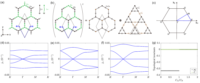
Figure 1a shows the structure of an infinite HK circuit, the squared Hamiltonian of which can be viewed as the direct sum of the Hamiltonians of a honeycomb and a breathing-kagome circuits (see analysis below), as illustrated in Figure 1b. The unit cell including five nodes is represented by the dashed black rhombus. and are the two basis vectors with being the lattice constant. Figure 1c displays the first Brillouin zone (BZ). The Hamiltonian of the circuit can be written as
| (3) |
with matrix elements
| (4) | ||||
with the wave vector. By properly selecting , , , and , i.e., , the diagonal elements of the Hamiltonian vanish at resonance. The Hamiltonian then can be simplified to
| (5) |
where and are the and zero matrix, respectively, and is the matrix
| (6) |
The Hamiltonian (5) is chiral-symmetric, because meets the condition with
| (7) |
where and represent the and identity matrix, respectively. This indicates the existence of the parent Hamiltonian whose square root gives 36, 39. Indeed, one can obtain the eigenvalues of by taking its square
| (8) |
where and represent the Hamiltonian of a honeycomb sublattice with staggered on-site potentials and a breathing kagome sublattice, respectively, as plotted in Figure 1b. The dispersion relation then can be conveniently computed by solving (8): for and for with , and taking a square-root operation afterwards. The band structures for different capacitance ratios are shown in Figures 1d-1f, which is gapped at point for . It is therefore possible to realize the TI phase due to the gap opening. Interestingly, we find that the solution indicates a flat band. As shown in Figures 1d-1f, the peculiar flat band touches other dispersive bands, which is an ideal system to study the noncontractible loop state and the topologically protected band-touching 46.
The first-order topological insulator phase can be determined by computing the topologically invariant Chern number 47, 48
| (9) |
where is the projection matrix , with being the normalized eigenstates of Eq. (3) in any band, and the integral is over the first BZ.
In order to judge the existence of HOTI, we can employ the bulk polarization as a topological invariant. For symmetric systems, the bulk polarization for the th band can be written as 24, 49
| (10) |
where with the th eigenvector . The -matrix is expressed as
| (11) |
Here, we are interested in the 5th band. As shown in Figure 1g, takes for , and 0 for . A topological phase transition occurs at . Meanwhile, the Chern number vanishes for all , indicating that the system does not support the first-order TI phase. We thus conclude that the system allows only two topologically distinct phases for and .
2.2 Corner states
We consider a finite-size HK circuit with nodes, as depicted in Figure 2a. The circuit Laplacian reads
| (12) |
with and .
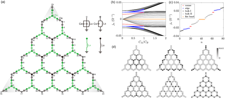
By diagonalizing (12), we obtain both eigenvalues (admittances) and eigenfunctions with . In Figure 2b, we display the admittance spectrum for ranging from 0 to 2. The HOTI phase only appears for (the red line segments). In Figure 2c, we exhibit a representative example at , where the red, blue, black, gray, and orange dots represent the corner, edge, bulk I, bulk II, and flat-band states, respectively. We set nF and H in the calculation if not stated otherwise. It can be clearly seen that two groups of three-fold degenerate modes (red dots) are in the band gap, indicating the corner states. The spatial distribution of wave functions are plotted in Figure 2d, from which we can distinguish these modes. Bulk II is spatially more extended than bulk I. In addition, we observe two kinds of flat-band modes: one lies in the kagome sublattice and the other one localizes in the honeycomb sublattice, in contrast to the infinity HK lattice, where flat-band states only appear in the kagome sublattice 46.
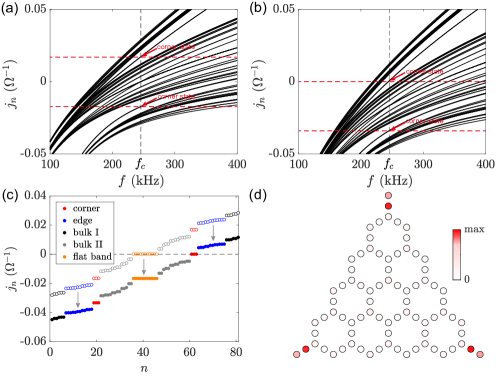
Figure 3a shows the theoretical spectrum of the circuit Laplacian as a function of the driving frequency, where two isolated bands localize in the gap of the spectrum, representing the corner states. We note that the corner states in our system are not at the “zero energy" as the ones in the normal HOTI circuit 44, as plotted in Figures 2c and 3a. One therefore cannot detect the corner states through a direct two-point impedance measurement. To solve this problem, we connect grounded inductors to all nodes to shift the whole spectrum down and move the corner modes to the zero energy, as shown in Figure 3b, whereas the relative positions of the corner, edge, bulk and flat-band states do not change. Diagonalizing (12) with , i.e., adding to each diagonal element of matrix , we obtain the modified eigenvalues (admittances) and find that the corner states indeed emerge at the zero energy (the solid red dots), as plotted in Figure 3c. Figure 3d shows the spatial distribution of the impedance for the corner state. In the theoretical calculations, we adopt H.
2.3 Experimental observation
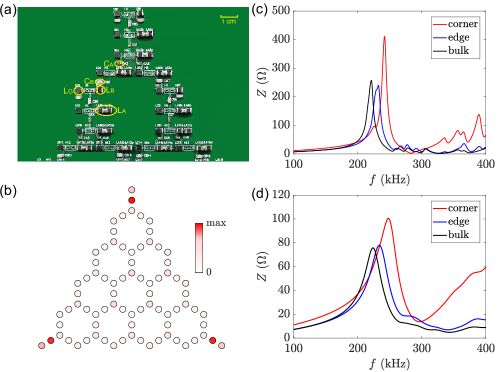
The electric circuits are fabricated on a printed circuit board as shown in Figure 4a. We choose electric elements nF, H, and H. The resonant frequency is given by kHz. It is noted that the inductance of decays slightly with the increasing of the driving frequency, with the mean value 14 H near . First of all, we measure the distribution of impedance in this circuit by the Impedance Analyzer (Keysight E4990A) [see Figure 4b], which is in good agreement with the theoretical result in Figure 3d. We then determine the impedance between three representative nodes and the ground as a function of the driving frequency, plotted in Figure 4c (theory) and Figure 4d (experiment), where we choose 2nd, 33th, and 34th nodes to quantify the signals from the corner, bulk, and edge states, respectively. In the theoretical calculation, we have averaged the result after realizations of uniformly distributed disorder (we assume a tolerance of each electric element). Both the theoretical and experimental (red) curves display a strong peak at the resonant frequency , which confirms the very existence of the corner state.
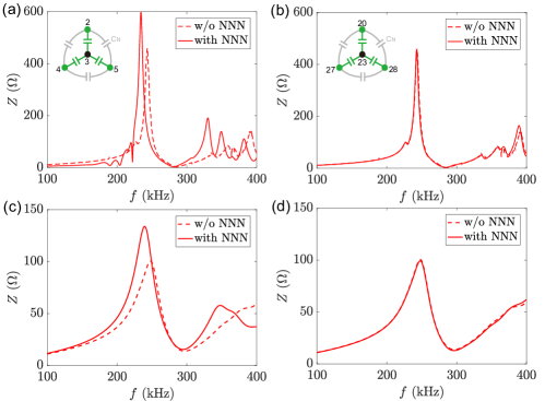
To examine the robustness of the corner states, we introduce two kinds of next-nearest-neighbor (NNN) hopping terms to the system by connecting extra capacitors nF with the configurations shown in the insets of Figures 5a and 5b. When we connect 2nd, 4th, and 5th nodes [see Figure 2a for numbered nodes] that breaks the chiral symmetry, the peak of zero mode suffers a blueshift about kHz, as depicted in Figures 5a and 5c. However, when we introduce NNN hopping in the deep bulk, by connecting 20th, 27th, and 28th nodes, the corner state remains at the same frequency because of the chiral symmetry conserving, as shown in Figures 5b and 5d. Experimental results agree well with theoretical calculations.
3 Conclusion
To summarize, we presented an experimental realization of the square-root HOTI in LC circuits. We demonstrated theoretically and experimentally that the square-root HOTIs inherit the feature of wave function from their parent. The emerging corner states are pinned to non-zero energies with topological features being fully characterized by the bulk polarization. To directly measure the finite-energy corner modes, we introduce extra grounded inductors to each node, thus shifting the localized modes to zero energy without modifying their wave distributions. Our results substantiate the emerging square-root HOTI and pave the way to observing exotic topological phases that are challenging to implement in condensed matter system.
4 Acknowledgement
This work was supported by the National Natural Science Foundation of China (Grants No. 11604041 and 11704060), and the National Key Research Development Program under Contract No. 2016YFA0300801.
5 Abbreviation
HOTI, Higher-order topological insulator; LC, inductors and capacitors; HK, honeycomb-kagome; BZ, Brillouin zone; NNN, next-nearest-neighbor.
6 Author information
6.1 Corresponding Authors
Peng Yan - School of Electronic Science and Engineering and State Key Laboratory of Electronic Thin Films and Integrated Devices, University of Electronic Science and Technology of China, Chengdu 610054 China; Email: yan@uestc.edu.cn
6.2 Authors
Lingling Song - School of Electronic Science and Engineering and State Key Laboratory of Electronic Thin Films and Integrated Devices, University of Electronic Science and Technology of China, Chengdu 610054, China
Huanhuan Yang - School of Electronic Science and Engineering and State Key Laboratory of Electronic Thin Films and Integrated Devices, University of Electronic Science and Technology of China, Chengdu 610054, China
Yunshan Cao - School of Electronic Science and Engineering and State Key Laboratory of Electronic Thin Films and Integrated Devices, University of Electronic Science and Technology of China, Chengdu 610054, China
6.3 Author Contributions
Peng Yan and Lingling Song conceived the idea and contributed to the project design. Lingling Song developed the theory and wrote the maniscript. Huanhuan Yang designed the circuits and performed the measurements. All authors discussed the results and revised the manuscript.
6.4 Notes
The authors declare no competing financial interest.
References
- 1 Hasan, M. Z.; Kane, C. L. Colloquium: Topological insulators. Rev. Mod. Phys. 2010, 82, 3045.
- 2 Qi, X.-L.; Zhang S.-C. Topological insulators and superconductors. Rev. Mod. Phys. 2011, 83, 1057.
- 3 Bernevig, B. A.; Hughes, T. L. Topological Insulators and Topological Superconductors. (Princeton University Press, 2013).
- 4 Barik, S.; Karasahin, A.; Flower, C.; Cai, T.; Miyake, H.; DeGottardi, W.; Hafezi, M.; Waks, E. A topological quantum optics interface. Science 2018, 359 (6376), 666-668.
- 5 Kitaev, A. Y. Unpaired Majorana fermions in quantum wires. Phys. Usp. 2001, 44, 131.
- 6 Bahari, B.; Ndao, A.; Vallini, F.; Amili, A. E.; Fainman, Y.; Kanté, B. Nonreciprocal lasing in topological cavities of arbitrary geometries. Science 2017, 358 (6363), 636-640.
- 7 Bandres, M. A.; Wittek, S.; Harari, G.; Parto, M.; Ren, J.; Segev, M.; Christodoulides, D. N.; Khajavikhan, M. Topological insulator laser: Experiments. Science 2018, 359 (6381), eaar4005.
- 8 Harari, G.; Bandres, M. A.; Lumer, Y.; Rechtsman, M. C.; Chong, Y. D.; Khajavikhan, M.; Christodoulides, D. N.; Segev, M. Topological insulator laser: Theory. Science 2018, 359 (6381), eaar4003.
- 9 St-Jean, P.; Goblot, V.; Galopin, E.; Lemaître, A.; Ozawa, T.; Gratiet, L. L.; Sagnes, I.; Bloch, J.; Amo, A. Lasing in topological edge states of a one-dimensional lattice. Nat. Photon. 2017, 11, 651-656.
- 10 Benalcazar, W. A.; Bernevig, B. A.; Hughes, T. L. Quantized electric multipole insulators. Science 2017 (6346), 357, 61-66.
- 11 Benalcazar, W. A.; Bernevig, B. A.; Hughes, T. L. Electric multipole moments, topological multipole moment pumping, and chiral hinge states in crystalline insulators. Phys. Rev. B 2017, 96, 245115.
- 12 Song, Z.; Fang, Z.; Fang, C. -Dimensional Edge States of Rotation Symmetry Protected Topological States. Phys. Rev. Lett. 2017, 119, 246402.
- 13 Ezawa, M. Higher-Order Topological Insulators and Semimetals on the Breathing Kagome and Pyrochlore Lattices. Phys. Rev. Lett. 2018, 120, 026801.
- 14 Xie, B.-Y.; Wang, H.-F.; Wang, H.-X.; Zhu, X.-Y.; Jiang, J.-H.; Lu, M.-H.; Chen, Y.-F. Second-order photonic topological insulator with corner states. Phys. Rev. B 2018, 98, 205147.
- 15 Noh, J.; Benalcazar, W. A.; Huang, S.; Collins, M. J.; Chen, K. P.; Hughes, T. L.; Rechtsman, M. C. Topological protection of photonic mid-gap defect modes. Nat. Photon. 2018, 12, 408-415.
- 16 Hassan, A. E.; Kunst, F. K.; Moritz, A.; Andler, G.; Bergholtz, E. J.; Bourennane, M. Corner states of light in photonic waveguides. Nat. Photon. 2019, 13, 697-700.
- 17 Mittal, S.; Orre, V. V.; Zhu, G.; Gorlach, M. A.; Poddubny, A.; Hafezi, M. Photonic quadrupole topological phases. Nat. Photon. 2019, 13, 692-696.
- 18 Chen, X.-D.; Deng, W.-M.; Shi, F.-L.; Zhao, F.-L.; Chen, M.; Dong, J.-W. Direct Observation of Corner States in Second-Order Topological Photonic Crystal Slabs. Phys. Rev. Lett. 2019, 122, 233902.
- 19 Xie, B.-Y.; Su, G.-X.; Wang, H.-F.; Su, H.; Shen, X.-P.; Zhan, P.; Lu, M.-H.; Wang, Z.-L.; Chen, Y.-F. Visualization of Higher-Order Topological Insulating Phases in Two-Dimensional Dielectric Photonic Crystals. Phys. Rev. Lett. 2019, 122, 233903.
- 20 Ota, Y.; Liu, F.; Katsumi, R.; Watanabe, K.; Wakabayashi, K.; Arakawa, Y.; Iwamoto, S. Photonic crystal nanocavity based on a topological corner state. Optica 2019, 6 (6), 786-789.
- 21 Zhang, L.; Yang, Y.; Lin, Z.-K.; Qin, P.; Chen, Q.; Gao, F.; Li, E.; Jiang, J.-H.; Zhang, B.; Chen, H. Higher-order photonic topological states in surface-wave photonic crystals. Adv. Sci. 2020, 7 (6), 1902724.
- 22 Li, M.; Zhirihin, D.; Filonov, D.; Ni, X.; Slobozhanyuk, A.; Alù, A.; Khanikaev, A. B. Photonic higher-order topological states induced by long range interactions. arXiv:1909.09199.
- 23 Xue, H.; Yang, Y.; Gao, F.; Chong, Y.; Zhang, B. Acoustic higher-order topological insulator on a kagome lattice. Nat. Mater. 2019, 18, 108-112.
- 24 Ni, X.; Weiner, M.; Alù, A.; Khanikaev, A. B. Observation of higher-order topological acoustic states protected by generalized chiral symmetry. Nat. Mater. 2019, 18, 113-120.
- 25 Xue, H.; Yang, Y.; Liu, G.; Gao, F.; Chong, Y.; Zhang, B. Realization of an Acoustic Third-Order Topological Insulator. Phys. Rev. Lett. 2019, 122, 244301.
- 26 He, C.; Yu, S.-Y.; Wang, H.; Ge, H.; Ruan, J.; Zhang, H.; Lu, M.-H.; Chen, Y.-F. Hybrid Acoustic Topological Insulator in Three Dimensions. Phys. Rev. Lett. 2019, 123, 195503.
- 27 Zhang, X.; Wang, H.-X.; Lin, Z.-K.; Tian, Y.; Xie, B.; Lu, M.-H.; Chen, Y.-F.; Jiang, J.-H.; Second-order topology and multidimensional topological transitions in sonic crystals. Nat. Phys. 2019, 15, 582-588.
- 28 Chen, Z.-G.; Xu, C.; Jahdali, R. A.; Mei, J.; Wu, Y. Corner states in a second-order acoustic topological insulator as bound states in the continuum. Phys. Rev. B 2019, 100, 075120.
- 29 Zhang, Z.; López, M. R.; Cheng, Y.; Liu, X.; Christensen, J. Non-Hermitian Sonic Second-Order Topological Insulator. Phys. Rev. Lett. 2019, 122, 195501.
- 30 Zhang, Z.; Long, H.; Liu, C.; Shao, C.; Cheng, Y.; Liu, X.; Christensen, J. Deep-Subwavelength Holey Acoustic Second-Order Topological Insulators. Adv. Mater. 2019, 31 (49), 1904682.
- 31 Serra-Garcia, M.; Peri, V.; Süsstrunk, R.; Bilal, O. R.; Larsen, T.; Villanueva, L. G.; Huber, S. D. Observation of a phononic quadrupole topological insulator Nature (London) 2018, 555, 342-345.
- 32 Fan, H.; Xia, B.; Tong, L.; Zheng, S.; Yu, D. Elastic Higher-Order Topological Insulator with Topologically Protected Corner States Phys. Rev. Lett. 2019, 122, 204301.
- 33 Li, Z.-X.; Cao, Y.; Yan, P.; Wang, X. R. Higher-order topological solitonic insulators. npj Comput. Mater. 2019, 5, 107.
- 34 Li, Z.-X.; Cao, Y.; Wang, X. R.; Yan, P. Symmetry-Protected Zero Modes in Metamaterials Based on Topological Spin Texture. Phys. Rev. Applied 2020, 13, 064058.
- 35 Li, Z.-X.; Cao, Y.; Wang, X. R.; Yan, P. Second-order topological solitonic insulator in a breathing square lattice of magnetic vortices. Phys. Rev. B 2020, 122, 204301.
- 36 Arkinstall, J.; Teimourpour, M. H.; Feng, L.; El-Ganainy, R.; Schomerus, H. Topological tight-binding models from nontrivial square roots. Phys. Rev. B 2017, 95, 165109.
- 37 Dirac, P. A. M. The quantum theory of the electron. Proc. R. Soc. Lond. A 1928, 117, 610.
- 38 Kremer, M.; Petrides, I.; Meyer, E.; Heinrich, M.; Zilberberg, O.; Szameit, A. A square-root topological insulator with non-quantized indices realized with photonic Aharonov-Bohm cages. Nat. Commun. 2017, 11, 907.
- 39 Mizoguchi, T.; Kuno, Y.; Hatsugai, Y. Square-root higher-order topological insulator on a decorated honeycomb lattice. arXiv:2004.03235.
- 40 Lee, C. H.; Imhof, S.; Berger, C.; Bayer, F.; Brehm, J.; Molenkamp, L. W.; Kiessling, T.; Thomale, R. Topolectrical Circuits. Comm. Phys. 2018, 1, 39.
- 41 Imhof, S.; Berger, C.; Bayer, F.; Brehm, J.; Molenkamp, L. W.; Kiessling, T.; Schindler, F.; Lee, C. H.; Greiter, M.; Neupert, T.; Thomale, R. Topolectrical-circuit realization of topological corner modes. Nat. Phys. 2018, 14, 925-929.
- 42 Serra-Garcia, M. Süsstrunk, R.; Huber, S. D. Observation of quadrupole transitions and edge mode topology in an LC circuit network. Phys. Rev. B 2019, 99, 020304(R).
- 43 Bao, J.; Zou, D.; Zhang, W.; He, W.; Sun, H.; Zhang, X. Topoelectrical circuit octupole insulator with topologically protected corner states. Phys. Rev. B 2019, 100, 201406(R).
- 44 Yang, H.; Li, Z.-X.; Liu, Y.; Cao, Y.; Yan, P. Observation of symmetry-protected zero modes in topolectrical circuits. Phys. Rev. Research 2020, 2, 022028(R).
- 45 Ezawa, M. Higher-order topological electric circuits and topological corner resonance on the breathing kagome and pyrochlore lattices. Phys. Rev. B 2018, 98, 201402(R).
- 46 Yan, W.; Zhong, H.; Song, D.; Zhang, Y.; Xia, S.; Tang, L.; Leykam, D.; Chen, Z. Flatband Line States in Photonic Super-Honeycomb Lattices. Adv. Opt. Mater. 2020, 8 (11), 1902174.
- 47 Avron, J. E.; Seiler, R.; Simon, B. Homotopy and Quantization in Condensed Matter Physics. Phys. Rev. Lett. 1983, 51, 51.
- 48 Wang, X. S.; Su, Y.; Wang, X. R. Topologically protected unidirectional edge spin waves and beam splitter. Phys. Rev. B 2017, 95, 014435.
- 49 Fang, C.; Gilbert, M. J.; Bernevig, B. A. Bulk topological invariants in noninteracting point group symmetric insulators. Phys. Rev. B 2012, 86, 115112.