Ultrafast triggering of insulator-metal transition in two-dimensional VSe2
Assembling transition metal dichalcogenides (TMDCs) at the two-dimensional (2D) limit is a promising approach for tailoring emerging states of matter such as superconductivity or charge density waves (CDWs) Xi et al. (2015); Ugeda et al. (2016); Sanders et al. (2016); Pásztor et al. (2017); Chen et al. (2020). Single-layer (SL) VSe2 stands out in this regard because it exhibits a strongly enhanced CDW transition with a higher transition temperature compared to the bulk in addition to an insulating phase with an anisotropic gap at the Fermi level Duvjir et al. (2018); Feng et al. (2018); Chen et al. (2018); Strocov et al. (2012); Umemoto et al. (2019), causing a suppression of anticipated 2D ferromagnetism in the material Feng et al. (2018); Bonilla et al. (2018); Coelho et al. (2019); Wong et al. (2019). Here, we investigate the interplay of electronic and lattice degrees of freedom that underpin these electronic phases in SL VSe2 using ultrafast pump-probe photoemission spectroscopy. In the insulating state, we observe a light-induced closure of the energy gap on a timescale of 480 fs, which we disentangle from the ensuing hot carrier dynamics. Our work thereby reveals that the phase transition in SL VSe2 is driven by electron-lattice coupling and demonstrates the potential for controlling electronic phases in 2D materials with light.
Switching between a normal and an unconventional phase of a material using an ultrafast laser pulse provides an opportunity to probe fundamental interactions and determine how they concur in driving the phase transition Cavalleri et al. (2001). This procedure has been employed in time- and angle-resolved photoemission spectroscopy (TR-ARPES) experiments to observe energy-, momentum- and time-dependent melting of CDW and Mott insulator phases in bulk TMDCs Perfetti et al. (2006); Hellmann et al. (2012); Rohwer et al. (2011); Petersen et al. (2011); Mathias et al. (2016) and uncover Cooper pair recombination rates in high-temperature superconductors Graf et al. (2011); Smallwood et al. (2012). The timescales on which the electronic system evolves following excitation provide detailed insights into the hierarchy of interactions underpinning the phase transition. For example, electronic degrees of freedom typically respond on timescales in the range of fs Hellmann et al. (2012); Sohrt et al. (2014), whereas processes involving lattice degrees of freedom occur on timescales longer than 100 fs Perfetti et al. (2007); Monney et al. (2016).
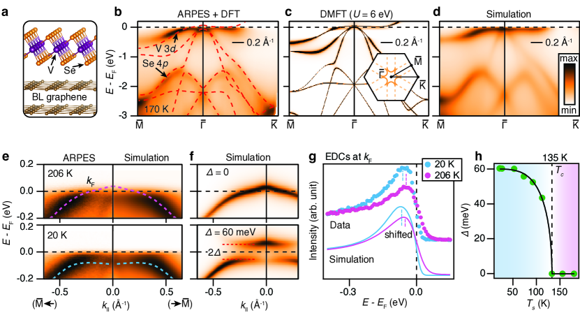
We apply TR-ARPES in order to investigate the microscopic origin of the insulator-metal transition in SL VSe2 grown on bilayer (BL) graphene Duvjir et al. (2018); Feng et al. (2018). Before discussing the results of pump-probe experiments, we start by clarifying the electronic structure of the material and characterize the phase transition in static conditions. Above the critical temperature , the material assumes the 1T structural modification where the V and Se atoms are coordinated in an octahedral geometry as shown in Fig. 1(a). The dispersion of this phase is calculated using density functional theory (DFT) and presented together with an ARPES spectrum along the high symmetry -- direction in Fig. 1(b). The shallow states around are composed of V 3 orbitals while the dispersive subbands at higher binding energies derive from Se 4 orbitals (see Supplementary Fig. S1). The increased broadening of V 3 states with energy below and the enhanced effective masses compared to the DFT dispersion are the telltale signs of correlation effects. Indeed, we find that these effects are captured in our dynamical mean-field theory (DMFT) calculations for a relatively large Hubbard interaction strength as shown in Fig. 1(c) for eV (see also Supplementary Fig. S2).
In order to deconvolve single-particle and many-body effects from the ARPES spectra we are following the phenomenological model of the photoemission intensity, Damascelli et al. (2003). Here, is the spectral function, incorporates the single-electron dipole matrix elements that govern the selection rules of the photoemission process and is the Fermi-Dirac (FD) distribution function with chemical potential and electronic temperature . By combining the bare dispersion obtained from DFT with the electronic self-energy, , deduced from the DFT and LDA + DMFT calculation, we are able to construct the spectral function of SL VSe2, as described in further details in the Methods. A numerical simulation of with self-energy and matrix elements adjusted to give an optimum description of the measured 2D image of the photoemission intensity is shown in Fig. 1(d), providing a basic model to interpret ARPES spectra of SL VSe2 in the following discussion.
We focus on measurements along the - high symmetry direction in order to track the opening of a gap in the Fermi surface segment shown in the Brillouin zone (BZ) sketch in Fig. 1(c), which occurs when the sample is cooled below Duvjir et al. (2018); Umemoto et al. (2019). A detailed view of this cut is presented for sample temperatures of 206 and 20 K around the Fermi crossing in Fig. 1(e). A significant -dependent change of the V 3 dispersion is seen via the purple and blue dashed curves that have been extracted using our 2D simulation of the intensity (see transition in Supplementary Video 1). The change of dispersion is linked to the gap opening described in terms of the parameter , which is demonstrated in the simulation with the FD function removed in Fig. 1(f). For the band crosses , however, the intensity around the band maximum is not seen in the ARPES data because these states are unoccupied. As assumes a finite value, a gap of opens, leading to increased spectral weight around below . The presence of such a gap is further corroborated by a shift of the peak away from in energy distribution curve (EDC) cuts at as is lowered, which is demonstrated in Fig. 1(g). The complete -dependence of is determined by fitting the 2D ARPES intensity measured at several temperatures, leading to the phase diagram in Fig. 1(h). The critical temperature found using this method is K, which is consistent with previous studies Feng et al. (2018); Duvjir et al. (2018).
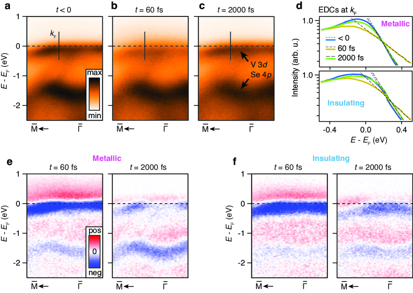
On the basis of the spectroscopic signatures and modeling of the insulator-metal transition specified above, we are now able to analyze the time-dependent response of SL VSe2 to an optical excitation. Measurements performed with sample temperatures of 200 K and 88 K are compared in order to track the dynamics in both the metallic and insulating phases. TR-ARPES snapshots are shown along - in Figs. 2(a)-(c) for excitation of the metallic phase using a pump pulse with an energy of 1.56 eV, temporal width of 30 fs and a fluence around 5 mJ/cm2 at a time delay before the optical excitation (), at the peak of the excitation ( fs) and at a longer delay ( fs). The excitation leads to a substantial decrease in intensity in the V 3 states around (see panel (b)), which does not fully recover at longer delays (see panel (c)). The raw -dependent intensity measured under the same conditions for the insulating phase appears similar on a superficial view (see Supplementary Fig. S3 for a comparison). A comparison of EDCs at , shown on a logarithmic intensity scale in Fig. 2(d), reveals exponential tails with a -dependent slope indicating the generation of hot carriers with an elevated electronic temperature in both phases.
A stronger indication for the spectral changes following excitation is obtained by calculating the difference in photoemission intensity by subtracting a spectrum determined in equilibrium conditions before the arrival of the pump pulse from the spectrum measured at a given delay time as shown for the two phases in Figs. 2(e)-(f) and Supplementary Video 2. A highly complex - and -dependence of intensity depletion and increase is seen. Surprisingly, we observe strong difference signals persisting at long delays ( fs) that look dramatically different for the two phases. Naively, one could think of assigning these changes to the mere redistribution of charge carriers in the V 3 and Se 4 states with excited holes (electrons) signified by the blue (red) regions of the spectra. However, the intensity is simultaneously affected by a change of the FD distribution due to the elevated electronic temperature , a -dependence of the quasiparticle scattering rate that manifests itself as increased broadening of the bands Andreatta et al. (2019); Ulstrup et al. (2015a), and the possibility of a -dependent in the insulating phase. Using our model of the photoemission intensity presented in Fig. 1(d) we fit , and such that our simulated intensity gives an optimum description of the ARPES intensity at all measured time delays, noting that for the metallic phase (see Methods and Supplementary Section 3 for further details of the fit). An excellent fit is obtained for all time delays in both phases using our assumption of a hot carrier model where the simulated intensity always incorporates a well-defined FD function, indicating that thermalization occurs via electron-electron interactions on a faster timescale than we can resolve ( fs) Johannsen et al. (2013).
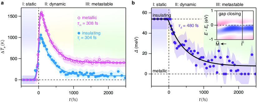
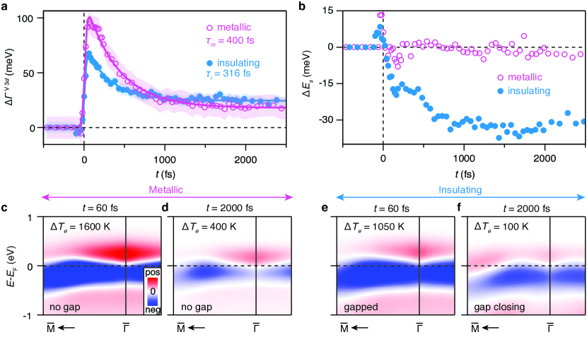
The change of electronic temperature extracted from this analysis is presented in Fig. 3(a), revealing a qualitatively similar -dependence in the two phases that can be divided according to (I) a static period before excitation, (II) a dynamic period with a sharp rise of during excitation followed by an initial fast relaxation and (III) a metastable period where the system remains out of equilibrium and does not relax on the timescale of our measurement. The transient increase in electronic temperature is caused by ultrafast energy transfer from the laser pulse to the electrons in the V 3 states. Energy is then transferred from electrons to the lattice leading to a decay of on a timescale of 300 fs. Both insulating and metallic phases subsequently reach a stable elevated electronic temperature compared to equilibrium, indicating that electron and lattice subsystems have reached a thermal equilibrium with a temperature larger than .
Figure 3(b) presents the extracted -dependence of from the TR-ARPES measurement of the insulating phase, revealing a transient closure of the gap during the dynamic period (region II), leaving the system in a metastable metallic phase (region III). The intensity difference between the fitted spectrum in this metastable metallic state and the insulating state in equilibrium (region I) essentially reproduces the measured behavior, as seen by comparing the inset in Fig. 3(b) with the difference spectrum at fs in Fig. 2(f) (see Supplementary Fig. S5 for other fit parameters and fitted difference spectra in the metallic phase). Note that this distinct redistribution of intensity is highly reproducible over multiple samples as shown in Supplementary Fig. S6 and the change in is essential for its simulation. The timescale where goes to zero is comparable to the time it takes the electronic system to transfer energy to the lattice as seen in region II in Fig. 3(a). As the lattice is thermally excited it obtains sufficient energy to rearrange atoms and trigger the insulator-metal transition, which is clocked to the time constant fs obtained from an exponential fit. This is on the order of quenching times observed for strong electron-lattice coupling CDWs in bulk TMDCs and significantly slower than the timescales associated with melting of Mott gaps driven by electron-electron interactions Sohrt et al. (2014).
The appearance of a metastable state is strongly indicative of a slow reconfiguration of the thermally excited lattice, possibly involving the distorted () and () superstructures found in the insulating phase of SL VSe2 Feng et al. (2018); Duvjir et al. (2018); Chen et al. (2018); Wong et al. (2019). This situation bears a striking resemblance to VO2 where an ultrafast excitation transforms an insulating phase with a monoclinic structure to a metallic phase with a rutile structure Cavalleri et al. (2001, 2004); Kübler et al. (2007). Such dynamics in SL VSe2 may be resolved in future studies utilizing ultrafast probes of the lattice structure.
In conclusion, we have tracked the spectral function of SL VSe2 across an ultrafast insulator-metal transition triggered by an intense optical excitation. The spectroscopic signatures of hot carrier dynamics and phase transition could be disentangled, revealing that electron-lattice energy exchange drives the transition in the first few hundreds of femtoseconds following excitation and leads to a metastable metallic state. Such a situation is not only intriguing for the application of 2D materials in electronic memory devices, but the coupling between electron and lattice degrees of freedom is also of fundamental interest for understanding the interplay of CDW physics and magnetism in 2D.
I Acknowledgement
We thank Phil Rice, Alistair Cox and David Rose for technical support during the Artemis beamtime. We gratefully acknowledge funding from VILLUM FONDEN through the Young Investigator Program (Grant. No. 15375) and the Centre of Excellence for Dirac Materials (Grant. No. 11744), the Danish Council for Independent Research, Natural Sciences under the Sapere Aude program (Grant Nos. DFF-9064-00057B and DFF-6108-00409) and the Aarhus University Research Foundation. This work is also supported by National Research Foundation (NRF) grants funded by the Korean government (nos. NRF-2020R1A2C200373211 and 2019K1A3A7A09033389) and by the International Max Planck Research School for Chemistry and Physics of Quantum Materials (IMPRS-CPQM). The authors also acknowledge The Royal Society and The Leverhulme Trust. Access to the Artemis Facility was funded by STFC. The Advanced Light Source is supported by the Director, Office of Science, Office of Basic Energy Sciences, of the U.S. Department of Energy under Contract No. DE-AC02-05CH11231.
II Competing Interests
The authors declare that they have no competing financial interests.
III Additional information
Supplementary Information and two Supplementary Videos accompany this paper.
Correspondence and requests for materials should be addressed to S. U. (ulstrup@phys.au.dk).
IV Methods
Sample preparation. SL VSe2 samples were grown on BL graphene on 6H-SiC(0001) using molecular beam epitaxy (MBE) with a base pressures better than Torr. The sample measured to produce the data in Fig. 1(b) was grown at the University of St Andrews, UK. The remaining spectra were collected on samples grown at the University of Seoul, Republic of Korea. To obtain the BL graphene on SiC, the SiC substrates were outgassed at 650 ∘C for a few hours and then annealed three times up to 1300 ∘C for 2 min. The formation of BL graphene was verified by reflection high-energy electron diffraction (RHEED) and low-energy electron diffraction (LEED). High-purity V (99.8%) and Se (99.999%) were simultaneously evaporated while the substrate was kept at 250 ∘C. The growth process was monitored with in situ RHEED. The growth rate was fixed at 5 min per Se-V-Se layer. After growth, the sample was annealed at 450 ∘C for 30 min. A 100 nm Se film was deposited at room temperature to protect the sample while transferring through air. This Se capping layer was removed by annealing the sample at 300 ∘C for several hours in the UHV analysis chamber before photoemission experiments. No noticeable change in sample quality was observed due to the capping and de-capping procedure.
Static ARPES experiments. The ARPES spectrum shown in Fig. 1(b) was collected using a high-intensity He lamp ( = 21.2 eV, p-polarization) and a SPECS Phoibos 225 hemispherical electron analyzer at University of St Andrews, UK. Here, samples were directly transferred from the attached MBE growth chamber to the ARPES chamber. The remaining static measurements were performed in the microARPES end-station (base pressure of 3 Torr) at the MAESTRO facility at beamline 7.0.2 of the Advanced Light Source, Lawrence Berkeley National Laboratory. The ARPES system was equipped with a Scienta R4000 electron analyzer. We used a photon energy of 48 eV for -dependent scans. The total energy and angular resolution of our experiments were better than 20 meV and , respectively.
TR-ARPES experiments. The Materials Science end station of the Artemis facility at Rutherford Appleton Laboratory was used for TR-ARPES measurements. Synchronized infrared (IR) pump and extreme ultraviolet (EUV) probe beams were generated from a Ti:Sapphire laser system at 12 mJ, 1 kHz, with a 30 fs pulse length and a central wavelength of 795 nm. The output of the laser was split: a small fraction of the energy was used directly to pump the sample at 1.56 eV, with fine control of the fluence achieved using a half waveplate and a thin film polariser, while 2 mJ pulse energy was used to prepare the probe beam by high-harmonic generation. The laser was focused into a thin Ar gas cell to generate a comb of odd harmonics in the EUV. The 19th harmonic at 29.6 eV was selected, using a time-preserving monochromator Frassetto et al. (2011). The two beam polarisations were orthogonal: the pump beam was s-polarised while the probe beam was p-polarised. The end station is equipped with a SPECS Phoibos 100 hemispherical electron energy analyser. Experiments were performed in the wide-angle mode, with a slit size of 1 mm. The time and angular resolution of the experiments were 46 fs and 0.3∘, respectively. The optimum energy resolution was 250 meV, as determined through our simulations of the photoemission intensity. Energy resolution is limited by analyzer energy resolution (about 190 meV), EUV probe pulse broadening (about 100 meV), and space charge effects (about 130 meV). Temperatures from 88 to 220 K were reached using an open-cycle liquid He cryostat.
Theory. The LDA+DMFT calculations were performed at a temperature of K, assuming a Hund’s rule coupling eV and scanning different values of the screened Hubbard interaction strength from 5 to 9 eV. We utilized the DMFT package for the electronic structure calculations of Ref. Haule et al. (2010) interfaced with the local density approximation (LDA) functional implemented in Wien2k Blaha et al. (2001) and we adopted the fully-localized-limit scheme for the double-counting functional Anisimov et al. (1997). All simulations have been performed with 10000 -points and and employing the continuous-time quantum Monte-Carlo (CTQMC) impurity solver Gull et al. (2011); Werner et al. (2006); Haule (2007). The spectral properties were mapped onto the real axis using the maximum entropy method Jarrell and Gubernatis (1996). The DFT calculations were performed using a Perdew, Burke, and Ernzerhof (PBE) functional Perdew et al. (1996).
Simulation of ARPES intensity. The photoemission intensity is described by the expression as explained in the main text. The subscript is the band index. The spectral function is written as Damascelli et al. (2003); Nechaev et al. (2009); Andreatta et al. (2019),
| (1) |
where is the non-interacting band dispersion or bare band, which we describe using the DFT dispersion as an input. and are the real and imaginary parts of the electronic self energy , respectively. In our simulation the correlation effects in the V 3 states, including the gap opening of the dispersion, are included in through the expression (see Supplementary Section 1 for further details)
| (2) |
Here is a constant energy shift of the states, is the quasiparticle residue, is quasi-particle scattering rate, is the gap parameter and is a constant related to the change in the scattering rate due to the presence of a gap. We also used a parameter, labeled , to describe any rigid shift of all the bands including . Such a shift may arise due to an external electric field associated with vacuum space charge or surface photo voltage Ulstrup et al. (2015b). Finally, the ARPES intensity is obtained by convoluting the photoemission intensity by two Gaussians representing the energy () and momentum () resolution broadening of the instrument,
| (3) |
We expand in second order polynomial terms of both and Andreatta et al. (2019). The Se 4 states at higher binding energies are well-described by the DFT bands and using a scattering rate that is merely expressed in terms of first order polynomials of and . The parameters describing , and are found in static conditions by performing a 2D fit of the simulated intensity to the ARPES spectra. We find that a satisfactory fit is obtained using a quasiparticle residue in the range of 0.52 to 0.54. For the fits of the TR-ARPES data we account for the time dependent changes of FD distribution and spectral function by allowing a variation of , and the self-energy through the scattering rate () and the gap parameter . We allow for a slight adjustment of the energy- and momentum-position of the bands to ensure consistency between measured and fitted spectra. The resulting parameters of the fit to the TR-ARPES data are given in Fig. 3 and Supplementary Fig. S5.
IV.1 Supplementary Section 1: Form of the self energy in ARPES simulations
The following mathematical form of the self energy was utilized in our simulations for interpreting the ARPES data, within an energy window of 0.5 eV from the Fermi level:
| (4) |
Here is the momentum, is the energy, is a generic band eigenvalue, is scattering rate, is the gap parameter, is a constant related to the change in scattering rate due to and is the momentum-independent (local) component of the self-energy:
| (5) |
which we approximated assuming a linear structure characterized by the quasiparticle residue and a constant energy shift .
To explain the physical reasons underlying Eq. (4) we note that the corresponding momentum-resolved single-particle Green’s function is represented as follows:
| (6) |
where
| (7) |
In fact, the last expression in Eq. (6) has the same mathematical structure of the phenomenological self-energy previously used for fitting ARPES data in the presence of a superconducting or charge density wave (CDW) gap Norman et al. (1998); Chen et al. (2018). Therefore, in this work, Eq. (4) is designed to represent the CDW effects on a band structure consisting of pre-existing quasi-particle excitations renormalized by electron correlations.
| 5 eV | 0.50635 | 0.78723 | 0.80550 |
| 6 eV | 0.49489 | 0.75884 | 0.77807 |
| 7 eV | 0.47736 | 0.73362 | 0.75279 |
| 8 eV | 0.45801 | 0.70974 | 0.72878 |
| 9 eV | 0.43984 | 0.68810 | 0.70745 |
Note that in Eq. (5) we assumed that acts as a number rather than a matrix. However, in general, the self-energy correction shall be expected to be significant only for the V 3 degrees of freedom. Furthermore, considering the symmetry of our system, the , and components of the self-energy are not a-priori equal, as they belong to distinct irreducible representations of the point symmetry group of the V atoms. On the other hand, Eq. (5) is a meaningful approximation provided that, for energies within 0.5 eV around the Fermi level, the following hypothesis are verified:
-
1)
Most of the spectral weight arises from the V 3 electrons.
-
2)
The self-energy is approximately orbital-independent.
-
3)
The momentum-independent local component of the self-energy is approximately real and linear with respect to the frequency.
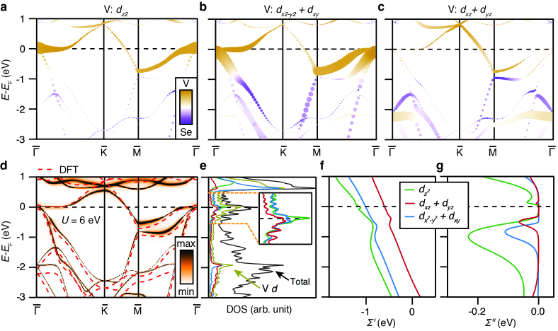
Here we use DFT and LDA+DMFT calculations to prove that these hypotheses are, in fact, approximately applicable to our system. We show the DFT calculated bands resolved with respect to their orbital character in Fig. 4(a)-(c). These calculations indicate that the bands have mostly V 3 character near the Fermi level. Specifically, the spectral weight is dominated by the , contributions. Fig. 4(d) illustrates the LDA+DMFT band structure obtained for a screened Hubbard interaction strength eV and a Hund’s coupling constant eV. The orbitally-resolved LDA+DMFT local DOS in Fig. 4(e) confirms that, consistent with DFT, most of the spectral weight near the Fermi level has V 3 character. Finally, as shown in Fig. 4(f) and (g), the self-energy is approximately linear and similar for all of the V 3 orbitals for energies eV with respect to the Fermi level. This observation is consistent with the LDA+DMFT quasi-particle weights:
| (14) |
see Table 1, which are all , in agreement with our simulation (in the range 0.52 to 0.54).

In Fig. 5 we show the LDA+DMFT bands for three different values of the Hubbard interaction strength . The bands are found to be very similar for these values. This indicates that our theoretical predictions are robust.
IV.2 Supplementary Section 2: Raw ARPES spectra in metallic and insulating phase
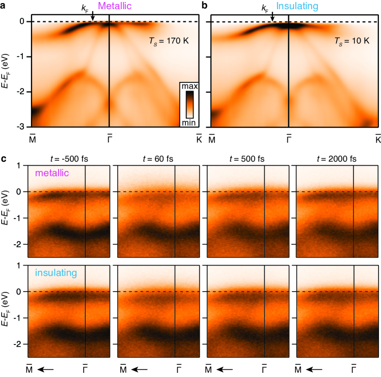
Fig. 6(a) and (b) show static ARPES spectra for both metallic and insulating phases. The dispersion of the top V 3 band is different close to due to the formation of the energy gap in the insulating phase. Figure 6(c) presents TR-ARPES snapshots of the spectral changes in these two scenarios before and after optical excitation.
IV.3 Supplementary Section 3: Simulation of ARPES spectra
As mentioned in the methods section of the main text, the ARPES intensity can be expressed as,
| (15) |
The energy and momentum resolution functions ( and ) are known from instrument calibration and remain fixed for a given measurement. Furthermore, in static ARPES measurements we use that and such that is fully specified. The parameters describing and are obtained by performing a 2D fit of a simulated -dependent intensity to the corresponding ARPES spectrum. Since the values of and at a given are intrinsic properties of the V states that are independent of measurement configuration, we apply the values obtained from the static ARPES simulations to describe the TR-ARPES spectra. The parameters describing are related to the photoemission setup, however, we use the assumption that is independent of time such that the matrix element is always determined in the equilibrium part of the TR-ARPES measurements. Data points acquired for fs are described using a single optimized spectrum, as the system is in equilibrium. The parameters of this optimized spectrum are used as input for the fit of the TR-ARPES data points acquired at the remaining time delay points.
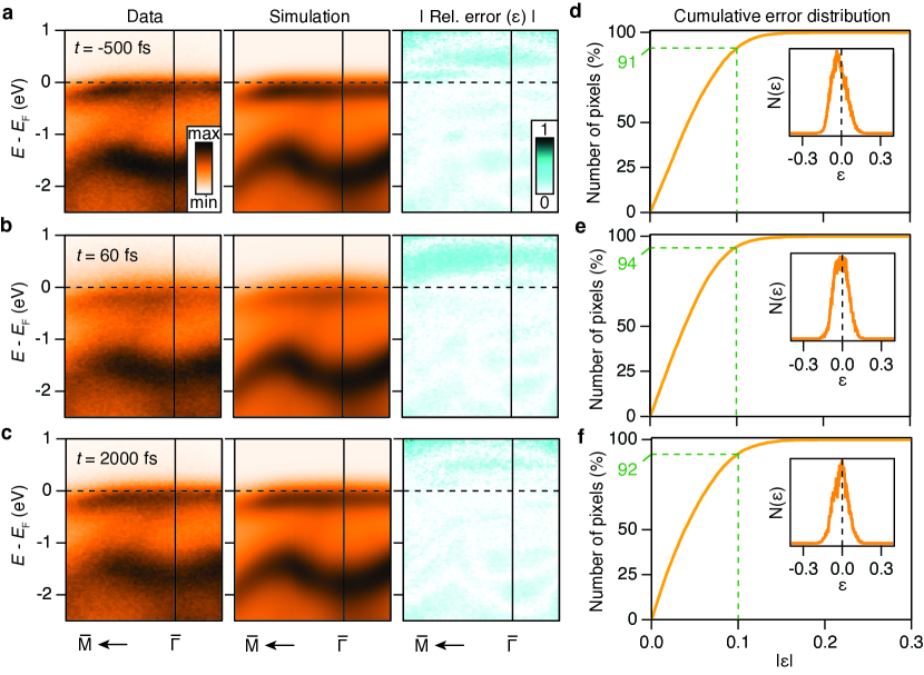
In Figs. 7(a)-(c) we show the TR-ARPES spectra, simulated spectra and the corresponding unsigned relative error () at fs, 60 fs and 2000 fs for the metallic phase ( K). The associated cumulative distribution of is given in Figs. 7(d)-(f). As the actual intensity for the pixels above is very small, irrespective of the simulation quality, the relative error for these pixels are high. We have therefore selected the energy range from -2.5 eV to for our error analysis. All fitted pixels that fall below a margin set by are deemed as providing a satisfactory agreement between model and data. We find that this is the case for 92% of the pixels for all the three time delays. The symmetric distribution of the relative error (see inserts in Figs. 7(d)-(f)) with respect to shows the unbiased nature of our simulation.
In Figs. 8(a) and (b) we show the changes in the remaining fit parameters - scattering rate () associated with the V 3 band and the energy shift () which accompany the parameters and shown in Fig. 3 of the main text. Figs. S5(c)-(f) present the intensity difference calculated by subtracting the fitted equilibrium spectra from the fitted spectra at fs and fs, which may be compared with the experimental results in Figs. 2(e) and (f) of the main manuscript.
IV.4 Supplementary Section 4: Reproducibility of intensity difference signals
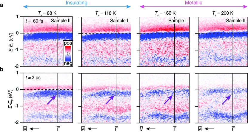
We have performed consistency checks of the observed intensity difference by repeating the measurements discussed in the main manuscript for sample temperatures of 88 K, 118 K, 166 K and 200 K and for two independent SL VSe2 samples, verifying that the spectral signatures are robust for the two phases across K. Figure 9 summarizes these results by presenting the corresponding intensity difference spectra.
References
- Xi et al. (2015) X. Xi, L. Zhao, Z. Wang, H. Berger, L. Forró, J. Shan, and K. Mak, Nat. Nanotechnol. 10, 765 (2015).
- Ugeda et al. (2016) M. Ugeda, A. Bradley, Y. Zhang, S. Onishi, Y. Chen, W. Ruan, O. Claudia, H. Ryu, M. Edmonds, H. Tsai, et al., Nat. Phys. 12, 92 (2016).
- Sanders et al. (2016) C. E. Sanders, M. Dendzik, A. S. Ngankeu, A. Eich, A. Bruix, M. Bianchi, J. A. Miwa, B. Hammer, A. A. Khajetoorians, and P. Hofmann, Phys. Rev. B 94, 081404 (2016).
- Pásztor et al. (2017) Á. Pásztor, A. Scarfato, C. Barreteau, E. Giannini, and C. Renner, 2D Mater. 4, 041005 (2017).
- Chen et al. (2020) Y. Chen, W. Ruan, M. Wu, S. Tang, H. Ryu, H.-Z. Tsai, R. Lee, S. Kahn, F. Liou, C. Jia, et al., Nat. Phys. 16, 218 (2020).
- Duvjir et al. (2018) G. Duvjir, B. K. Choi, I. Jang, S. Ulstrup, S. Kang, T. Thi Ly, S. Kim, Y. H. Choi, C. Jozwiak, A. Bostwick, et al., Nano Lett. 18, 5432 (2018).
- Feng et al. (2018) J. Feng, D. Biswas, A. Rajan, M. D. Watson, F. Mazzola, O. J. Clark, K. Underwood, I. Marković, M. McLaren, A. Hunter, et al., Nano Lett. 18, 4493 (2018).
- Chen et al. (2018) P. Chen, W. W. Pai, Y.-H. Chan, V. Madhavan, M. Y. Chou, S.-K. Mo, A.-V. Fedorov, and T.-C. Chiang, Phys. Rev. Lett. 121, 196402 (2018).
- Strocov et al. (2012) V. N. Strocov, M. Shi, M. Kobayashi, C. Monney, X. Wang, J. Krempasky, T. Schmitt, L. Patthey, H. Berger, and P. Blaha, Phys. Rev. Lett. 109, 086401 (2012).
- Umemoto et al. (2019) Y. Umemoto, K. Sugawara, Y. Nakata, T. Takahashi, and T. Sato, Nano Res. 12, 165 (2019).
- Bonilla et al. (2018) M. Bonilla, S. Kolekar, Y. Ma, H. C. Diaz, V. Kalappattil, R. Das, T. Eggers, H. R. Gutierrez, M.-H. Phan, and M. Batzill, Nat. Nanotechnol. 13, 289 (2018).
- Coelho et al. (2019) P. M. Coelho, K. Nguyen Cong, M. Bonilla, S. Kolekar, M.-H. Phan, J. Avila, M. C. Asensio, I. I. Oleynik, and M. Batzill, J. Phys. Chem. C 123, 14089 (2019).
- Wong et al. (2019) P. K. J. Wong, W. Zhang, F. Bussolotti, X. Yin, T. S. Herng, L. Zhang, Y. L. Huang, G. Vinai, S. Krishnamurthi, D. W. Bukhvalov, et al., Adv. Mater. 31, 1901185 (2019).
- Cavalleri et al. (2001) A. Cavalleri, C. Tóth, C. W. Siders, J. A. Squier, F. Ráksi, P. Forget, and J. C. Kieffer, Phys. Rev. Lett. 87, 237401 (2001).
- Perfetti et al. (2006) L. Perfetti, P. A. Loukakos, M. Lisowski, U. Bovensiepen, H. Berger, S. Biermann, P. S. Cornaglia, A. Georges, and M. Wolf, Phys. Rev. Lett. 97, 067402 (2006).
- Hellmann et al. (2012) S. Hellmann, T. Rohwer, M. Kalläne, K. Hanff, C. Sohrt, A. Stange, A. Carr, M. M. Murnane, H. C. Kapteyn, L. Kipp, et al., Nat. Commun. 3, 1069 EP (2012).
- Rohwer et al. (2011) T. Rohwer, S. Hellmann, M. Wiesenmayer, C. Sohrt, A. Stange, B. Slomski, A. Carr, Y. Liu, L. M. Avila, M. Kallane, et al., Nature 471, 490 (2011).
- Petersen et al. (2011) J. C. Petersen, S. Kaiser, N. Dean, A. Simoncig, H. Y. Liu, A. L. Cavalieri, C. Cacho, I. C. E. Turcu, E. Springate, F. Frassetto, et al., Phys. Rev. Lett. 107, 177402 (2011).
- Mathias et al. (2016) S. Mathias, S. Eich, J. Urbancic, S. Michael, A. V. Carr, S. Emmerich, A. Stange, T. Popmintchev, T. Rohwer, M. Wiesenmayer, et al., Nat. Commun. 7, 12902 EP (2016).
- Graf et al. (2011) J. Graf, C. Jozwiak, C. L. Smallwood, H. Eisaki, R. A. Kaindl, D.-H. Lee, and A. Lanzara, Nat. Phys. 7, 805 EP (2011).
- Smallwood et al. (2012) C. L. Smallwood, J. P. Hinton, C. Jozwiak, W. Zhang, J. D. Koralek, H. Eisaki, D.-H. Lee, J. Orenstein, and A. Lanzara, Science 336, 1137 (2012).
- Sohrt et al. (2014) C. Sohrt, A. Stange, M. Bauer, and K. Rossnagel, Faraday Discuss. 171, 243 (2014).
- Perfetti et al. (2007) L. Perfetti, P. A. Loukakos, M. Lisowski, U. Bovensiepen, H. Eisaki, and M. Wolf, Phys. Rev. Lett. 99, 197001 (2007).
- Monney et al. (2016) C. Monney, M. Puppin, C. W. Nicholson, M. Hoesch, R. T. Chapman, E. Springate, H. Berger, A. Magrez, C. Cacho, R. Ernstorfer, et al., Phys. Rev. B 94, 165165 (2016).
- Damascelli et al. (2003) A. Damascelli, Z. Hussain, and Z.-X. Shen, Rev. Mod. Phys. 75, 473 (2003).
- Andreatta et al. (2019) F. Andreatta, H. Rostami, A. G. Čabo, M. Bianchi, C. E. Sanders, D. Biswas, C. Cacho, A. J. H. Jones, R. T. Chapman, E. Springate, et al., Phys. Rev. B 99, 165421 (2019).
- Ulstrup et al. (2015a) S. Ulstrup, J. C. Johannsen, A. Crepaldi, F. Cilento, M. Zacchigna, C. Cacho, R. T. Chapman, E. Springate, F. Fromm, C. Raidel, et al., J. Phys.: Condens. Matter 27, 164206 (2015a).
- Johannsen et al. (2013) J. C. Johannsen, S. Ulstrup, F. Cilento, A. Crepaldi, M. Zacchigna, C. Cacho, I. C. E. Turcu, E. Springate, F. Fromm, C. Raidel, et al., Phys. Rev. Lett. 111, 027403 (2013).
- Cavalleri et al. (2004) A. Cavalleri, T. Dekorsy, H. H. W. Chong, J. C. Kieffer, and R. W. Schoenlein, Phys. Rev. B 70, 161102 (2004).
- Kübler et al. (2007) C. Kübler, H. Ehrke, R. Huber, R. Lopez, A. Halabica, R. F. Haglund, and A. Leitenstorfer, Phys. Rev. Lett. 99, 116401 (2007).
- Frassetto et al. (2011) F. Frassetto, C. Cacho, C. A. Froud, I. E. Turcu, P. Villoresi, W. A. Bryan, E. Springate, and L. Poletto, Opt. Express 19, 19169 (2011).
- Haule et al. (2010) K. Haule, C.-H. Yee, and K. Kim, Phys. Rev. B 81, 195107 (2010).
- Blaha et al. (2001) P. Blaha, K. Schwarz, G. K. Madsen, D. Kvasnicka, and J. Luitz, An augmented plane wave+ local orbitals program for calculating crystal properties (2001).
- Anisimov et al. (1997) V. I. Anisimov, F. Aryasetiawan, and A. I. Lichtenstein, J. Phys.: Condens. Matter 9, 767 (1997).
- Gull et al. (2011) E. Gull, A. J. Millis, A. I. Lichtenstein, A. N. Rubtsov, M. Troyer, and P. Werner, Rev. Mod. Phys. 83, 349 (2011).
- Werner et al. (2006) P. Werner, A. Comanac, L. de’ Medici, M. Troyer, and A. J. Millis, Phys. Rev. Lett. 97, 076405 (2006).
- Haule (2007) K. Haule, Phys. Rev. B 75, 155113 (2007).
- Jarrell and Gubernatis (1996) M. Jarrell and J. Gubernatis, Phys. Rep. 269, 133 (1996).
- Perdew et al. (1996) J. P. Perdew, K. Burke, and M. Ernzerhof, Phys. Rev. Lett. 77, 3865 (1996).
- Nechaev et al. (2009) I. A. Nechaev, M. F. Jensen, E. D. L. Rienks, V. M. Silkin, P. M. Echenique, E. V. Chulkov, and P. Hofmann, Phys. Rev. B 80, 113402 (2009).
- Ulstrup et al. (2015b) S. Ulstrup, J. C. Johannsen, F. Cilento, A. Crepaldi, J. A. Miwa, M. Zacchigna, C. Cacho, R. T. Chapman, E. Springate, F. Fromm, et al., J. Electron Spectrosc. Relat. Phenom. 200, 340 (2015b).
- Norman et al. (1998) M. Norman, M. Randeria, H. Ding, and J. Campuzano, Phys. Rev. B 57, R11093 (1998).