Transmission phase read-out of a large quantum dot in a nanowire interferometer
Abstract
Detecting the transmission phase of a quantum dot via interferometry can reveal the symmetry of the orbitals and details of electron transport. Crucially, interferometry will enable the read-out of topological qubits based on one-dimensional nanowires. However, measuring the transmission phase of a quantum dot in a nanowire has not yet been established. Here, we exploit recent breakthroughs in the growth of one-dimensional networks and demonstrate interferometric read-out in a nanowire-based architecture. In our two-path interferometer, we define a quantum dot in one branch and use the other path as a reference arm. We observe Fano resonances stemming from the interference between electrons that travel through the reference arm and undergo resonant tunnelling in the quantum dot. Between consecutive Fano peaks, the transmission phase exhibits phase lapses that are affected by the presence of multiple trajectories in the interferometer. These results provide critical insights for the design of future topological qubits.
I Introduction
Similar to a light wave, an electron wave acquires a phase when interacting with a scattering centre. Studying this effect requires an interferometer with phase-coherent transport such as semiconducting or metallic rings WEB1985; BAC1999; RUS2008. In these nanostructures, the phase difference between the two paths () can be tuned by a magnetic flux via the Aharonov-Bohm (AB) effect:
| (1) |
with the magnetic flux through the interferometer and the flux quantum.
When the scattering centre is a quantum dot (QD), as depicted in Fig. 1a, the transmission phase provides information complementary to the transmission probability , with the transmission amplitude . It can reveal insights into microscopic details of electron transport and into the spatial symmetries of the orbitals LEE1998; ORE2007; SIL200; VAN2006.
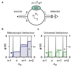
Recently, theoretical proposals suggested using interferometry as a read-out method of topological qubits, where quantum information is encoded in the electron parity of Majorana modes in semiconducting-superconducting nanowires KIT2001; LUT2010; ORE2010; ALI2012; VIJ2016; PLU2017; KAR2017. Here, opposite qubit states are characterised by different transmission phases similar to the mesoscopic phase behaviour observed in few-electron quantum dots (Fig. 1b) FU2010; DRU2018; HEL2018; AVI2005.
When Majorana modes are absent, the phase is expected to exhibit the universal behaviour detected in many-electron quantum dots. In these systems, abrupt phase lapses break the simple parity-to-phase relation (Fig. 1c) YAC1995; SCH1997; ORE2007; KAR2007; AVI2005; EDL2017.
Despite the critical application in topological qubits, the phase read-out of a quantum dot in a nanowire interferometer has not been demonstrated yet.
While pioneering works employed two-dimensional electron gases YAC1995; SCH1997; AVI2005; EDL2017, here we take advantage of the recent advances in the growth of nanowire networks CAR2014; GAZ2017 and demonstrate interferometric read-out of a quantum dot defined in a nanowire. Our findings provide crucial insights for future topological qubits based on hybrid one-dimensional nanowire systems.
II Results
II.1 Cotunnelling Aharonov-Bohm interference
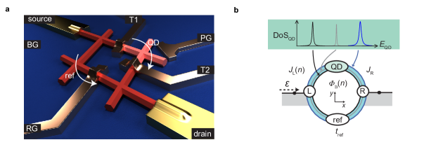
Our device is shown in Fig. 2a and consists of a hashtag-shaped network of hexagonal InSb nanowires of high crystalline quality GAZ2017. In the top-right arm, negative voltages ( and ) on the top gates, T1 and T2, create two tunnel barriers that define an X-shaped quantum dot (pink region). The voltage on the plunger gate PG () tunes its electron occupation. Likewise, the transmission in the bottom-left branch – the reference arm – can be varied from pinch-off to the open regime by adjusting the voltage on the reference gate (RG). The -doped-Si/SiOx substrate allows global back-gate (BG) functionality. A DC bias voltage with a small AC excitation, , is applied between source and drain, yielding a current . Both the DC current and the differential conductance are measured in a dilution refrigerator with an electron temperature of mK at its base temperature.
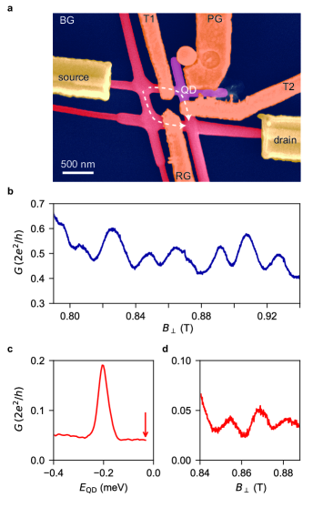
When the QD is not defined, the conductance at zero bias voltage displays Aharonov-Bohm oscillations as a function of the magnetic field perpendicular to the substrate () with period mT (Fig. 2b). This periodicity corresponds to a loop area of , which is consistent with the actual area of the device of measured up to the centre of the nanowires.
When the quantum dot is defined, we adjust the plunger-gate voltage between two resonances, as indicated by the red arrow in Fig. 2c, where the horizontal axis is the QD electrochemical potential (, with the lever arm and the electron charge). In this regime, the electron-electron repulsion in the dot suppresses the current almost completely, which is known as Coulomb blockade. Transport is then allowed only via virtual, higher-order processes. At zero bias, elastic cotunnelling is predominant and its phase coherence is critical for parity-protected read-out schemes of Majorana wires PLU2017; KAR2017.
When we balance the current distribution in the two arms of our device, the AB oscillations in the cotunnelling regime become visible with an amplitude of of the average conductance (Fig. 2d). The large visibility demonstrates that cotunnelling across the large Coulomb-blockaded dot is phase-coherent, fulfilling a fundamental requirement of future parity read-out circuits.
II.2 From Coulomb to Fano resonances
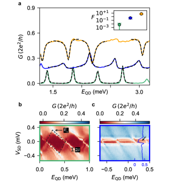
In order to characterize the quantum dot, we first pinch off the reference arm. The green trace in Fig. 3a displays a series of nearly equally spaced conductance peaks stemming from tunnelling via the dot. Their separation is also known as the addition energy and arises from two effects: the quantum confinement and the Coulomb interaction KOU2001. In a large dot, the second effect dominates over the first, leading to a series of peaks that are equidistant KOU2001; IHN2010. From the bias spectroscopy in Fig. 3b, we estimate the Coulomb charging energy meV (with the overall capacitance) and the level spacing due to confinement meV. We evaluate the first parameter from the size of the diamonds in bias voltage, and the second from the separation between the lines that confine the Coulomb diamonds and the lines that are due to the excited states. The large ratio of indeed arises from the large size of the dot, which is designed to be comparable with the typical micron-long semiconducting-superconducting dots of near-future explorations ALB2016; VAN2018; SHE2018. Assuming a typical open-channel electron density of PLI2013 and the dot volume of , we estimate the maximum number of electrons on the QD to be .
We now start to activate transport in the reference arm.
Upon increasing its transparency, the Coulomb peaks first evolve into the asymmetric peaks of the blue trace and then into the dips in the orange one of Fig. 3a.
The variation of their line-shapes stems from the Fano effect, a phenomenon observed in multiple contexts in physics: from Raman scattering CER1973; GUP2003 to photon absorption in quantum-well structures FAI1997; SCHM1997, from transport in single-electron transistors GOR2000 to Aharonov-Bohm interferometers KOB2002; AHA2006; HUA2015; RYU1998; KOB2003; KAT2004.
The effect originates from the interference between two partial waves: one is undergoing a resonant scattering and the other is travelling through a continuum of states. In our experiment, the first is mediated by the discrete dot spectrum provided by Coulomb blockade and confinement, and the second by the continuum of the density of states in the reference path. Bias spectroscopy with the reference path being partially conducting – similarly to the blue trace in Fig. 3a – shows Fano peaks extending into the Coulomb valleys at mV (cf. black arrows in Fig. 3c). To the best of our knowledge, this is the first observation of Fano physics in a nanowire-based interferometer.
To distinguish the three regimes of Fig. 3a, we fit the line-shapes of the peaks using a generalized Fano model AHA2006. The relevant ingredients are the coupling terms between the dot and the two leads ( and ), the transmission through the reference arm () and the magnetic flux through the ring (). A schematic illustration and more information are shown in the Methods and the result of the fits are listed in Supplementary Tables 1-3.
We extract the Fano parameter from each peak (or dip). The inset of Fig. 3a shows that the averages of across each trace extend over three orders of magnitude, reflecting the large tunability of the device.
II.3 The universal phase behaviour
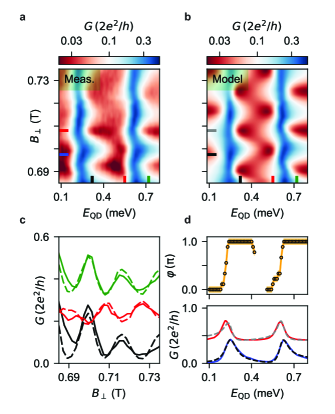
Upon sweeping the magnetic field, the Fano line-shapes vary periodically owing to the Aharonov-Bohm effect. In particular, Fig. 4a shows that two adjacent Fano resonances evolve in-phase.
We use the model described above to fit both peaks as a function of magnetic field, and we illustrate the result in Fig. 4b. The model captures well the main features of the experimental data, and the good agreement is visible in the line-cuts presented in Fig. 4c. Here, the three traces are taken at the positions denoted by the black, red, and green lines in both panels a and b.
A -shift in the AB oscillations is visible between both the black and red as well as the red and green traces. The complete evolution of the phase as a function of is extracted by tracking the maximum of the AB pattern and shown in the top panel of Fig. 4d. In the bottom panel, we present horizontal line-cuts of Figs. 4a and 4b at the positions indicated by the coloured lines.
Here, we observe two main features: a phase variation of at the resonances over an energy scale similar to the broadening of the peaks, and a phase lapse in the Coulomb valley. These are distinctive features of the universal phase behaviour and are consistent with the in-phase evolution of the two adjacent CPs in Fig. 4a YAC1995; SCH1997; ORE2007; KAR2007; AVI2005. The observation of the universal rather than the mesoscopic behaviour can be explained by taking a look at the energy scales of the transport. In our measurement, the typical dot coupling energy (meV) is a few times larger than the level spacing in the dot (meV). Therefore, tunnelling occurs via multiple dot-levels, a condition for which theory predicts the observation of the universal behaviour KAR2007; ORE2007.
Because previous experiments focused on the single-level regime () SCH1997; YAC1995; AVI2005 and in the crossover () EDL2017, finding both phase lapses and phase plateaus, our investigation in the fully multi-level regime () seems to complete the complex dot-interferometry puzzle.
II.4 Multi-path transport effects
In the following, we highlight that an optimal read-out of the transmission phase requires an interferometer close to the one-dimensional limit in the sense that it shoud comprise thin nanowires enclosing a relatively large hole.
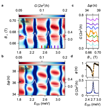
For a gate configuration different from the previous regime, the transmission phase varies smoothly between several pairs of adjacent CPs. Here, the phase displays a behaviour in between the universal and the mesoscopic regimes (Fig. 5a).
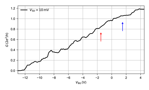
The two configurations differ in the back-gate voltage that has been lowered from V in Fig. 4 to V in Fig. 5.
Voltages on the tunnel gates are also re-adjusted to retain a similar transmission, whereas the plunger gate remains at . We estimate a reduction of the electron density by no more than compared to the first case, leaving the dot still in the many-electron regime (see Supplementary Figure 2).
In Fig. 5a, we show a color map of vs. and , exhibiting the evolution of 4 CPs. The red features in the cotunnelling regions oscillate as a function of owing to the AB effect. Several vertical line-cuts are shown in Fig. 5c. The maxima of the AB oscillations around T are converted into transmission phase via the magnetic field period (here mT) and displayed in the top panel of Fig. 5d. In the bottom panel of Fig. 5d, we show a horizontal line-cut taken at the position indicated by the blue line in Fig. 5a. Similar to the data in Fig. 4, the phase exhibits a variation concomitant with the peak in the conductance.
However, the phase lapse in the Coulomb valley is replaced by a smooth evolution. This slow phase variation is not universal, but depends on the specific gate setting.
We interpret this anomaly as a consequence of the relatively large width of the nanowires (nm). Microscopically, we speculate that consecutive charge states might not couple to the same loop trajectory. The presence of at least two paths gives rise to beatings in the magneto-conductance that conceal the evolution of the transmission phase AHA2006. Our interpretation is well-supported by the large width of the Aharonov-Bohm peak in the Fourier spectrum shown in Supplementary Figure 3.
While in reality multiple trajectories could couple to each QD orbital, we reproduce our observation in the model by linking each resonance to a possibly different AB periodicity. This simple assumption enables to capture the main features of the measurement (Fig. 5b).
The coexistence of the two distinct phase behaviours (Fig. 4 vs. Fig. 5) in the same mesoscopic device is hard to fully explain, and might be correlated with the exact coupling mechanism between the dot orbitals and the leads.
III Discussion
In summary, we report interferometric measurements on a quantum dot embedded in a network of four conjoint InSb nanowires. The observation of pronounced quantum interference in the cotunnelling regime and the presence of Fano resonances suggest that interferometry is a viable tool for parity read-out of future topological qubits in nanowire networks. Theory suggests that the transmission probability of a semiconducting-superconducting quantum dot in the topological regime should exhibit phase plateaus FU2010; DRU2018. However, transmitting channels other than the teleportation via Majorana bound states were not taken into account. In experiments, extended topologically trivial modes without an underlying topological bulk phase can mimic Majoranas. Hence, quasiparticle transport via these modes might offer parallel paths to the Majorana teleportation WHI2019; PRA2019. Altogether, these can cause phase lapses that hinder the simple correspondence between the transmission phase and the electron parity. We conclude by remarking that future interferometers for parity-state discrimination via phase read-out should be designed with a large ratio between circumference and nanowire diameter.
IV Methods
Device fabrication:
InSb networks are grown by combining the bottom-up synthesis of four monocrystalline nanowires and the accurate positioning of the nanowire seeds along trenches on an InP substrate. Further details on the nanowire growth are presented in refs. CAR2014 and GAZ2017.
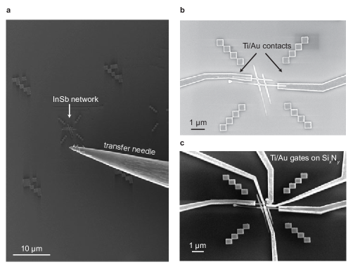
After the growth, we transfer nanowire networks from the InP growth chip onto a -doped Si/SiOx substrate (oxide thickness of nm) using a mechanical nanomanipulator installed in a scanning electron microscope. Ti/Au contact leads are patterned using electron-beam lithography and e-gun evaporation, following surface treatment of the InSb for minutes in a sulfur-rich ammonium polysulfide solution diluted in water () at C. The devices are covered with nm of sputtered SixNy acting as a gate dielectric. The second layer of Ti/Au electrodes is patterned and evaporated to define the top gates. The chip is then diced, mounted and bonded onto a commercial printed circuit board.
Transport measurements:
The device is cooled down in a dry dilution refrigerator equipped with a --T vector magnet. The base electron temperature is mK. Conductance across the device is measured via a standard low-frequency lock-in technique at an AC signal amplitude of V. The data presented in the main text and in Supplementary Figures 2, 3, and 4 are taken from a single device. In Supplementary Figures 5 and 6, we present data taken from a second and third device, respectively. The AC conductance in Figs. 2, 3, 4, and Supplementary Figure 4 was corrected for a constant offset that was later identified to arise from the setup.
Model of the Aharonov-Bohm interferometer:
The Landauer formula () connects the single-channel conductance of the system with the transmission probability . In Fig. 6, we show a schematic of the multi-path Aharonov-Bohm interferometer (a simple generalization of the single-path counterpart) next to an illustration of the actual device. The QD electrochemical potential ladder is represented as a series of discrete states, separated by the charging energy IHN2010. For the single-path case, hopping terms and couple the source (L) and drain (R) to the QD, respectively, with the Aharonov-Bohm phase included in , and and being real parameters. is the magnetic flux through the loop. When multiple-path are considered, we define the phase of as , with the parameter distinct for every CP.
The reference site has a slowly varying spectrum that we will assume for simplicity to be constant. The leads are assumed to be one-dimensional (lattice constant ) with hopping matrix elements and a typical energy dispersion of . The resulting transmission probability through the AB interferometer is AHA2006:
| (2) |
with
| (3) |
where represent the positions of the levels relevant in the tunnelling process on the -axis. For the fit of our results, we add an offset to eq. (2) to capture the incoherent contribution of the current through the device.
V Data availability
The data that support the findings of this study are available at https://doi.org/10.4121/uuid:9e625b55-11cf-4de2-8b81-32b5bf04d53d.
References
- (1) Webb, R. A., Washburn, S., Umbach, C. P. & Laibowitz, R. B. Observation of h/e Aharonov-Bohm oscillations in normal-metal rings. Phys. Rev. Lett. 54, 2696–2699 (1985).
- (2) Bachtold, A. et al. Aharonov-Bohm oscillations in carbon nanotubes. Nature 397, 673–675 (1999).
- (3) Russo, S. et al. Observation of Aharonov-Bohm conductance oscillations in a graphene ring. Phys. Rev. B 77, 085413 (2008).
- (4) Lee, H.-W. Generic transmission zeros and in-phase resonances in time-reversal symmetric single channel transport. Phys. Rev. Lett. 82, 2358–2361 (1998).
- (5) Oreg, Y. Universal phase lapses in a noninteracting model. New J. Phys. 9, 122, https://doi.org/10.1088/1367-2630/9/5/122 (2007).
- (6) Silvestrov, P. G. & Imry, Y. Towards an explanation of the mesoscopic double-slit experiment: A new model for charging of a quantum dot. Phys. Rev. Lett. 85, 2565–2568 (2000).
- (7) van Dam, J. A., Nazarov, Y. V., Bakkers, E. P. A. M., De Franceschi, S. & Kouwenhoven, L. P. Supercurrent reversal in quantum dots. Nature 442, 667–670 (2006).
- (8) Kitaev, A. Y. Unpaired Majorana fermions in quantum wires. Phys.-Uspekhi 44, 131–136 (2001).
- (9) Lutchyn, R. M., Sau, J. D. & Das Sarma, S. Majorana fermions and a topological phase transition in semiconductor-superconductor heterostructures. Phys. Rev. Lett. 105, 077001 (2010).
- (10) Oreg, Y., Refael, G. & von Oppen, F. Helical liquids and Majorana bound states in quantum wires. Phys. Rev. Lett. 105, 177002 (2010).
- (11) Alicea, J. New directions in the pursuit of Majorana fermions in solid state systems. Rep. Prog. Phys. 75, 076501 (2012).
- (12) Vijay, S. & Fu, L. Teleportation-based quantum information processing with Majorana zero modes. Phys. Rev. B 94, 235446 (2016).
- (13) Plugge, S., Rasmussen, A., Egger, R. & Flensberg, K. Majorana box qubits. New J. Phys. 19, 012001, https://doi.org/10.1088/1367-2630/aa54e1 (2017).
- (14) Karzig, T. et al. Scalable designs for quasiparticle-poisoning-protected topological quantum computation with Majorana zero modes. Phys. Rev. B 95, 235305 (2017).
- (15) Fu, L. Electron teleportation via Majorana bound states in a mesoscopic superconductor. Phys. Rev. Lett. 104, 056402 (2010).
- (16) Drukier, C., Zirnstein, H.-G., Rosenow, B., Stern, A. & Oreg, Y. Evolution of the transmission phase through a Coulomb-blockaded Majorana wire. Phys. Rev. B 98, 161401 (2018).
- (17) Hell, M., Flensberg, K. & Leijnse, M. Distinguishing Majorana bound states from localized Andreev bound states by interferometry. Phys. Rev. B 97, 161401 (2018).
- (18) Avinun-Kalish, M., Heiblum, M., Zarchin, O., Mahalu, D. & Umansky, V. Crossover from ‘mesoscopic’ to ‘universal’ phase for electron transmission in quantum dots. Nature 436, 529–533 (2005).
- (19) Yacoby, A., Heiblum, M., Mahalu, D. & Shtrikman, H. Coherence and phase sensitive measurements in a quantum dot. Phys. Rev. Lett. 74, 4047–4050 (1995).
- (20) Schuster, R. et al. Phase measurement in a quantum dot via a double-slit interference experiment. Nature 385, 417–420 (1997).
- (21) Karrasch, C. et al. Mesoscopic to universal crossover of the transmission phase of multilevel quantum dots. Phys. Rev. Lett. 98, 186802 (2007).
- (22) Edlbauer, H. et al. Non-universal transmission phase behaviour of a large quantum dot. Nat. Commun. 8, 1710, https://doi.org/10.1038/s41467-017-01685-z (2017).
- (23) Car, D., Wang, J., Verheijen, M. A., Bakkers, E. P. A. M. & Plissard, S. R. Rationally designed single-crystalline nanowire networks. Adv. Mater. 26, 4875–4879 (2014).
- (24) Gazibegovic, S. et al. Epitaxy of advanced nanowire quantum devices. Nature 584, 434–438 (2017).
- (25) Kouwenhoven, L. P., Austing, D. G. & Tarucha, S. Few-electron quantum dots. Rep. Prog. Phys. 64, 701–736 (2001).
- (26) Ihn, T. Semiconductor Nanostructures (Oxford University Press, 2010).
- (27) Albrecht, S. M. et al. Exponential protection of zero modes in Majorana islands. Nature 531, 206–209 (2016).
- (28) van Veen, J. et al. Magnetic-field-dependent quasiparticle dynamics of nanowire single-Cooper-pair transistors. Phys. Rev. B 98, 174502 (2018).
- (29) Shen, J. et al. Parity transitions in the superconducting ground state of hybrid InSb-Al Coulomb islands. Nat. Commun. 9, 4801, https://doi.org/10.1038/s41467-018-07279-7 (2018).
- (30) Plissard, S. R. et al. Formation and electronic properties of InSb nanocrosses. Nat. Nanotechnol. 8, 859–864 (2013).
- (31) Cerdeira, F., Fjeldly, T. A. & Cardona, M. Effect of free carriers on zone-center vibrational modes in heavily doped -type Si. Phys. Rev. B 8, 4734–4745 (1973).
- (32) Gupta, R., Xiong, Q., Adu, C. K., Kim, U. J. & Eklund, P. C. Laser-induced Fano resonance scattering in silicon nanowires. Nano Lett. 3, 627–631 (2003).
- (33) Faist, J., Capasso, F., Sirtori, C., West, K. W. & Pfeiffer, L. N. Controlling the sign of quantum interference by tunnelling from quantum wells. Nature 390, 589–591 (1997).
- (34) Schmidt, H., Campman, K. L., Gossard, A. C. & Imamoǧlu, A. Tunneling induced transparency: Fano interference in intersubband transitions. Appl. Phys. Lett. 70, 3455–3457 (1997).
- (35) Göres, J. et al. Fano resonances in electronic transport through a single-electron transistor. Phys. Rev. B 62, 2188–2194 (2000).
- (36) Kobayashi, K., Aikawa, H., Katsumoto, S. & Iye, Y. Tuning of the Fano effect through a quantum dot in an Aharonov-Bohm interferometer. Phys. Rev. Lett. 88, 256806 (2002).
- (37) Aharony, A. et al. Breakdown of phase rigidity and variations of the Fano effect in closed Aharonov-Bohm interferometers. Phys. Rev. B 73, 195329 (2006).
- (38) Huang, L., Lai, Y.-C., Luo, H.-G. & Grebogi, C. Universal formalism of Fano resonance. AIP Adv. 5, 017137 (2015).
- (39) Ryu, C.-M. & Cho, S. Y. Phase evolution of the transmission coefficient in an Aharonov-Bohm ring with Fano resonance. Phys. Rev. B 58, 3572–3575 (1998).
- (40) Kobayashi, K., Aikawa, H., Katsumoto, S. & Iye, Y. Mesoscopic Fano effect in a quantum dot embedded in an Aharonov-Bohm ring. Phys. Rev. B 68, 235304 (2003).
- (41) Katsumoto, S., Kobayashi, K., Aikawa, H., Sano, A. & Iye, Y. Quantum coherence in quantum dot - Aharonov-Bohm ring hybrid systems. Superlattices Microstruct. 34, 151–157 (2003).
- (42) Whiticar, A. M. et al. Interferometry and coherent single-electron transport through hybrid superconductor-semiconductor Coulomb islands. Preprint at https://arxiv.org/abs/1902.07085 (2019).
- (43) Prada, E. et al. From Andreev to Majorana bound states in hybrid superconductor-semiconductor nanowires. Preprint at https://arxiv.org/abs/1911.04512 (2019).
VI End notes
Acknowledgments
We gratefully acknowledge Bernard van Heck for fruitful discussions and we thank Alexandra Fursina and Christine Nebel for the growth substrate preparation. This work has been supported by the European Research Council (ERC HELENA 617256 and Synergy), the Dutch Organization for Scientific Research (NWO) and Microsoft Corporation Station Q.
Author contributions
F.B., K.Z. and S.H. fabricated the devices. F.B., S.H. and K.Z. performed the measurements. F.B. analysed the transport data. F.B., S.H. and L.P.K. discussed the results. S.G. and R.L.M.O.h.V. carried out the growth and the transfer of the interconnected InSb nanowires under the supervision of E.P.A.M.B.. F.B. wrote the manuscript with contributions from S.H. and all authors provided critical feedback. S.H. and L.P.K. supervised the project.
Competing Interests
The authors declare no competing interests.
Supplementary Information
Transmission phase read-out of a large quantum dot in a nanowire interferometer
F. Borsoi et al.
Supplementary Note 1. Transfer of nanowire network devices
Supplementary Note 2. Back-gate dependence
Supplementary Note 3. Fourier spectrum of the magneto-conductance oscillations
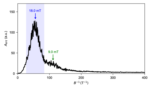
Supplementary Note 4. Additional data in the multi-path Aharonov-Bohm regime
Two methods were used to study the phase evolution of the magneto-conductance oscillations for the device discussed in the main text. The data shown in Figs. 4 and 5 are taken by sweeping as the fast axis and as the slow axis. Oppositely, in Supplementary Figure 4 we present data taken with and being the fast and slow axis, respectively. The data presented here are taken at V as in Fig. 4 of the main text. For each value of (proportional to ) the maxima of the AB oscillations are tracked, and their positions in are converted into the transmission phase via the AB periodicity and plotted in Supplementary Figure 4a. In Supplementary Figure 4b, we show the corresponding conductance trace (blue data points) exhibiting CPs. The phase displays a rapid evolution close to the charge degeneracy points. At the two inner CPs, the phase evolves by , and gradually shifts back to the original value. For the first and fourth CPs, the variation is much smaller than . For all displayed Coulomb valleys, the phase is neither constant, nor does it exhibit a rapid phase lapse. Instead, gradual variations are observed, compatible with the picture discussed in the main text in which multiple trajectories with different enclosed areas in the nanowire interferometer couple to different QD orbitals.
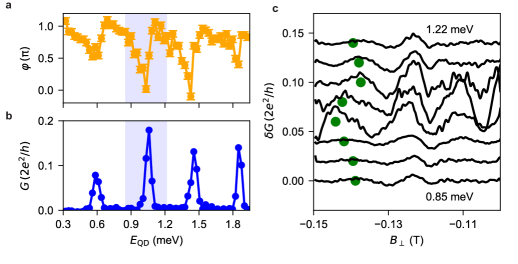
Supplementary Note 5. Phase variations and fundamental symmetries
The top panel of Fig. 4d in the main text shows that the transmission phase swings from to at resonance over an energy range of . This continuous variation differs significantly from what has been reported in the pioneering experiment of ref. YAC1995 where the phase was mysteriously locked to and with abrupt switches in between. Later on, their finding was understood in term of fundamental symmetries.
Time-reversal symmetry imposes, in fact, the two-terminal conductance to be an even function of the magnetic field (the Casimir-Onsager relation: ). In an Aharonov-Bohm interferometer, the conductance displays sinusoidal oscillations on top of a background, and the symmetry around zero field imposes on their phase to assume only two values: or . However, in our experiment we find the opposite: the phase variation at resonance is smooth and not abrupt. We associate this behaviour with the fact that time-reversal symmetry does not hold in our context due to the large magnetic fields applied.
Supplementary Note 6. Fitting results
VI.1 Main text Fig. 3
We obtain the dashed lines in Fig. 3a by fitting each peak independently with the single-trajectory model Aharonov-Bohm interferometer. For this and other fits, we use and similarly to ref. AHA2005. The phase of is a fitting parameter that is not relevant and therefore not displayed. We report the other values in Supplementary Table 1 subdivided into the three characteristic regimes in Fig. 3a.
| Regime | |||
|---|---|---|---|
| Average parameter | low (green trace) | medium (blue trace) | high (orange trace) |
VI.2 Main text Fig. 4
We obtain Fig. 4b by fitting the data of Fig. 4a with the single-trajectory model Aharonov-Bohm interferometer with . The fitting procedure is facilitated by fixing two parameters globally (i.e., for the entire measurement): a constant offset to the traces of and . The phase of is an independent parameter that increases with the magnetic field along the y-axis. We display in Supplementary Table 2 the best-fit parameters averaged along the magnetic field axis. Peak numbers are ordered from left to right.
| Peak number | ||
|---|---|---|
| Average parameter | ||
VI.3 Main text Fig. 5
In order to obtain Fig. 5b of the main text, we first consider the line-cut of the data at T and fit the peaks independently with the single-path interferometer model. We fix some of the parameters to simplify the procedure as and the added offset to the trace at . In this procedure, the phase of is used as a free parameter and not relevant here. The other values are shown in Supplementary Table 3, where the peak names in Fig. 5a are ordered numerically from left to right.
We then extrapolate the trace with the best-fit parameters by varying the phase of and adjusting the values of to qualitatively reproduce the experimental data.
| Peak number | ||||
|---|---|---|---|---|
| Parameter | 1 | 2 | 3 | 4 |
Supplementary Note 7. Cotunnelling Aharonov-Bohm effect in a second device
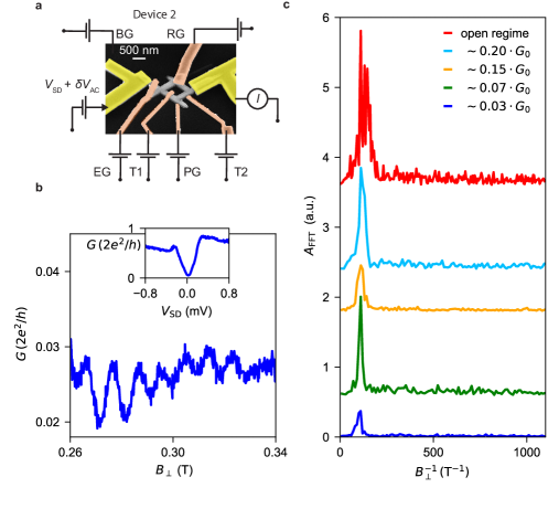
Here, we report additional measurements of Aharonov-Bohm interference in the cotunnelling regime for a second device. The electron density in this device (Supplementary Figure 5a) is tunable by voltages on a global back gate and several top gates. The top dielectric used here is grown via atomic layer deposition. A T-shaped quantum dot is formed in the bottom branch of the interferometer and has a charging energy of meV, with the tunnel coupling to the leads adjustable using the tunnel gates T1 and T2. Although the conductance around is strongly suppressed owing to the Coulomb blockade (inset of Supplementary Figure 5b), the magneto-conductance exhibits clear Aharonov-Bohm oscillations with a periodicity of mT (Supplementary Figure 5b, main panel). The oscillation amplitude is sizable despite the cotunnelling conductance being as low as . This value corresponds to a typical dwell time in the QD in the order of ps. The magnitude of the Fast Fourier Transform (FFT) of these oscillations is displayed in Supplementary Figure 5c, together with the FFTs of the AB oscillations at gradually stronger cotunnelling conductance, until the Coulomb blockade is fully quenched (red trace corresponding to the ’open regime’ with ). We observe here that the width of the FFT peak of the AB signal increases when quenching the Coulomb blockade by making the barriers more transparent (in particular, see the difference between the red and the other traces). This fact might suggest that, when the quantum dot is defined, fewer trajectories play a role in the transport through the interferometer, reducing the spread of the enclosed area.
Supplementary Note 8. Temperature dependence of the Aharonov-Bohm effect
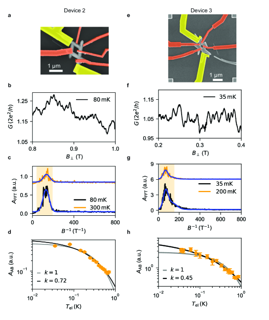
In Supplementary Figures 6a and 6e, we show the scanning electron micrographs of two nanowire loops (second and third devices) used to study the temperature dependence of the Aharonov-Bohm oscillations. In Supplementary Figures 6b and 6f, we plot two typical magneto-conductance traces of each device. They both exhibit AB oscillations superimposed on a slowly varying background. In the data analysis, we subtract this background and calculate the Fast Fourier Transform. The amplitudes shown in Figs. 6c and 6g are the averaged Fast Fourier Transforms of several scans taken in the same magnetic field window. The peaks in the spectra are fitted with a Gaussian obtaining the power spectrum of the AB oscillations . For the third device, we find that the sum of two Gaussian curves better describes the broad FFT peak due to the presence of the second harmonic. In panels d and h, we demonstrate the decrease of as a function of temperature. The amplitudes of each harmonic (with index ) are expected to decrease as , with being the phase coherence length and being the effectively travelled path length IHN2010. In ballistic systems, we have , while in the diffusive regime LUD2004.
We fitted the experimental decay of the Aharonov-Bohm amplitude with the function , with free parameters , , , and the Aharonov-Bohm phase coherence length defined as . The best-fit curves are shown in black, and correspond to and for the second and third devices, respectively. For comparison, we also show the best-fit curves obtained for . The values of the fitted exponents reflect the nature of the transport in the semiconducting loops, which is in the crossover between completely ballistic and diffusive. In fact, the typically travelled length is m, which is only a few times larger than the estimated mean free path of m VAN2015; GUL2015. We expect that at higher temperatures and for the longer loops (cf. device 2) the diffusive model with captures the experimental trend better than the ballistic one, but the experimental data do not provide conclusive evidence.
From our analysis, we derive m for the second device, and m for the third loop. It can be argued that these values are probably underestimating the actual coherence length since the amplitude of the AB oscillations (more generally all odd harmonics) are additionally suppressed by the energy averaging effect.
Supplementary References
- (1) Yacoby, A., Heiblum, M., Mahalu, D. & Shtrikman, H. Coherence and phase sensitive measurements in a quantum dot. Phys. Rev. Lett. 74, 4047–4050 (1995).
- (2) Aharony, A., Entin-Wohlman, O. & Imry, Y. Phase measurements in open and closed Aharonov-Bohm interferometers. Phys. E 29, 283 – 288 (2005).
- (3) Ihn, T. Semiconductor Nanostructures (Oxford University Press, 2010).
- (4) Ludwig, T. & Mirlin, A. D. Interaction-induced dephasing of Aharonov-Bohm oscillations. Phys. Rev. B 69, 193306 (2004).
- (5) van Weperen, I. et al. Spin-orbit interaction in InSb nanowires. Phys. Rev. B 91, 201413 (2015).
- (6) Ö. Gül et al. Towards high mobility InSb nanowire devices. Nanotechnology 26, 215202 (2015).