Using nonlocal surface transport to identify the axion insulator
Abstract
The axion is a hypothetical but experimentally undetected particle. Recently, the antiferromagnetic topological insulator MnBi2Te4 has been predicted to host the axion insulator, but the experimental evidence remains elusive. Specifically, the axion insulator is believed to carry “half-quantized” chiral currents running antiparallel on its top and bottom surfaces. However, it is challenging to measure precisely the half-quantization. Here, we propose a nonlocal surface transport device, in which the axion insulator can be distinguished from normal insulators without a precise measurement of the half-quantization. More importantly, we show that the nonlocal surface transport, as a qualitative measurement, is robust in realistic situations when the gapless side surfaces and disorder come to play. Moreover, thick electrodes can be used in the device of MnBi2Te4 thick films, enhancing the feasibility of the surface measurements. This proposal will be insightful for the search of the axion insulator and axion in topological matter.
blueIntroduction.– The axion is an elementary particle postulated to resolve the strong CP problem in quantum chromodynamics, but remains invisible in experiments Peccei and Quinn (1977). In recent years, the axion insulator in condensed matter physics has attracted great attention because it shares the axionic electromagnetic response Mogi et al. (2017a, b); Xiao et al. (2018); Varnava and Vanderbilt (2018); Liu and Wang (2020); Xu et al. (2019), which modifies Maxwell’s equations and may lead to a “half-quantized” surface Hall conductance Essin et al. (2009); Mong et al. (2010); Niu et al. (2020); Xu et al. (2014) or the topological magnetoelectric effect Wang et al. (2015a); Morimoto et al. (2015); Qi et al. (2009); Maciejko et al. (2010); Tse and MacDonald (2010); Yu et al. (2019). Unfortunately, these signatures require highly demanding precisions of measurement and device fabrication, so the experimental attempts to identify the axion insulator have yet to be successful Liu and Wang (2020); Varnava and Vanderbilt (2018) (see also Sec. IX of Sup ). Recently, in the experiments of the first antiferromagnetic topological insulator MnBi2Te4 Chang et al. (2013); Yu et al. (2010); Zhang et al. (2019a); Wang et al. (2015b); Ding et al. (2020); Zhang et al. (2019b); Li et al. (2019a); Otrokov et al. (2019a, b); Deng et al. (2020a); Liu et al. (2020); Gong et al. (2019); Zhang et al. (2020); Li et al. (2019b); Shi et al. (2019); Chen et al. (2019); Hao et al. (2019); Sun et al. (2019); Jo et al. (2019), the signatures for the quantized anomalous Hall effect and axion insulator have been reported Deng et al. (2020a); Liu et al. (2020). Specifically, the axion (Chern) insulator has antiparallel (parallel) chiral currents on the top and bottom surfaces. Each current is responsible for the Hall conductance. The top and bottom chiral currents combine to yield a zero () Hall conductance as a signature for the axion (Chern) insulator [Figs. 1(a)-(b)]. The Chern and axion insulators may be distinguished by optical measurements Pozo et al. (2019). However, normal insulators also have a zero Hall conductance [Fig. 1(c)]. Therefore, seeking signatures for the axion insulator is still an open problem.
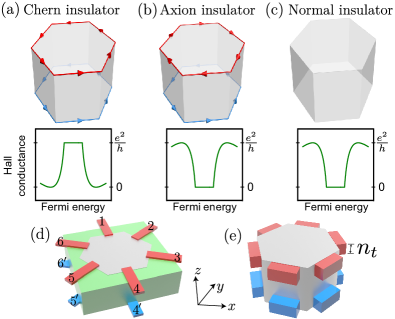
In this Letter, we propose that the axion insulator can be distinguished from normal insulators by measuring nonlocal surface resistances in a device of the antiferromagnetic topological insulator MnBi2Te4 [Fig. 1(d)]. MnBi2Te4 is formed by stacked septuple layers with out-of-plane magnetization. The neighbouring septuple layers have opposite magnetizations. For even (odd) layers, the chiral currents on the top and bottom surfaces propagate along the opposite (same) directions [Figs. 1(a)-(b)], forming an axion insulator (a thick Chern insulator). Because of the chiral currents, the axion insulator shows distinct nonlocal surface transport, compared to those in the Chern insulator and normal insulator. We numerically calculate the nonlocal surface transport of MnBi2Te4 with different septuple layers by using a lattice model and realistic parameters. More importantly, we show that the nonlocal surface transport, as a qualitative measurement, is robust against disorder andside-surface transport. Moreover, we show that thick films of MnBi2Te4 allow thick electrodes to measure the surface transport [Fig. 1(e)]. Therefore, the nonlocal surface transport provides a feasible approach to identify the axion insulator. Our results will be helpful for the ongoing and future search for the axion insulator.
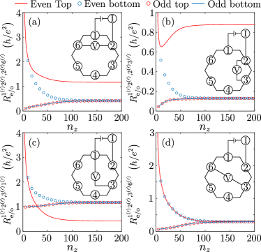
blueNonlocal surface transport.– The axion insulator is characterized by the opposite “half-quantized” chiral currents [Fig. 1(b)] due to its axion electromagnetic response. Detecting the chiral current can help to identify the axion insulator. Compared to the ultrathin films of magnetically-doped Bi2Se3-like materials, bulk crystals of intrinsic antiferromagnetic insulator MnBi2Te4 can be used directly for measurements, and allow electrodes to probe mostly the top or bottom surface, respectively, as shown in Fig. 1(d). Usually, a direct probe of the chiral currents is prohibited by the side surfaces, which have metallic surface states that bury the signals of the chiral currents. To solve this problem, we introduce the nonlocal surface measurements. The metallic states on the side surfaces are not chiral, that is, they go opposite directions with the same weight, thus do not play a significant role in the nonlocal transport compared to the chiral currents. Specifically, the top (bottom) surface of the device has six electrodes, - (-) [Fig. 1(d)]. As shown in Fig. 2, a current is applied between electrodes 1 and 2 ( and ) on the top (bottom) surface, and a nonlocal voltage is measured between other two electrodes on the same surface, to define a nonlocal resistance Roth et al. (2009).
For a given surface, the nonlocal resistances can be analytically Datta (1997) found for the 4 configurations in Fig. 2 as
| (1) |
with and . Here, and determine the matrix elements the transmission probability matrices (details and more configurations can be found in Sec. SII of Sup ).
Before considering realistic situations with side surfaces, disorder, and thick electrodes, we first use ideal cases for illustration. For odd layers, the half-quantized chiral currents on the top and bottom surfaces are parallel, i.e., and for both top and bottom surfaces. For even layers, the half-quantized chiral currents are opposite, i.e., and on the top and and on the bottom surface. Table 1 shows the the ideal nonlocal resistances for the configurations in Fig. 2. For odd layers, the two surfaces always have the same nonlocal resistance. For even layers, the nonlocal resistances on the two surfaces have different values for most of the cases, except for the case with . Therefore, the axion insulator in even layers and Chern insulator in odd layers would show distinct nonlocal surface transport properties. More importantly, the normal insulator has no such nonlocal resistance because it has no chiral current (see Fig. 1(c) and Sec. SVI of Sup ). Therefore, the unique nonlocal resistance can be used to distinguish the axion insulator from normal insulators. Above are the ideal cases. In real materials with side surfaces, disorder, and thick electrodes, the chiral currents and are not perfectly half-quantized. Below we will verify the above proposal by using a realistic model and simulations.
| 2 | 0 | 2 | 0 | |
| 0 | 2 | 0 | 0 | |
| 0 | 2 | 0 | 0 | |
| 0 | 2 | 0 | 0 |
blueModel.– For numerical calculations, we use an effective model for MnBi2Te4 regularized on a stacked hexagonal lattice Zhang et al. (2020)
| (2) |
with the intra-layer part = - + + + + + + - , the inter-layer part + . The lattice constants . The wave vectors , , . is the identity matrix, for , , , and . and are the Pauli matrices. with angles and for . The antiferromagnetic order is described by and . For a realistic simulation, we use the parameters transformed from those in the model Zhang et al. (2019b); Sup , , eV, eVÅ2, eVÅ2, eVÅ, eVÅ, and eV, which describes the A-type antiferromagnetic topological insulator in MnBi2Te4.
The model describes a topological insulator with two gapped surface states on the top and bottom surfaces (Fig. S1(b) of Sup ), due to breaking of the combined antiferromagnetic time-reversal symmetry . The gapped surfaces behave like “marginal” 2D Chern insulators, characterized by “half-quantized” chiral currents (Fig. 1), in a sense that their Chern numbers are half-quantized as , or in other words the Hall conductance [see, e.g., Fig. 3 (a) as ]. The sign depends on the magnetization, which reverses from one septuple layer to another in MnBi2Te4 Mong et al. (2010); Li et al. (2019a). For odd (even) layers, the top and bottom surfaces have the same (opposite) magnetization, so the half-quantized surface Hall conductances of the top and bottom surfaces add up (cancel) to give a Chern insulator characterized by (axion insulator with ) Zhang et al. (2019b); Li et al. (2019a); Otrokov et al. (2019a, b); Deng et al. (2020a); Liu et al. (2020); Gong et al. (2019); Zhang et al. (2020); Li et al. (2019b); Shi et al. (2019); Chen et al. (2019); Hao et al. (2019) (see also Fig. S1(c) of Sup ). The chiral currents, which are responsible for the half-quantized surface Hall conductance, can be numerically verified using first-principles calculations for MnBi2Te4 Gu et al. (2020).
blueCalculation of the nonlocal surface transport.–We calculate the nonlocal surface transport Chu et al. (2011) by using the Landauer-Büttiker-Fisher-Lee formula Landauer (1970); Büttiker (1988); Fisher and Lee (1981) and the recursive Green’s function method MacKinnon (1985); Metalidis and Bruno (2005). At zero temperature, the current flowing into electrode is given by
| (3) |
where is the voltage at electrode , is the transmission coefficient from electrode to . For the present case, there are 6 electrodes for each of top and bottom surfaces, so is a 66 matrix (more details can be found in Sec. SII and Sec. SVI of Sup ).
Figure 2 shows the numerically calculated nonlocal resistances for 4 configurations as functions of film thickness (number of septuple layers ). In odd layers, the resistances have the same values for the top and bottom surfaces. In even layers, the resistances have distinct values for the two surfaces, except for those in Fig. 2(d). For thick films in Fig. 2, there are deviations from the analytic values in Tab. 1. This is due to the gapless side surface states Chu et al. (2011), and is one of the reasons why it is hard to measure the half-quantized Hall effect as the signature for the axion insulator. Later, we will show the nonlocal surface transport, as a qualitative measurement, is robust against not only the side-surface transport but also disorder and thick electrodes.
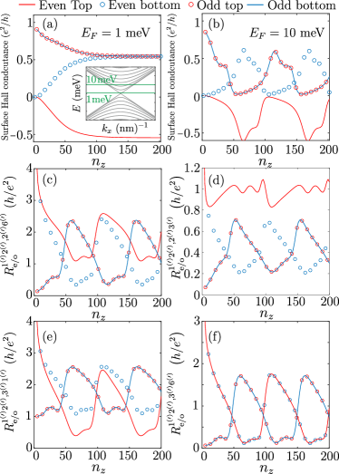
blueSide-surface effects.– Figures 3(a-b) show the numerical results of the surface Hall conductance for different , which can be found from the left-chiral and right-chiral currents, e.g., for the top surface in even layers. For the ideal case, the top and bottom surface Hall conductances are half-quantized (), and reduce to 0 and as for even and odd layers, respectively, as a result of the top-bottom hybridization Zhou et al. (2008); Lu et al. (2010); Linder et al. (2009); Zhang et al. (2010); Chen and Zhou (2016); Liu et al. (2010); Imura et al. (2012); Takane (2016); Chen et al. (2017). A zoom-in of Figure 3(a) shows that the surface Hall conductances are not precisely half-quantized due to the coupling of the side surface states when the Fermi energy is away from the Dirac point. This shows that a direct measurement of the half-quantized Hall effect is challenging, in accordance with the previous studies König et al. (2014). Figure 3(b) shows that the side surface states turn the surface Hall conductance into an oscillation with at higher Fermi energies ( meV), as a result of the confinement-induced subbands of the side surface states [inset of Fig. 3(a)]. Similar oscillations also present in the nonlocal surface transport in Figs. 3(c-f).
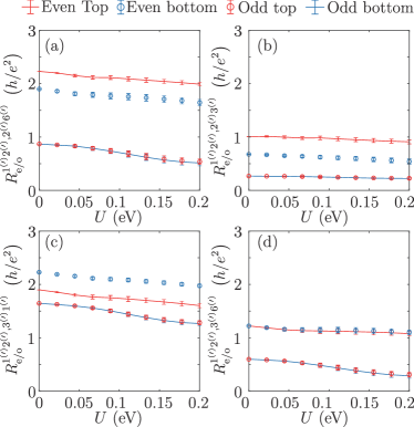
blueDisorder effects. – Now, we show that the nonlocal surface transport is robust against disorder. We introduce the Anderson-type disorder to the central scattering region with , where is uniformly distributed within , with being the disorder strength. In Fig. 4, we show the nonlocal surface resistance as functions of the disorder strength for and with the side surfaces ( meV). Even for strong disorder ( eV, about the size of the bulk band gap), the nonlocal resistances remain at the same order of magnitude.
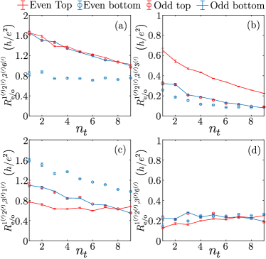
blueThick electrodes. – Above, we assume that the electrodes are only attached to the topmost and bottommost septuple layers of the device. Figure 5 shows the numerical results for thick electrodes [Fig. 1(e)]. We consider a realistic situation in which the side surface states ( meV) and disorder ( meV) are also taken into account. The nonlocal resistances drop with increasing electrode thickness (), but stay at the same order of magnitude up to 10 septuples (about 14 nm, thicker than the thinnest metal electrode that can be fabricated). The chiral nature of the surface transport for even and odd layers are still stable with increasing the electrode thickness, showing the topological nature of the chiral currents.
blueDiscussion and experimental realization.– In this work, we focus on distinguishing the axion insulator and normal insulator, by using the nonlocal signal. If and only if the system is an axion insulator, the nonlocal resistances are significantly different on the top and bottom surfaces. Furthermore, we also calculated the surface transport coefficients for those systems without the chiral hinge currents, including the topological insulator, Weyl semimetal, and Dirac semimetal (see Sec. SVI of Sup ). Our calculations show that, the nonlocal signals in the axion insulator are absent in other systems without the chiral hinge currents. Moreover, the propagation directions of surface chiral states can be identified if the nonlocal resistances can be measured by using properly chosen combinations of the measurement electrodes, e.g., those in Figs. 2 (a-c) (more details can be found in Sec. SII of Sup ).
Finally, we discuss how to realize the nonlocal surface measurement in Fig. 1(d) with the help of the existing nanotechnologies. We propose the following fabrication process flow. The bottom graphite electrodes can be prepatterned by electron beam lithography and plasma etching on Si/SiO2 wafers. To ensure the contact, the polymer residues on the graphite electrodes need to be removed by forming gas annealing in Ar/H2 environment. Thin flakes of MnBi2Te4 are mechanically exfoliated. Flakes with preferred thickness (e.g., 200 nm) and flatness can be selected by atomic force microscopy, then laminated to the prepatterned bottom electrodes via polymer-assisted dry transfer technique. Moreover, the quantum anomalous Hall effect has been reported in a MnBi2Te4/Bi2Te3 superlattice of a thickness up to 300 nm, in which the Fermi level is efficiently tuned in the surface gap Deng et al. (2020b). To electrically separate the bottom electrodes and avoid contact on the side edges of MnBi2Te4, lithography free contact in Ref. Telford et al. (2018) can be used. Such electrodes can be thin and flat so that it is non-invasive for probing just the surface septuple layer. The process involving MnBi2Te4 thin flakes has to be protected by an inert gas environment such as a glove-box, as surface reconstructions may occur Hou et al. (2020). Therefore, all of these nanotechnologies have been there, offering the possibility of detecting the axion insulator.
Acknowledgements.
We thank helpful discussions with Jianpeng Liu, Chuizhen Chen, Hua Jiang, Donghui Xu and Bin Zhou. This work was supported by the National Natural Science Foundation of China (11534001, 11974249, 11925402), the Strategic Priority Research Program of Chinese Academy of Sciences (Grant No. XDB28000000), Guangdong province (2016ZT06D348), the National Key R & D Program (2016YFA0301700), the Natural Science Foundation of Shanghai (Grant No. 19ZR1437300), Shenzhen High-level Special Fund (No. G02206304, G02206404), and the Science, Technology and Innovation Commission of Shenzhen Municipality (ZDSYS20190902092905285, ZDSYS20170303165926217, JCYJ20170412152620376, KYTDPT20181011104202253). R.C. acknowledges support from the project funded by the China Postdoctoral Science Foundation (Grant No. 2019M661678) and the SUSTech Presidential Postdoctoral Fellowship. The numerical calculations were supported by Center for Computational Science and Engineering of Southern University of Science and Technology.References
- Peccei and Quinn (1977) R. D. Peccei and H. R. Quinn, “CP conservation in the presence of pseudoparticles”, Phys. Rev. Lett. 38, 1440 (1977).
- Mogi et al. (2017a) M. Mogi, M. Kawamura, R. Yoshimi, A. Tsukazaki, Y. Kozuka, N. Shirakawa, K. S. Takahashi, M. Kawasaki, and Y. Tokura, “A magnetic heterostructure of topological insulators as a candidate for an axion insulator”, Nat. Mater. 16, 516 (2017a).
- Mogi et al. (2017b) M. Mogi, M. Kawamura, A. Tsukazaki, R. Yoshimi, K. S. Takahashi, M. Kawasaki, and Y. Tokura, “Tailoring tricolor structure of magnetic topological insulator for robust axion insulator”, Sci. Adv. 3, eaao1669 (2017b).
- Xiao et al. (2018) D. Xiao, J. Jiang, J.-H. Shin, W. Wang, F. Wang, Y.-F. Zhao, et al., “Realization of the axion insulator state in quantum anomalous Hall sandwich heterostructures”, Phys. Rev. Lett. 120, 056801 (2018).
- Varnava and Vanderbilt (2018) N. Varnava and D. Vanderbilt, “Surfaces of axion insulators”, Phys. Rev. B 98, 245117 (2018).
- Liu and Wang (2020) Z. Liu and J. Wang, “Anisotropic topological magnetoelectric effect in axion insulators”, Phys. Rev. B 101, 205130 (2020).
- Xu et al. (2019) Y. Xu, Z. Song, Z. Wang, H. Weng, and X. Dai, “Higher-order topology of the axion insulator EuIn2As2”, Phys. Rev. Lett. 122, 256402 (2019).
- Essin et al. (2009) A. M. Essin, J. E. Moore, and D. Vanderbilt, “Magnetoelectric polarizability and axion electrodynamics in crystalline insulators”, Phys. Rev. Lett. 102, 146805 (2009).
- Mong et al. (2010) R. S. K. Mong, A. M. Essin, and J. E. Moore, “Antiferromagnetic topological insulators”, Phys. Rev. B 81, 245209 (2010).
- Niu et al. (2020) C. Niu, H. Wang, N. Mao, B. Huang, Y. Mokrousov, and Y. Dai, “Antiferromagnetic topological insulator with nonsymmorphic protection in two dimensions”, Phys. Rev. Lett. 124, 066401 (2020).
- Xu et al. (2014) Y. Xu, I. Miotkowski, C. Liu, J. Tian, H. Nam, N. Alidoust, J. Hu, C.-K. Shih, M. Z. Hasan, and Y. P. Chen, “Observation of topological surface state quantum Hall effect in an intrinsic three-dimensional topological insulator”, Nature Phys. 10, 956 (2014).
- Wang et al. (2015a) J. Wang, B. Lian, X.-L. Qi, and S.-C. Zhang, “Quantized topological magnetoelectric effect of the zero-plateau quantum anomalous Hall state”, Phys. Rev. B 92, 081107(R) (2015a).
- Morimoto et al. (2015) T. Morimoto, A. Furusaki, and N. Nagaosa, “Topological magnetoelectric effects in thin films of topological insulators”, Phys. Rev. B 92, 085113 (2015).
- Qi et al. (2009) X.-L. Qi, R. Li, J. Zang, and S.-C. Zhang, “Inducing a magnetic monopole with topological surface states”, Science 323, 1184 (2009).
- Maciejko et al. (2010) J. Maciejko, X.-L. Qi, H. D. Drew, and S.-C. Zhang, “Topological quantization in units of the fine structure constant”, Phys. Rev. Lett. 105, 166803 (2010).
- Tse and MacDonald (2010) W.-K. Tse and A. H. MacDonald, “Giant magneto-optical Kerr effect and universal Faraday effect in thin-film topological insulators”, Phys. Rev. Lett. 105, 057401 (2010).
- Yu et al. (2019) J. Yu, J. Zang, and C.-X. Liu, “Magnetic resonance induced pseudoelectric field and giant current response in axion insulators”, Phys. Rev. B 100, 075303 (2019).
- (18) See Supplemental Material for more details of the effective model, nonlocal transport, finite size effect on the - plane, disorder effects for other configurations, current distribution, and surface transport for topological and normal insulators, which includes Refs. Zhang et al. (2020, 2019b); Bernevig and Hughes (2013); Chiu et al. (2016); Shen (2017); Li et al. (2019a); Otrokov et al. (2019a); Chu et al. (2011); Landauer (1970); Büttiker (1988); Fisher and Lee (1981); MacKinnon (1985); Metalidis and Bruno (2005); Roth et al. (2009); Zhou et al. (2008); Kobayashi et al. (2013); Hattori and Okamoto (2016); Yang et al. (2011); Chen et al. (2015, 2018); Varnava and Vanderbilt (2018); Mong et al. (2010); Xiao et al. (2018); Mogi et al. (2017b, a); Wang et al. (2015a); Morimoto et al. (2015); Qi et al. (2009); Maciejko et al. (2010); Tse and MacDonald (2010); Yu et al. (2019); Qi et al. (2008); Pan et al. (2020) .
- Chang et al. (2013) C.-Z. Chang, J. Zhang, X. Feng, J. Shen, Z. Zhang, M. Guo, et al., “Experimental observation of the quantum anomalous Hall effect in a magnetic topological insulator”, Science 340, 167 (2013).
- Yu et al. (2010) R. Yu, W. Zhang, H.-J. Zhang, S.-C. Zhang, X. Dai, and Z. Fang, “Quantized anomalous Hall effect in magnetic topological insulators”, Science 329, 61 (2010).
- Zhang et al. (2019a) J. Zhang, Z. Liu, and J. Wang, “In-plane magnetic-field-induced quantum anomalous Hall plateau transition”, Phys. Rev. B 100, 165117 (2019a).
- Wang et al. (2015b) J. Wang, B. Lian, and S.-C. Zhang, “Quantum anomalous Hall effect in magnetic topological insulators”, Phys. Scr. T164, 014003 (2015b).
- Ding et al. (2020) Y.-R. Ding, D.-H. Xu, C.-Z. Chen, and X. C. Xie, “Hinged quantum spin Hall effect in antiferromagnetic topological insulators”, Phys. Rev. B 101, 041404(R) (2020).
- Zhang et al. (2019b) D. Zhang, M. Shi, T. Zhu, D. Xing, H. Zhang, and J. Wang, “Topological axion states in the magnetic insulator MnBi2Te4 with the quantized magnetoelectric effect”, Phys. Rev. Lett. 122, 206401 (2019b).
- Li et al. (2019a) J. Li, Y. Li, S. Du, Z. Wang, B.-L. Gu, S.-C. Zhang, K. He, W. Duan, and Y. Xu, “Intrinsic magnetic topological insulators in van der Waals layered MnBi2Te4-family materials”, Sci. Adv. 5, eaaw5685 (2019a).
- Otrokov et al. (2019a) M. M. Otrokov, I. P. Rusinov, M. Blanco-Rey, M. Hoffmann, A. Y. Vyazovskaya, S. V. Eremeev, A. Ernst, P. M. Echenique, A. Arnau, and E. V. Chulkov, “Unique thickness-dependent properties of the van der Waals interlayer antiferromagnet MnBi2Te4 films”, Phys. Rev. Lett. 122, 107202 (2019a).
- Otrokov et al. (2019b) M. M. Otrokov, I. I. Klimovskikh, H. Bentmann, D. Estyunin, A. Zeugner, Z. S. Aliev, et al., “Prediction and observation of an antiferromagnetic topological insulator”, Nature 576, 416 (2019b).
- Deng et al. (2020a) Y. Deng, Y. Yu, M. Z. Shi, Z. Guo, Z. Xu, J. Wang, X. H. Chen, and Y. Zhang, “Quantum anomalous Hall effect in intrinsic magnetic topological insulator MnBi2Te4”, Science 367, 895 (2020a).
- Liu et al. (2020) C. Liu, Y. Wang, H. Li, Y. Wu, Y. Li, J. Li, K. He, Y. Xu, J. Zhang, and Y. Wang, “Robust axion insulator and Chern insulator phases in a two-dimensional antiferromagnetic topological insulator”, Nature Mater. 19, 522 (2020).
- Gong et al. (2019) Y. Gong, J. Guo, J. Li, K. Zhu, M. Liao, X. Liu, et al., “Experimental realization of an intrinsic magnetic topological insulator”, Chin. Phys. Lett. 36, 076801 (2019).
- Zhang et al. (2020) R.-X. Zhang, F. Wu, and S. Das Sarma, “Möbius Insulator and Higher-Order Topology in ”, Phys. Rev. Lett. 124, 136407 (2020).
- Li et al. (2019b) Y. Li, Z. Jiang, J. Li, S. Xu, and W. Duan, “Magnetic anisotropy of the two-dimensional ferromagnetic insulator MnBi2Te4”, Phys. Rev. B 100, 134438 (2019b).
- Shi et al. (2019) M. Z. Shi, B. Lei, C. S. Zhu, D. H. Ma, J. H. Cui, Z. L. Sun, J. J. Ying, and X. H. Chen, “Magnetic and transport properties in the magnetic topological insulators MnBi2Te4(Bi2Te3)n”, Phys. Rev. B 100, 155144 (2019).
- Chen et al. (2019) Y. J. Chen, L. X. Xu, J. H. Li, Y. W. Li, H. Y. Wang, C. F. Zhang, et al., “Topological electronic structure and its temperature evolution in antiferromagnetic topological insulator MnBi2Te4”, Phys. Rev. X 9, 041040 (2019).
- Hao et al. (2019) Y.-J. Hao, P. Liu, Y. Feng, X.-M. Ma, E. F. Schwier, M. Arita, et al., “Gapless surface Dirac cone in antiferromagnetic topological insulator MnBi2Te4”, Phys. Rev. X 9, 041038 (2019).
- Sun et al. (2019) H. Sun, B. Xia, Z. Chen, Y. Zhang, P. Liu, Q. Yao, H. Tang, Y. Zhao, H. Xu, and Q. Liu, “Rational design principles of the quantum anomalous Hall effect in superlatticelike magnetic topological insulators”, Phys. Rev. Lett. 123, 096401 (2019).
- Jo et al. (2019) N. H. Jo, L.-L. Wang, R.-J. Slager, J. Yan, Y. Wu, K. Lee, B. Schrunk, A. Vishwanath, and A. Kaminski, “Intrinsic axion insulating behavior in antiferromagnetic MnBi6Te10”, arXiv:1910.14626 (2019).
- Pozo et al. (2019) O. Pozo, C. Repellin, and A. G. Grushin, “Quantization in chiral higher order topological insulators: Circular dichroism and local chern marker”, Phys. Rev. Lett. 123, 247401 (2019).
- Roth et al. (2009) A. Roth, C. Brune, H. Buhmann, L. W. Molenkamp, J. Maciejko, X.-L. Qi, and S.-C. Zhang, “Nonlocal transport in the quantum spin Hall state”, Science 325, 294 (2009).
- Datta (1997) S. Datta, Electronic Transport in Mesoscopic Systems (Cambridge University Press, 1997).
- Gu et al. (2020) M. Gu, J. Li, H. Sun, Y. Zhao, C. Liu, J. Liu, and Q. Liu, “Half-quantized anomalous Hall effect in magnetic axion insulator MnBi2Te4/(Bi2Te3)n”, arXiv:2005.13943 (2020).
- Chu et al. (2011) R.-L. Chu, J. Shi, and S.-Q. Shen, “Surface edge state and half-quantized Hall conductance in topological insulators”, Phys. Rev. B 84, 085312 (2011).
- Landauer (1970) R. Landauer, “Electrical resistance of disordered one-dimensional lattices”, Philos. Mag. 21, 863 (1970).
- Büttiker (1988) M. Büttiker, “Absence of backscattering in the quantum Hall effect in multiprobe conductors”, Phys. Rev. B 38, 9375 (1988).
- Fisher and Lee (1981) D. S. Fisher and P. A. Lee, “Relation between conductivity and transmission matrix”, Phys. Rev. B 23, 6851 (1981).
- MacKinnon (1985) A. MacKinnon, “The calculation of transport properties and density of states of disordered solids”, Z. Phys. B 59, 385 (1985).
- Metalidis and Bruno (2005) G. Metalidis and P. Bruno, “Green’s function technique for studying electron flow in two-dimensional mesoscopic samples”, Phys. Rev. B 72, 235304 (2005).
- Zhou et al. (2008) B. Zhou, H.-Z. Lu, R.-L. Chu, S.-Q. Shen, and Q. Niu, “Finite size effects on helical edge states in a quantum spin-Hall system”, Phys. Rev. Lett. 101, 246807 (2008).
- Lu et al. (2010) H. Z. Lu, W. Y. Shan, W. Yao, Q. Niu, and S. Q. Shen, “Massive Dirac fermions and spin physics in an ultrathin film of topological insulator”, Phys. Rev. B 81, 115407 (2010).
- Linder et al. (2009) J. Linder, T. Yokoyama, and A. Sudbø, “Anomalous finite size effects on surface states in the topological insulator Bi2Se3”, Phys. Rev. B 80, 205401 (2009).
- Zhang et al. (2010) Y. Zhang, K. He, C.-Z. Chang, C.-L. Song, L.-L. Wang, X. Chen, et al., “Crossover of the three-dimensional topological insulator Bi2Se3 to the two-dimensional limit”, Nature Phys. 6, 584 (2010).
- Chen and Zhou (2016) R. Chen and B. Zhou, “Finite size effects on the helical edge states on the Lieb lattice”, Chin. Phys. B 25, 067204 (2016).
- Liu et al. (2010) C.-X. Liu, X.-L. Qi, H. J. Zhang, X. Dai, Z. Fang, and S.-C. Zhang, “Model Hamiltonian for topological insulators”, Phys. Rev. B 82, 045122 (2010).
- Imura et al. (2012) K.-I. Imura, M. Okamoto, Y. Yoshimura, Y. Takane, and T. Ohtsuki, “Finite-size energy gap in weak and strong topological insulators”, Phys. Rev. B 86, 245436 (2012).
- Takane (2016) Y. Takane, “Disorder effect on chiral edge modes and anomalous Hall conductance in Weyl semimetals”, J. Phys. Soc. Jpn. 85, 124711 (2016).
- Chen et al. (2017) R. Chen, D.-H. Xu, and B. Zhou, “Topological Anderson insulator phase in a Dirac-semimetal thin film”, Phys. Rev. B 95, 245305 (2017).
- König et al. (2014) E. J. König, P. M. Ostrovsky, I. V. Protopopov, I. V. Gornyi, I. S. Burmistrov, and A. D. Mirlin, “Half-integer quantum Hall effect of disordered Dirac fermions at a topological insulator surface”, Phys. Rev. B 90, 165435 (2014).
- Deng et al. (2020b) H. Deng, Z. Chen, A. Wołoś, M. Konczykowski, K. Sobczak, J. Sitnicka, et al., “High-temperature quantum anomalous Hall regime in a MnBi2Te4/Bi2Te3 superlattice”, Nat. Phys. 17, 36 (2020b).
- Telford et al. (2018) E. J. Telford, A. Benyamini, D. Rhodes, D. Wang, Y. Jung, A. Zangiabadi, et al., “Via method for lithography free contact and preservation of 2D materials”, Nano Lett. 18, 1416 (2018).
- Hou et al. (2020) F. Hou, Q. Yao, C.-S. Zhou, X.-M. Ma, M. Han, Y.-J. Hao, et al., “Te-vacancy-induced surface collapse and reconstruction in antiferromagnetic topological insulator MnBi2te4”, ACS Nano 14, 11262 (2020).
- Bernevig and Hughes (2013) B. A. Bernevig and T. L. Hughes, Topological Insulators and Topological Superconductors (Princeton University Press, 2013).
- Chiu et al. (2016) C.-K. Chiu, J. C. Y. Teo, A. P. Schnyder, and S. Ryu, “Classification of topological quantum matter with symmetries”, Rev. Mod. Phys. 88, 035005 (2016).
- Shen (2017) S.-Q. Shen, Topological Insulators, 2nd ed. (Springer-Verlag, Berlin Heidelberg, 2017).
- Kobayashi et al. (2013) K. Kobayashi, T. Ohtsuki, and K.-I. Imura, “Disordered weak and strong topological insulators”, Phys. Rev. Lett. 110, 236803 (2013).
- Hattori and Okamoto (2016) K. Hattori and H. Okamoto, “Chiral Surface Modes in Three-Dimensional Topological Insulators”, J. Phys. Soc. Jpn. 85, 053707 (2016).
- Yang et al. (2011) K. Y. Yang, Y. M. Lu, and Y. Ran, “Quantum Hall effects in a Weyl semimetal: Possible application in pyrochlore iridates”, Phys. Rev. B 84, 075129 (2011).
- Chen et al. (2015) C.-Z. Chen, J. Song, H. Jiang, Q.-f. Sun, Z. Wang, and X. C. Xie, “Disorder and metal-insulator transitions in Weyl semimetals”, Phys. Rev. Lett. 115, 246603 (2015).
- Chen et al. (2018) R. Chen, C.-Z. Chen, J.-H. Sun, B. Zhou, and D.-H. Xu, “Phase diagrams of Weyl semimetals with competing intraorbital and interorbital disorders”, Phys. Rev. B 97, 235109 (2018).
- Qi et al. (2008) X.-L. Qi, T. L. Hughes, and S.-C. Zhang, “Topological field theory of time-reversal invariant insulators”, Phys. Rev. B 78, 195424 (2008).
- Pan et al. (2020) L. Pan, X. Liu, Q. L. He, A. Stern, G. Yin, X. Che, et al., “Probing the low-temperature limit of the quantum anomalous Hall effect”, Sci. Adv. 6, eaaz3595 (2020).