Confinement of long-lived interlayer excitons in WS2/WSe2 heterostructures
Abstract
Interlayer excitons in layered materials constitute a novel platform to study many-body phenomena arising from long-range interactions between quantum particles. The ability to localise individual interlayer excitons in potential energy traps is a key step towards simulating Hubbard physics in artificial lattices. Here, we demonstrate spatial localisation of long-lived interlayer excitons in a strongly confining trap array using a WS2/WSe2 heterostructure on a nano-patterned substrate. We detect long-lived interlayer excitons with lifetime approaching 0.2 ms and show that their confinement results in a reduced lifetime in the microsecond range and stronger emission rate with sustained optical selection rules. The combination of a permanent dipole moment, spatial confinement and long lifetime places interlayer excitons in a regime that satisfies one of the requirements for observing long-range dynamics in an optically resolvable trap lattice.
Since the demonstration of Bose-Einstein condensationAnderson1995 ; Davis1995 , ultracold atoms have played a central role in the study and realization of macroscopic-scale quantum phenomena, including Mott transitionGreiner2002 , superfluidityZweierlein2005 and many-body localisationSchreiber2015 . In parallel, exciton-polaritons have become an equivalent platform in semiconductorsDeng2002 ; Kasprzak2006 ; Balili2007 ; Plumhof2013 ; Byrnes2014 ; Wertz2010 ; Amo2009 . Recently, dipolar particles have gained attention as they introduce long-range anisotropic interactions to the exploration of new states of quantum matterBaranov2012 ; Trefzger2011 ; Lahaye2009 . Atomic realizations of dipolar ensembles include Rydberg atomsSchauss2012 ; Schauss2015 ; Saffman2010 , ultracold polar moleculesTruppe2017 ; Bohn2017 ; Carr2009 and high magnetic-moment atomsGriesmaier2005 ; Lu2011 ; Aikawa2012 ; Baier2016 ; Paz2013 . For semiconductors, long-range interactions can be achieved via spatially indirect excitons, where electrons and holes have finite separationChen1987 ; Golub1988 yielding a permanent electric dipole momentVoros2005 ; Hubert2019 ; Hubert2019b . Most progress in realizing such states has been in AlGaAs/GaAs double quantum wellsButov2002 ; High2012 ; Shilo2013 ; Stern2014 ; Hubert2019 , while heterostructures of transition metal dichalcogenide (TMD) monolayersRivera2015 have recently emerged as a promising alternativeMiller2017 ; Rivera2018 ; Forg2019 ; Jauregui2019 . TMD monolayers are semiconductors offering optical access to orbital, spin and valley degrees of freedomWang2018 , and the difference in band energies of two different TMDs is exploited to create type-II interlayer excitonsKang2013 ; Gong2013 with static electric dipole. Moreover, their optical transition strength, energy, and selection rules can be engineered by controlling the layer separationFang2014 and the relative stacking angle of the monolayersHeo2015 ; Nayak2017 ; Alexeev2019 ; Seyler2019 ; Jin2019 ; Tran2019 .
The potential of TMD interlayer excitons for many-body physics is evidenced by recent reports of exciton condensationWang2019 and the creation of moiré lattices for exploring HubbardTang2019 and MottShimazaki2019 ; Regan2019 physics. While a moiré lattice achieved through angled stacking of TMD monolayers is an exciting route, the typical lattice constant is restricted to a few nanometres, well below the optical diffraction limit (0.5 m), preventing single-site optical access. Trapping interlayer excitons in an independent potential energy landscape offers a solid-state analogue of atoms in single-site addressable optical latticesBakr2009 ; Sherson2010 , and first indications of confined interlayer excitons were reported recentlyKremser2019 ; Li2019 . An elementary requirement for long-range interactions to manifest in such systems is that the interlayer exciton decay rate is smaller than the dipole-dipole coupling rate in neighbouring lattice sites. For TMD interlayer excitons, shown to have an electric dipole of 0.6 enm (29 Debye)Jauregui2019 , the dipole-dipole coupling rate at a distance of 0.5 m is 1 MHzBlackmore2019 . This means that a trapped interlayer exciton lifetime of at least one microsecond needs to be achieved.
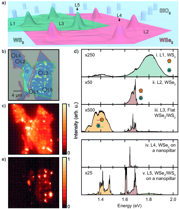
Figure 1a is an illustration of our device, fabricated by exfoliating WSe2 and WS2 monolayers from bulk crystals and transferring these onto a SiO2/Si substrate patterned with an array of nanopillars 220-250 nm tall and 4 m apart (see Methods and Section 1 of the Supplementary Information, SI). We choose an interlayer stacking angle of 50º, away from high-symmetry angles of 0º or 60º, in order to introduce an interlayer momentum mismatch to reduce the exciton recombination rate. Five distinct locations are labelled in Fig. 1a as L1-L5. These locations are marked by circles in the optical image of our device shown in Fig. 1b, where the WSe2 and WS2 monolayers are outlined in red and green, respectively, yielding a large region (160 m2) of the WS2/WSe2 heterobilayer.
Figure 1c shows a photoluminescence (PL) map taken with continuous-wave (CW) 2.33-eV (532-nm) laser excitation at a temperature T=4 K. This energy is greater than both the WSe2 and WS2 optical bandgaps of 1.73 eVJones2013 and 2.08 eVMitioglu2013 , respectively. Consequently, PL emission is observed from both monolayer and heterobilayer regions. The spectral emission from the flat monolayer regions (L1 and L2 in Fig. 1b) is shown in Figs. 1d (i) and (ii), respectively. The PL emission between 1.65 and 2.0 eV in panel (i) (filled in green) is the intralayer exciton recombination in monolayer WS2Mitioglu2013 ; Palacios2017 , and that between 1.6 and 1.75 eV in panel (ii) (filled in red) is the intralayer exciton recombination in monolayer WSe2Jones2013 ; Barbone2018 . Figure 1d panel (iii) shows the spectrum from the flat part of the heterobilayer, L3 in Fig. 1b. A lower-energy feature around 1.4 eV (filled in yellow) is consistent with interlayer exciton emission from stacked WS2/WSe2 heterobilayers reported previouslyJin2019 ; Jin2019b . Figure 1d (iv) is the PL spectrum from a monolayer WSe2 on a nanopillar, presented as reference, displaying a 50-fold brighter emission with respect to flat monolayer WSe2 and a sub-meV full-width at half-maximum spectral peak. Given that monolayer WSe2 on such nanopillars results in the strong quantum confinement of intralayer excitonsPalacios2017 ; Branny2017 , we look for similar signatures in the interlayer emission spectra. Figure 1d (v) is the PL spectrum of the heterobilayer on a nanopillar. We observe a 20-fold brighter interlayer emission in the low optical excitation regime (below 1 W) and sharp spectral features (1 meV full-width at half-maximum), in contrast to the weak and spectrally broad emission from the flat heterobilayer.
To isolate interlayer excitations from any effects coming from the monolayers, such as free charge carriers or intralayer excitons, we use an optical excitation energy of 1.50 eV for all other measurements. This energy is at the onset of the interlayer exciton PL spectrum, Fig. 1d (iii), and below the optical bandgap energies of WSe2 and WS2 monolayers. Figure 1e displays the PL intensity map of our device under 1.50-eV excitation. The emission is only observed from the heterobilayer region with both monolayer regions remaining dark, demonstrating that only interlayer excitons are generated, as anticipated.
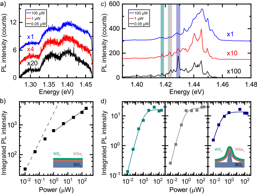
Figure 2a shows the interlayer exciton PL spectra from the flat heterobilayer for 0.05-W (black curve), 1-W (red curve) and 100-W (blue curve) laser excitation power, P, at T=4 K. The spectrally integrated PL intensity of interlayer exciton with respect to P is shown in Fig. 2b. While the interlayer exciton emission starts with a linear dependence on P, it converges to a P0.3 scaling for P0.3 W. Sublinear behaviour was also reported for MoSe2/WSe2 heterobilayersRivera2015 . This can be caused by density-dependent mechanisms such as exciton-exciton annihilation, dipolar repulsion and phase-space filling.
Figure 2c presents PL spectra from the heterobilayer on a nanopillar for P=0.05 W (black curve), 1 W (red curve) and 100 W (blue curve). With increasing power the three peaks highlighted in green, grey and blue saturate. The integrated PL intensity as a function of P from these peaks are plotted in Fig. 2d, with data (squares) colour-coded for the highlighted peaks of Fig. 2c. Each shows a linear P-dependence, followed by saturation. This behaviour is characteristic of a quantum-confined systemKurtsiefer2000 ; He2015 , and contrasts that of untrapped interlayer excitons in the flat heterobilayer (Figs. 2a and b). Eight nanopillar locations display this saturating behaviour (Fig. S3a in SI), demonstrating that interlayer-exciton trapping is reproduced across the device.
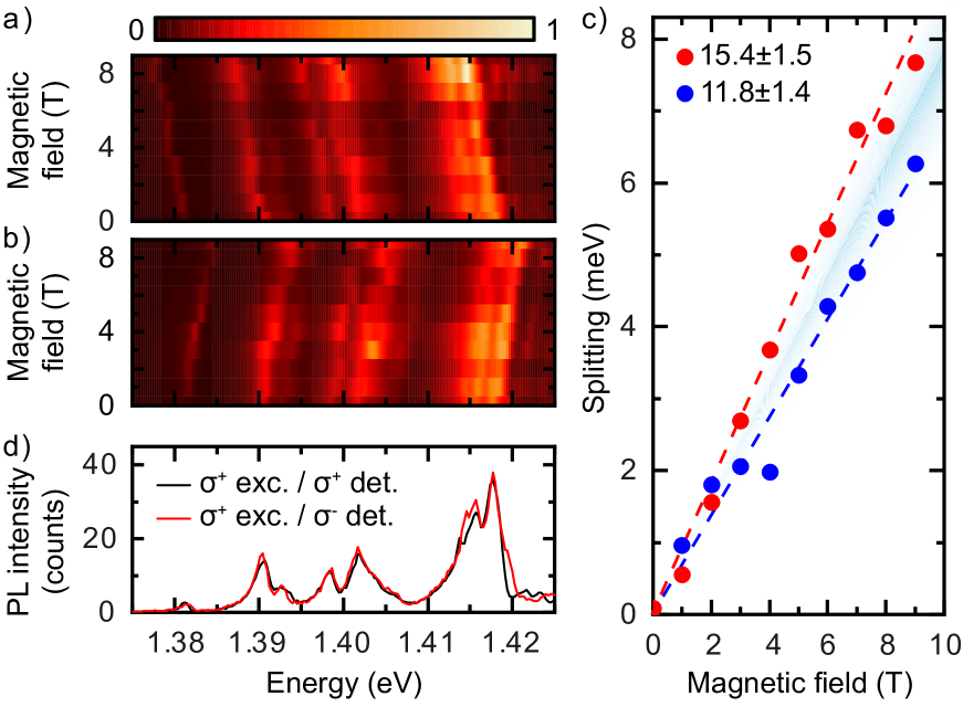
Figures 3a and 3b present trapped interlayer exciton PL spectra above a nanopillar (L5 of Fig. 1b) at T=4 K, for out-of-plane magnetic field B from 0 to 9 T. In panel a (panel b) the excitation is linearly polarised and the collection is right-hand (left-hand ) circularly polarised. The red-shifting Zeeman state from each emission line is only seen for detection, while the blue-shifting Zeeman state is only seen for detection. This demonstrates that the two magnetic configurations of trapped interlayer excitons have sustained optical selection rulesAivazian2015 .
The distribution of Zeeman splitting with respect to B across different nanopillars is given in Fig. 3c as a blue-shaded region, where the data corresponding to the smallest and largest measured g-factor (11.9 and 15.4) are plotted in blue and red circles, respectively. The similarity in g-factors, mean value 13.21.1, across the nanopillar traps and for different PL peaks (Fig. S3b in SI) suggests that the trapped excitons have the same microscopic origin. The variation in g-factors is also similar to that observed in confined intralayer excitons in WSe2 monolayersSrivastava2015 ; He2015 ; Koperski2015 ; Chakraborty2015 . This contrasts the order of magnitude smaller distribution in g-factor observed for trapped interlayer excitons in homogeneous moiré trapping potentialsSeyler2019 .
Figure 3d presents the PL spectra under excitation at B=0 T for (black) and (red) circularly polarised collection. The overlap of the two spectra demonstrates that excitation polarisation is not maintained for trapped interlayer excitons. One dominant mechanism for this loss of polarisation is the exchange interaction between bound electron and holesGlazov2014 . For trapped interlayer excitons the exchange interaction rate and the exciton decay rate should be reduced proportionally with the increased electron-hole separation, but the exciton decay rate is additionally suppressed when the momentum-space overlap is reduced, as expected for heterobilayers with a stacking angle not matching 0º or 60ºNayak2017 .
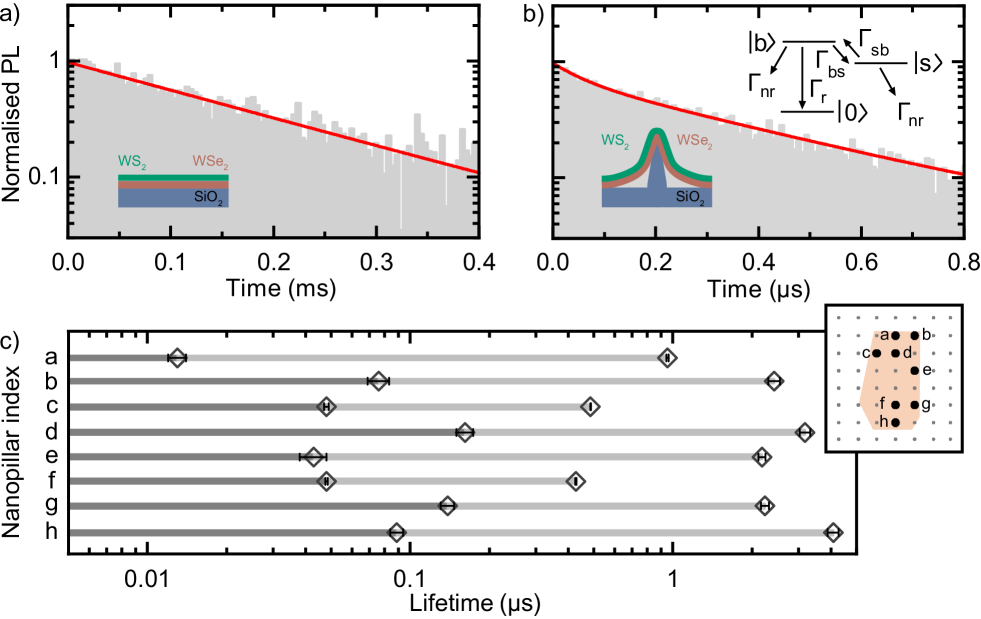
Figure 4 presents lifetime measurements on interlayer excitons under pulsed (3-ps pulse duration) laser excitation at 1.50 eV at T=4 K (see Methods). Figure 4a shows an example emission intensity histogram of untrapped interlayer excitons (grey bars) as a function of time after excitation, and an exponential fit (solid red curve) reveals a decay time of 180.63.5 s. Across the flat heterobilayer region, the average lifetime is 1755 s. Since only interlayer excitons are created under 1.50 eV excitation, spuriously prolonged lifetimes resulting from the delayed capture of free carriersShamirzaev2004 or higher energy intralayer dark excitonsJiang2018 are avoided. The spatial and momentum separation of electrons and holes of interlayer excitons, and the use of high-quality monolayers (see Methods), are likely responsible for these values. That said, this lifetime shows a strong excitation dependence: increasing the excitation power reduces the exciton decay time (Fig. S4 in SI), as expected from density-dependent interactions and loss channels, even in the regime where PL intensity depends linearly on the excitation power (P0.3 W in Fig. 2b).
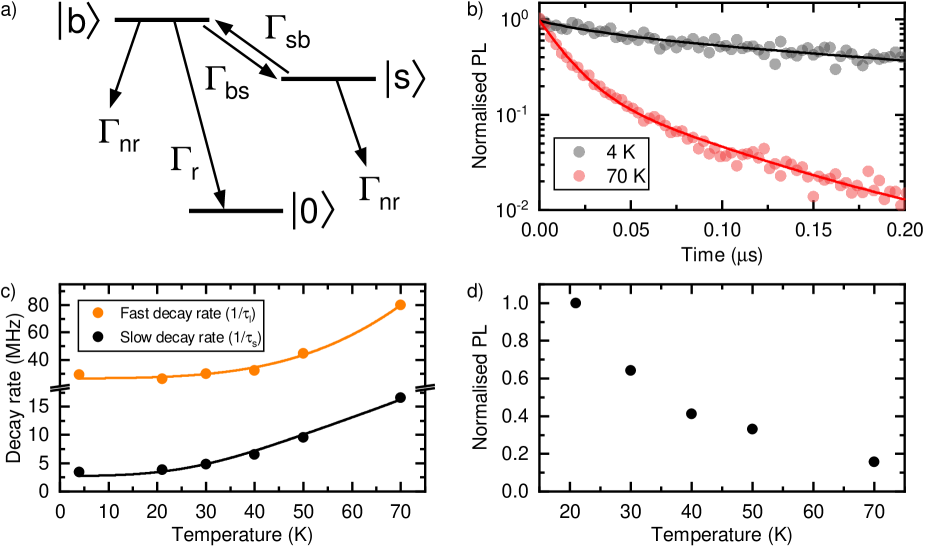
Figure 4b is a lifetime measurement of the trapped interlayer exciton spectral line at 1.39 eV from Fig. 3d (L5 in Fig. 1b). We fit a biexponential function of the form Ase+Ale, where () is the long (short) lifetime and () is the amplitude of the exponential with long (short) lifetime. This yields 59.40.9 ns and 389.11.2 ns. This biexponential behaviour, albeit with varying lifetimes, is observed throughout the entire spectral range for trapped interlayer excitons (Fig. S5 in SI). Figure 4c is a summary of the spectrally integrated lifetimes from the eight nanopillar traps. The extracted and values are shown in Fig. 4c in black and grey bars, and lie in the 10-175 ns and 0.4-4 s ranges, respectively. The reduction in the interlayer exciton lifetime after trapping accompanies an enhancement in PL brightness, suggesting a modified oscillator strength under localisation. This likely arises from the relaxation of stacking-angle-induced momentum mismatch on nanopillars, that otherwise inhibits the recombination of untrapped interlayer excitonsFeierabend2017 . One possible origin of the observed biexponential decay is the presence of two excited states: an optically active state and an energetically similar shelving state (inset diagram in Fig. 4b). A three-level model combined with temperature-dependent measurements (Section 5 in SI) yields average radiative and non-radiative recombination rates of trapped interlayer excitons across the nanopillar sites 13 MHz and 500 kHz, respectively. This reveals the considerably smaller average non-radiative decay rate and indicates that the long-lived shelving state decays primarily through radiative emission. Temperature-dependent measurements demonstrate that thermal excitations also couple bright and shelving states as evidenced in Fig. S6d of SI.
The spatial trapping we show here is a first step towards building arrays of long-lived and interacting interlayer excitons. Our trapped interlayer exciton lifetime, 4 s, is sufficient to observe dipole-mediated exciton interactions for an optically resolvable lattice spacing of 0.5 m. The immediate next step is to develop a full account of the photophysics of these trapped interlayer excitons, including the influence of stacking angle, interlayer spacing, electrostatic gating of the heterobilayer, and resonant excitation. In addition, other trapping geometries, such as ridges and rings, can offer the opportunity to probe many-body phenomena in one dimension.
I Acknowledgements
We acknowledge funding from the EU Quantum Technology (2D-SIPC) and Graphene Flagships; ERC grants PEGASOS, Hetero2D and GSYNCOR; EPSRC Grants EP/K01711X/1, EP/K017144/1, EP/N010345/1 and EP/L016057/1; and the Faraday Institution FIRG001. D. M. K. acknowledges support of a Royal Society university research fellowship URF\R1\180593. S.T. acknowledges support from DOE, NSF DMR 1552220, DMR 1904716, and NSF CMMI 1933214.
II Methods
II.1 Fabrication
Van der Waals TMD bulk crystals were synthesised through flux zone growth techniqueZhang2015 . Precursor powders were purchased from commercial vendors (Alfa Aesar) but additional electrolytic purification process was implemented to achieve 99.9999% or higher purity. After the purification these powders were analysed using secondary ion mass spectroscopy to confirm absence of metal impurities. Compared to crystals grown by chemical vapour transport, flux grown ones were free of point defects and topological defects.
Flakes are then prepared by micromechanical cleavageNovoselov2005 on Nitto Denko tape, then exfoliated again for transfer to a polydimethylsiloxane (PDMS) stamp placed on a transparent glass slide, allowing bidirectional inspection of the flakes under the optical microscope. Optical contrast is utilized to identify monolayers prior to transferCasiraghi2007 . We get monolayer flakes with lateral dimensions 50 m. Substrates with arrays of silica nanopillars, 100 nm in diameter and 220-250 nm high are prepared by direct-write lithographyPalacios2017 . The substrates undergo wet cleaning (1-minute ultrasonication in acetone and isopropanol) and are subsequently exposed to an oxygen-assisted plasma at a power of 10 W for 60 s to remove impurities and contaminants from the surface. The WSe2 monolayer is then stamped on the nanopillars with a micro-manipulator Palacios2017 ; Purdie2019 . After the first transfer, the second (WS2) monolayer is deposited on top of the WSe2 monolayer following the same stamping procedure. In both steps the PDMS stamp is removed after depositing the monolayer. Raman (Fig. S1a in SI), second-harmonic generation (Fig. S1b in SI) and atomic force microscopy (Fig. S2 in SI) measurements confirm the monolayer nature of the constituents, the twist angle and the interlayer spacing, respectively.
II.2 Photoluminescence measurements
All PL measurements are done at T=4 K in a 9-T closed-cycle cryostat (Attocube). Excitation and collection pass through a home-built confocal setup with the sample in reflection geometry. CW illumination from either a 2.33 eV laser (Ventus) or a Ti:Sapphire laser (Mira 900) at 1.58 or 1.50 eV is used. The PL signal is spectrally filtered and sent to a 150-line grating spectrometer (Princeton Instruments).
II.3 Lifetime measurements
To perform lifetime measurements, we excite the samples every few s (up to 10 s for the trapped interlayer excitons, and up to 1 ms for the interlayer exciton) with 3 ps pulses from a Ti:Sapphire laser (Mira 900) tuned to 785 nm (1.58 eV) or 825 nm (1.50 eV). An acousto-optic modulator (AOM) down-samples the 76 MHz laser repetition rate to the kHz-MHz range required to measure up to hundreds of s lifetimes. A time-to-digital converter (QuTau) with 81 ps timing resolution collects start-stop histograms with ”start” triggered by the AOM pulse-picking and ”stop” triggered by an avalanche photodiode (APD) output from single-photon detection of interlayer exciton PL. The converter remains idle until a subsequent ”start” signal arrives. We ensure that we are not susceptible to spurious artefacts from start-stop measurements by measuring lifetime at a subset of locations using photon time-tagging and calculating lifetimes in post-processing. Both methods result in consistent lifetimes for trapped interlayer excitons, but time-tagging is required for the measurement of the unbound interlayer exciton lifetimes, due to its count rate being comparable to or even lower than the APD dark counts, as well as being at least one order of magnitude smaller than the pulse rate sent to the sample.
References
- (1) Anderson, M. H. et al. Observation of Bose-Einstein Condensation in a Dilute Atomic Vapor. Science 269, 198–201 (1995).
- (2) Davis, K. B. et al. Bose-Einstein Condensation in a Gas of Sodium Atoms. Phys. Rev. Lett. 75, 3969–3973 (1995).
- (3) Greiner, M. et al. Quantum phase transition from a superfluid to a Mott insulator in a gas of ultracold atoms. Nature 415, 39 (2002).
- (4) Zwierlein, M. W. et al. Vortices and superfluidity in a strongly interacting Fermi gas. Nature 435, 1047–1051 (2005).
- (5) Schreiber, M. et al. Observation of many-body localization of interacting fermions in a quasirandom optical lattice. Science 349, 842-845 (2015).
- (6) Deng, H. et al. Condensation of semiconductor microcavity exciton polaritons. Science 298, 199–202 (2002).
- (7) Kasprzak, J. et al. Bose-Einstein condensation of exciton polaritons. Nature 443, 409–14 (2006).
- (8) Balili, R. et al. Bose-Einstein condensation of microcavity polaritons in a trap. Science 316, 1007–1010 (2007).
- (9) Plumhof, J. D. et al. Room-temperature Bose-Einstein condensation of cavity exciton-polaritons in a polymer. Nat. Mater. 13, 247 (2013).
- (10) Byrnes, T. et al. Exciton-polariton condensates. Nat. Phys. 10, 803 (2014).
- (11) Wertz, E. et al. Spontaneous formation and optical manipulation of extended polariton condensates. Nat. Phys. 6, 860 (2010).
- (12) Amo, A. et al. Superfluidity of polaritons in semiconductor microcavities. Nat. Phys. 5, 805 (2009).
- (13) Baranov, M. A. et al. Condensed matter theory of dipolar quantum gases. Chem. Rev. 112, 5012–5061 (2012).
- (14) Trefzger, C. et al. Ultracold dipolar gases in optical lattices. J. Phys. B: At. Mol. Opt. Phys. 44, 193001 (2011).
- (15) Lahaye, T. et al. The physics of dipolar bosonic quantum gases. Rep. Prog. Phys. 72, 126401 (2009).
- (16) Schauss, P. et al. Observation of spatially ordered structures in a two-dimensional Rydberg gas. Nature 491, 87 (2012).
- (17) Schauss, P. et al. Crystallization in Ising quantum magnets. Science 347, 1455 (2015).
- (18) Saffman, M. et al. Quantum information with Rydberg atoms. Rev. Mod. Phys. 82, 2313 (2010).
- (19) Truppe, S. et al. Molecules cooled below the Doppler limit. Nat. Phys. 13, 1173 (2017).
- (20) Bohn, J. L. et al. Cold molecules: Progress in quantum engineering of chemistry and quantum matter. Science 357, 1002 (2017).
- (21) Carr, L. D. Cold and ultracold molecules: science, technology and applications. New J. Phys. 11, 055049 (2009).
- (22) Griesmaier, A. et al. Bose-Einstein Condensation of Chromium. Phys. Rev. Lett. 94, 160401 (2005).
- (23) Lu, M. et al. Strongly Dipolar Bose-Einstein Condensate of Dysprosium. Phys. Rev. Lett. 107, 190401 (2011).
- (24) Aikawa, K. et al. Bose-Einstein Condensation of Erbium. Phys. Rev. Lett. 108, 210401 (2012).
- (25) Baier, S. et al. Extended Bose-Hubbard models with ultracold magnetic atoms. Science 352, 201 (2016).
- (26) de Paz, A. et al. Nonequilibrium Quantum Magnetism in a Dipolar Lattice Gas. Phys. Rev. Lett. 111, 185305 (2013).
- (27) Chen, Y. J. et al. Effect of electric fields on excitons in a coupled double-quantum-well structure. Phys. Rev. B 36, 4562 (1987).
- (28) Golub, J. E. et al. Type I–type II anticrossing and enhanced Stark effect in asymmetric coupled quantum wells. Appl. Phys. Lett. 53, 2584 (1988).
- (29) Voros, Z. et al. Long-Distance Diffusion of Excitons in Double Quantum Well Structures. Phys. Rev. Lett. 94, 226401 (2005).
- (30) Hubert, C. et al. Attractive Dipolar Coupling between Stacked Exciton Fluids. Phys. Rev. X 9, 021026 (2019).
- (31) Hubert, C. et al. Attractive interactions, molecular complexes, and polarons in coupled dipolar exciton fluids. arXiv:1910.06015 (2019).
- (32) Butov, L. V. et al. Macroscopically ordered state in an exciton system. Nature 418, 751 (2002).
- (33) High, A. A. et al. et al. Spontaneous coherence in a cold exciton gas. Nature 483, 584–588 (2012).
- (34) Shilo, Y. et al. Particle correlations and evidence for dark state condensation in a cold dipolar exciton fluid. Nat. Commun. 4, 2335 (2013).
- (35) Stern, M. et al. Exciton liquid in coupled quantum wells. Science 343, 55 (2014).
- (36) Rivera, P. et al. Observation of long-lived interlayer excitons in monolayer MoSe2-WSe2 heterostructures. Nat. Commun. 6, 6242 (2015).
- (37) Miller, B. et al. Long-Lived Direct and Indirect Interlayer Excitons in van der Waals Heterostructures. Nano Lett 17, 5229 (2017).
- (38) Rivera, P. et al. Interlayer valley excitons in heterobilayers of transition metal dichalcogenides. Nat. Nanotechnol. 13, 1004–1015 (2018).
- (39) Forg, M. et al. Cavity-control of interlayer excitons in van der Waals heterostructures. Nat. Commun. 10, 3697 (2019).
- (40) Jauregui, L. A. et al. Electrical control of interlayer exciton dynamics in atomically thin heterostructures. Science 366, 870 (2019).
- (41) Wang, G. et al. Colloquium: Excitons in atomically thin transition metal dichalcogenides. Rev. Mod. Phys. 90, 021001 (2018).
- (42) Kang, J. et al. Band offsets and heterostructures of two-dimensional semiconductors. Appl. Phys. Lett 102, 012111 (2013).
- (43) Gong, C et al. Band alignment of two-dimensional transition metal dichalcogenides: Application in tunnel field effect transistors. Appl. Phys. Lett. 103, 053513 (2013).
- (44) Fang, H. et al. Strong interlayer coupling in van der Waals heterostructures built from single-layer chalcogenides. Proc. Natl. Acad. Sci. U.S.A. 111, 6198 (2014).
- (45) Heo, H. et al. Interlayer orientation-dependent light absorption and emission in monolayer semiconductor stacks. Nat. Commun. 6, 7372 (2015).
- (46) Alexeev, E. M. et al. Resonantly hybridized excitons in moiré superlattices in van der Waals heterostructures. Nature 567, 81–86 (2019).
- (47) Tran, K. et al. Evidence for moiré excitons in van der Waals heterostructures. Nature 567, 71–75 (2019).
- (48) Nayak, P. K. et al. Probing Evolution of Twist-Angle-Dependent Interlayer Excitons in MoSe2/WSe2 van der Waals Heterostructures. ACS Nano 11, 4041-4050 (2017).
- (49) Seyler, K. L. et al. Signatures of moiré-trapped valley excitons in MoSe2/WSe2 heterobilayers. Nature 567, 66–70 (2019).
- (50) Jin, C. et al. Observation of moiré excitons in WSe2/WS2 heterostructure superlattices. Nature 567, 76–80 (2019).
- (51) Wang, Z. et al. Evidence of high-temperature exciton condensation in two-dimensional atomic double layers. Nature 574, 76 (2019).
- (52) Tang, Y. et al. WSe2/WS moiré superlattices: a new Hubbard model simulator. arxiv:1910.08673 (2019).
- (53) Shimazaki, Y. et al. Moiré superlattice in a MoSe2/hBN/MoSe2 heterostructure: from coherent coupling of inter- and intra-layer excitons to correlated Mott-like states of electrons. arxiv:1910.13322 (2019).
- (54) Regan, E. C. et al. Optical detection of Mott and generalized Wigner crystal states in WSe2/WS2 moiré superlattices. arxiv:1910.09047 (2019).
- (55) Bakr, W. et al. A quantum gas microscope for detecting single atoms in a Hubbard-regime optical lattice. Nature 462, 74 (2009).
- (56) Sherson, J. F. et al. Single-atom-resolved fluorescence imaging of an atomic Mott insulator. Nature 467, 68 (2010).
- (57) Kremser, M. et al. Discrete Interactions between a few Interlayer Excitons Trapped at a MoSe2-WSe2 Heterointerface. arxiv.org:1907.08815 (2019).
- (58) Li, W. et al. Dipolar interactions between field-tuneable, localized emitters in van der Waals heterostructures. arxiv.org:1910.08139 (2019).
- (59) Blackmore, J. A. et al. Ultracold molecules for quantum simulation: rotational coherences in CaF and RbCs. Quantum Sci. Technol. 4, 014010 (2019).
- (60) Jones, A. M. et al. Optical generation of excitonic valley coherence in monolayer WSe2. Nat. Nanotechnol. 8, 634 (2013).
- (61) Mitioglu, A. A. et al. Optical manipulation of the exciton charge state in single-layer tungsten disulfide. Phys. Rev. B 88, 245403 (2013).
- (62) Palacios-Berraquero, C. et al. Large-scale quantum-emitter arrays in atomically thin semiconductors. Nat. Commun. 8, 15093 (2017).
- (63) Barbone, M. et al. Charge-tuneable biexciton complexes in monolayer WSe2. Nat. Commun. 9, 3721 (2018).
- (64) Jin, C. et al. Identification of spin, valley and moiré quasi-angular momentum of interlayer excitons. Nat. Phys. 15, 1140 (2019).
- (65) Branny, A. et al. Deterministic strain-induced arrays of quantum emitters in a two-dimensional semiconductor. Nat. Commun. 8, 15053 (2017).
- (66) Kurtsiefer, C. et al. Stable Solid-State Source of Single Photons. Phys. Rev. Lett. 85, 290 (2000).
- (67) He, Y.-M. et al. Single quantum emitters in monolayer semiconductors. Nat. Nanotechnol. 10, 497 (2015).
- (68) Aivazian, G. et al. Magnetic control of valley pseudospin in monolayer WSe2. Nat. Phys. 11, 148 (2015).
- (69) Koperski, M. et al. Orbital, spin and valley contributions to Zeeman splitting of excitonic resonances in MoSe2, WSe2 and WS2 Monolayers. 2D Mater. 6, 015001 (2019).
- (70) Srivastava, A. et al. Optically active quantum dots in monolayer WSe2. Nat. Nanotechnol. 10, 491 (2015).
- (71) Koperski, M. et al. Single photon emitters in exfoliated WSe2 structures. Nat. Nanotechnol. 10, 503 (2015).
- (72) Chakraborty, C. et al. Voltage-controlled quantum light from an atomically thin semiconductor. Nat. Nanotechnol. 10, 507 (2015).
- (73) Glazov, M. M. et al. Exciton fine structure and spin decoherence in monolayers of transition metal dichalcogenides. Phys. Rev. B, 89, 201302(R) (2014).
- (74) Shamirzaev, T. S. et al. Millisecond fluorescence in InAs quantum dots embedded in AlAs. Physica E Low Dimens. Syst. Nanostruct. 20, 282 (2004).
- (75) Jiang, C. et al. Microsecond dark-exciton valley polarization memory in two-dimensional heterostructures. Nat. Commun. 9, 1–8 (2018).
- (76) Feierabend, M. et al. Impact of strain in the optical fingerprint of monolayer transition-metal dichalcogenides. Phys. Rev. B, 96, 045425 (2017).
- (77) Zhang, X. et al. Flux method growth of bulk MoS2 single crystals and their application as a saturable absorber. Cryst. Eng. Commun. 17, 4026 (2015).
- (78) Novoselov, K. S. et al. Two-dimensional atomic crystals. Proc. Natl. Acad. Sci. U.S.A. 30, 10451 (2005).
- (79) Casiraghi, C. et al. Rayleigh Imaging of Graphene and Graphene Layers. Nano Lett. 7, 2711 (2007).
- (80) Purdie, D. G. et al. Cleaning interfaces in layered materials heterostructures. Nat. Commun. 9, 5387 (2018).
Supplementary information for
Confinement of long-lived interlayer excitons in WS2/WSe2 heterostructures
Alejandro R.-P. Montblanch,1,∗ Dhiren M. Kara,1,∗ Ioannis Paradisanos,2 Carola M. Purser,1,2 Matthew S. G. Feuer,1 Evgeny M. Alexeev,2,1 Lucio Stefan,1,3 Ying Qin,4 Mark Blei,4 Gang Wang,2 Alisson R. Cadore,2 Pawel Latawiec,5 Marko Lončcar,5 Sefaattin Tongay,4 Andrea C. Ferrari,2,†, and Mete Atatüre1,‡
1Cavendish Laboratory, University of Cambridge, 19 J. J. Thomson Ave., Cambridge, CB3 0HE, UK
2Cambridge Graphene Centre, University of Cambridge, 9 J. J. Thomson Ave., Cambridge, CB3 0FA, UK
3The Faraday Institution, Quad One, Becquerel Avenue, Harwell Campus, Didcot, OX11 0RA, UK
4School for Engineering of Matter, Transport and Energy, Arizona State University, Tempe, AZ, 85287, USA
5School of Engineering and Applied Science, Harvard University, Cambridge, MA, 02138, USA
CONTENTS
1. Characterisation of WS2/WSe2 heterobilayer device 19
2. Statistics of trapped interlayer excitons: power saturation and magnetic-field
dependence 20
3. Power dependence of untrapped interlayer-exciton lifetime 21
4. Spectrally selective lifetime measurements on a nanopillar 21
5. Temperature dependence of trapped interlayer-exciton lifetime 22
∗These authors contributed equally.
†acf26@cam.ac.uk
‡ma424@cam.ac.uk
1. Characterisation of WS2/WSe2 heterobilayer device
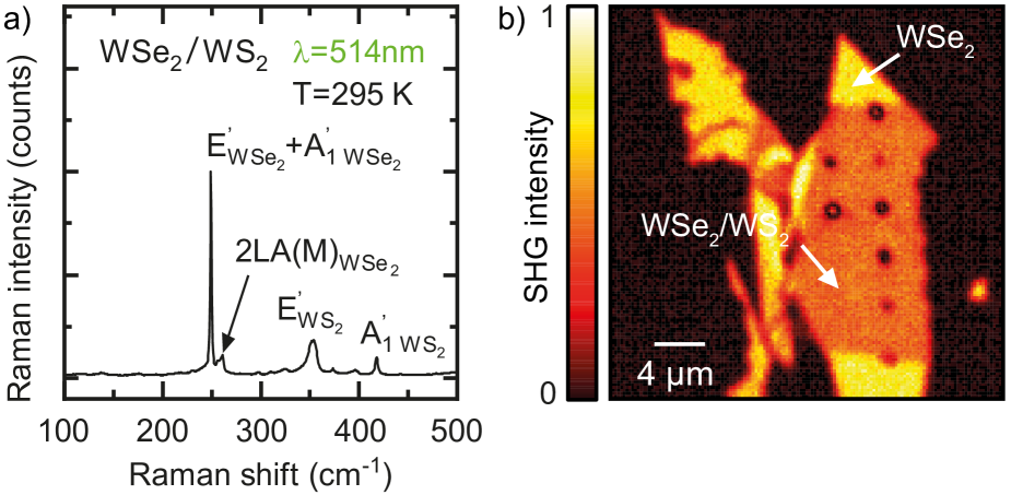
To characterise the sample structurally we perform room-temperature Raman measurements in a commercial Horiba LabRam Evolution system using a 514-nm laser at 60 W power. Figure S1a shows the Raman spectrum from the WS2/WSe2 heterobilayer on a flat region. The Raman peaks at 358 and 419 cm-1 correspond to the E and A modes of WS2, respectively[1]. The separation between them 61 cm-1 is consistent with it being monolayer[2]. The peak 251 cm-1, with full-width at half-maximum 2 cm-1, is assigned to the convoluted A+E modes of WSe2, degenerate in monolayer WSe2[1,2], while the peak 262 cm-1 belongs to the 2LA(M) mode of WSe2[1].
Figure S1b plots the spatially resolved map of the spectrally integrated second-harmonic signal from monolayer and heterobilayer regions. This is measured with a picosecond-pulsed Ti:Sapphire laser (3-ps pulse duration) at 76 MHz repetition rate and tuned to 982 nm at 1 mW CW-equivalent power. From the reduced intensity in the heterobilayer region compared to monolayer in Fig. S1b we infer a stacking angle between WSe2 and WS2 monolayers of 50º, closer to 60º because the stacking of the individual constituents close to that angle yield partial destructive interference resulting from the combination of the second harmonic signal from each individual monolayer[3]. This is confirmed by additional polarisation-resolved second-harmonic generation measurements at 1300-nm pump wavelength.
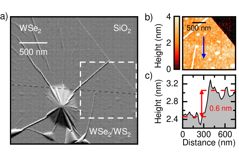
Figure S2a is the map of the amplitude retrace in the room-temperature atomic force microscope measurement (commercial head, model MFP- 3D from Asylum Research with silicon tips from Bruker) of an area of the device containing flat WSe2 monolayer and WS2/WSe2 heterobilayer regions, as well as WS2/WSe2 heterobilayer on top of a nanopillar. Figure S2b shows the topography of the area enclosed by the white dashed square in Fig. S2a. Figure S2c plots the height profile obtained averaging the line cuts spanning a length of 350 nm centered around the blue arrow of Fig. S2b, and shows that the step size from the WSe2 monolayer region to the WS2/WSe2 heterobilayer region coincides with the thickness of a monolayer, 0.6 nm[4].
2. Statistics of trapped interlayer excitons: power saturation and magnetic-field dependence
Figure S3a is a set of power saturation curves of trapped interlayer excitons measured on different nanopillar locations at a temperature T=4 K, showing that the saturation behaviour of trapped interlayer excitons is reproducibly found across the device. We fit the data to the saturation function
| (1) |
where P is the excitation power, A is the PL intensity at saturation, Psat is the saturation power, and n is the exponent that describes the power law followed by P at low excitation powers. We find a distribution of saturation powers with standard deviation 5 W, indicative of a range of slightly dissimilar confining potentials. This is also supported by the observed variation in trapped exciton g-factors and lifetimes (Figs. 3c and 4c in the main text). We find an average value of n=1.000.12. This linear dependence, reproduced across the device, suggests that the trapped interlayer excitons do not experience density-dependent decay mechanisms due to excitons around the nanopillar. This contrasts evidence of strong density dependence of the unbound interlayer excitons, which exhibits non-linear excitation-power dependence (Fig. 2b in the main text) as well as population-dependent lifetimes (Fig. S4).
Figure S3b plots the Zeeman splitting of trapped interlayer exciton emission in two example nanopillar locations. The solid curves are linear fits to the data, from which we extract the g-factors of the trapped interlayer excitons according to[5]:
| (2) |
where () is the emission energy of a trapped interlayer exciton with () collection, is the trapped interlayer exciton g-factor, eV T-1 is Bohr’s magneton and is the applied magnetic field. The g-factors obtained from the linear fits in Fig. S3b contribute to the Zeeman splitting distribution of similar g-factors with average value 13.21.1, as stated in the main text and represented in Fig. 3c by a blue-shaded area. The similarity in the g-factor distribution between both locations suggests that the magnetic states at each confining potential have the same microscopic origins, albeit not identical across a given nanopillar location.
3. Power dependence of untrapped interlayer-exciton lifetime
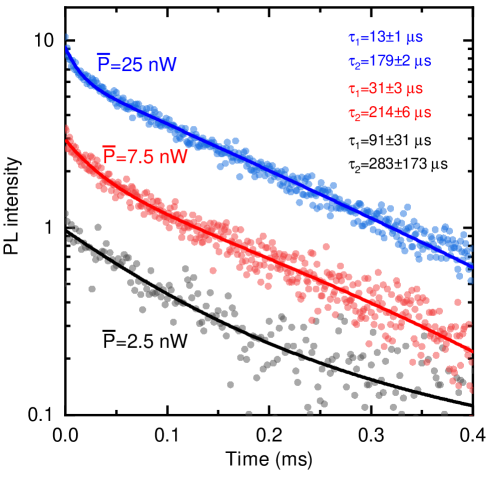
We measure the lifetime of the untrapped interlayer excitons as a function of average pump power, , at T=4 K. We adjust by gating the pulsed laser (76-MHz repetition rate / 13-ns pulse separation) with varying gate windows from 50 ns up to 500 ns for a fixed histogram range of 1 ms. Figure S4 are lifetime measurements for three in the linear pump power-PL intensity regime: nW (black filled circles), nW (red filled circles) and nW (blue filled circles). The two lifetimes and quoted in Fig. S4 for each measurement are extracted from biexponential fits (solid curves). We observe that at larger pump powers a biexponential fit is required (see for example the red curve), while at lower pump powers a monoexponential fit suffices (as evidenced by the large fit error of the lifetime taken with the lowest nW, black curve). This suggests a change in the dynamics of untrapped interlayer excitons with increasing pump powers. Additionally, in the linear excitation power regime, where the intensity scales linearly with , we observe a variation of both and . This contrasts the behaviour of a non-interacting system, where the measured lifetimes would remain constant. Thus, this measurement supports the existence of density-dependent dynamics of untrapped interlayer excitons, as was already discussed for Fig. 2c of the main text.
4. Spectrally selective lifetime measurements on a nanopillar
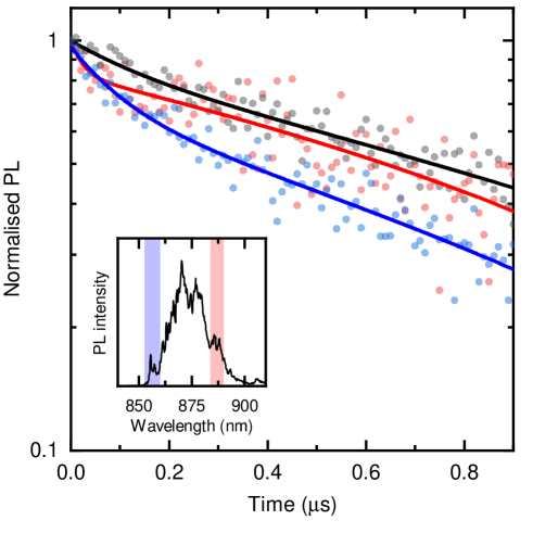
Figure S5 is a lifetime measurement on a nanopillar at T=4 K: the red (blue) dots corresponds to the red-shaded (blue-shaded) spectral region of the PL spectrum in the inset. The black dots are the lifetime measurement of the whole spectrum. We find that all measurements are best fit with a biexponential function (solid curves in Fig. S5), from which we extract 24.24.0 ns and 3.530.09 s (red), 104.6 2.7ns and 1.660.03 s (blue), and 159.98.8 ns and 3.000.10 s (black). Thus, the biexponential behaviour is maintained regardless of the selected spectral window, and is observed across all nanopillar locations.
While there is a slight variation, expected for distinct confining potentials across a nanopillar, lifetimes are within the same order of magnitude for different spectral regions and we do not capture any correlation between spectrum and lifetime. The biexponential is observed down to the single-peak level, as presented in the lifetime measurement in Fig. 4b of the spectrally isolated peak at 1.39 eV in Fig. 3d of the main text.
The close similarity between the lifetime of the spectrally selected regions and the lifetime extracted for the integrated PL spectrum, combined with the similarity in intensities among all spectral peaks for a given nanopillar, prevents the distinction of each individual biexponential decay for each single peak in a lifetime measurement of the integrated PL spectrum on a nanopillar. The measured lifetimes are thus representative of the average lifetimes for trapped interlayer excitons at each nanopillar location, and justifies our reporting of the average lifetime from each nanopillar location in Fig. 4c as extracted by collecting the PL from the entire, integrated PL spectrum.
5. Temperature dependence of trapped interlayer-exciton lifetime
To explain the biexponential decay of the trapped interlayer excitons we start with a three-level model, depicted in Fig. S6a, consisting of a bright state b, an optically inactive shelving state s and a ground state 0. Similar models have been used earlier in other systems with biexponential decay characteristics, such as self-assembled quantum dots[6] and carbon nanotubes[7].
The rate equations governing the populations and of the bright and shelving states in such a system are:
| (3) |
| (4) |
where the radiative rate for the bright state is , the coupling rates between the bright and the shelving states are (bright to shelving) and (shelving to bright), and the nonradiative decay rate for the bright and shelving states (assumed to be equal for simplicity) is .
Solving the system of linear differential Eqs. (3,4) yields a biexponential population decay in time for of the form Ase+Ale as written in the main text, with time constants given by
| (5) |
We identify the fast decay rate with the + sign of Eq. (5) and the slow decay rate with the - sign of Eq. (5).
We perform temperature-dependent lifetime measurements to elucidate the dominating rate and gain insight on the decay mechanisms. Figure S6b is an example lifetime measurements taken on a nanopillar at two different temperatures: 4 K (black filled circles) and 70 K (red filled circles). We extract, for an example nanopillar location, the two exponents of the biexponential fit at different temperatures, and present them as rates 1/ (fast decay rate) and 1/ (slow decay rate) in Fig. S6b as orange and black dots, respectively. We observe a strong dependence of both 1/ and 1/ with temperature, suggesting that , and (Fig. 4 in the main text) are thermally activated: a common mechanism for nonradiative processes, as well as coupling between a bright and a shelving state, is through phonon mediation. To model this coupling we assume a multi-phonon process involving a continuum phonon density of states[8] and set the temperature dependences for , and to be, respectively:
| (6) |
| (7) |
| (8) |
where is temperature, is the spontaneous non-radiative rate at 0 K, is the pre-factor of for , is the rate of population transfer from the bright to the shelved state at 0 K, is the pre-factor of for both and , and describes the power law scaling of with . depends on the exact phononic coupling mechanism[8], and we assume for simplicity to be the same for all . The solid curves in Fig. S6b are fits to the data obtained by substituting Eqs. (6-8) into Eq. (5), where is left as a constant in because it physically depends only on the optical dipole transition strength. We obtain 3, a value that has been obtained before in other quantum emitters[8] and confirms the strong temperature dependence of , and . The remaining fit values are: MHz, MHz, K-3, MHz and K-3.
With these values, has a meaningful contribution starting at 20 K, which corresponds to an energy of 2 meV, and becomes comparable in magnitude to at 40 K. Our model reveals that at low temperatures (below 20 K), when is small, Eq. (5) can be approximated as:
| (9) |
| (10) |
In this case, in the biexponential fit of a lifetime measurement becomes a direct measure of in the limit of low temperature. Because is more than one order of magnitude larger than in our measurements (Fig. 4c in the main text), is small compared at least to the sum indicating that, at low temperatures, the dynamics of trapped interlayer excitons is not limited by nonradiative processes. In particular, applying the fit parameters in Eqs. (6-8) we obtain, at 4 K, =20.1 MHz, =2.8 MHz and =3.8 MHz: is roughly one order of magnitude larger than and , so that is an approximate measure of in the limit of low temperature. We note that it is the long-lived shelving state that enables this relation: a model with only one excited state would yield a single exponential and not two. Additionally, the measured lifetimes up to 4 s (Fig. 4c in the main text) indeed indicate that a strong fraction of the trapped interlayer excitons will live for that long, regardless of the mechanism that enables this. At 4 K we find, from the values in Fig. 4c in the main text, that the average radiative rate across nanopillars is 13 MHz, and the average non-radiative rate is 500 kHz.
At temperatures beyond 40 K, when , the model becomes:
| (11) |
| (12) |
With our fit parameters we find, at 70 K, =20.1 MHz, =8.5 MHz, =31.2 MHz and =27.4 MHz, so that nonradiative processes and population transfer to (and from) the shelving state are at this temperature more relevant. Our model predicts the decrease in quantum efficiency with increasing temperature. Indeed, the thermally induced modification in the dynamics is evidenced in Fig. S6d: it plots the PL intensity of trapped interlayer excitons as a function of temperature, showing that as nonradiative processes are thermally activated, the PL intensity decreases.
Finally, we note that an exponential temperature dependence of the form (with the activation energy, the Boltzmann constant and temperature), used in other systems in the context of the Mott-Seitz model[9], also fits our data reasonably with similar parameter values. Thus, while the three-level model with temperature-dependent rates captures the trapped interlayer exciton dynamics successfully, a thorough theoretical study and further experimental analysis is necessary to understand the full microscopic nature of the system.
References
[1] Terrones, H. et al. New first order Raman-active modes in few layered transition metal dichalcogenides. Sci. Rep. 4, 4215 (2014).
[2] Zhao, W. et al. Lattice dynamics in mono- and few-layer sheets of WS2 and WSe2. Nanoscale 5, 9677 (2013).
[3] Hsu, W.-T. et al. Second Harmonic Generation from Artificially Stacked Transition Metal Dichalcogenide Twisted Bilayers. ACS Nano 8, 2951-2958 (2014).
[4] Rosenberger, M et al. Nano-”Squeegee” for the Creation of Clean 2D Material Interfaces. ACS Appl. Mater. Interfaces 10, 10379 (2018).
[5] Aivazian, G. et al. Magnetic control of valley pseudospin in monolayer WSe2. Nat. Phys. 11, 148 (2015).
[6] Tighineanu, P. et al. Decay dynamics and exciton localization in large GaAs quantum dots grown by droplet epitaxy. Phys. Rev. B 88, 155320 (2013).
[7] Berciaud, S. et al. Luminescence Decay and the Absorption Cross Section of Individual Single-Walled Carbon Nanotubes. Phys. Rev. Lett. 101, 077402 (2008).
[8] Jahnke, K. D. et al. Electron–phonon processes of the silicon-vacancy centre in diamond. New J. Phys. 17, 043011 (2015).
[9] Toyli, D. M. et al. Measurement and Control of Single Nitrogen-Vacancy Center Spins above 600 K. Phys. Rev. X 2, 031001 (2012).
