Electrical switching of magnetic order in an orbital Chern insulator
Magnetism typically arises from the joint effect of Fermi statistics and repulsive Coulomb interactions, which favors ground states with non-zero electron spin. As a result, controlling spin magnetism with electric fields—a longstanding technological goal in spintronics and multiferroicsMatsukura et al. (2015); Jiang et al. (2018)—can be achieved only indirectly. Here, we experimentally demonstrate direct electric field control of magnetic states in an orbital Chern insulatorSharpe et al. (2019); Serlin et al. (2020); Chen et al. (2020); Lu et al. (2019), a magnetic system in which non-trivial band topology favors long range order of orbital angular momentum but the spins are thought to remain disorderedXie and MacDonald (2020); Bultinck et al. (2020); Zhang et al. (2019a); Liu and Dai (2020); Wu and Das Sarma (2020); Chatterjee et al. (2020); Repellin et al. (2020); Alavirad and Sau (2019). We use van der Waals heterostructures consisting of a graphene monolayer rotationally faulted with respect to a Bernal-stacked bilayer to realize narrow and topologically nontrivial valley-projected moiré minibandsMa et al. (2019); Park et al. (2020); Rademaker et al. (2020). At fillings of one and three electrons per moiré unit cell within these bands, we observe quantized anomalous Hall effectsChang et al. (2013) with transverse resistance approximately equal to (where is Planck’s constant and is the charge on the electron), which is indicative of spontaneous polarization of the system into a single-valley-projected band with a Chern number equal to two. At a filling of three electrons per moiré unit cell, we find that the sign of the quantum anomalous Hall effect can be reversed via field-effect control of the chemical potential; moreover, this transition is hysteretic, which we use to demonstrate nonvolatile electric field induced reversal of the magnetic state. A theoretical analysisZhu et al. (2020) indicates that the effect arises from the topological edge states, which drive a change in sign of the magnetization and thus a reversal in the favored magnetic state. Voltage control of magnetic states can be used to electrically pattern nonvolatile magnetic domain structures hosting chiral edge states, with applications ranging from reconfigurable microwave circuit elements to ultralow power magnetic memory.
The quantized anomalous Hall effectHaldane (1988) occurs in two dimensional insulators whose filled bands have a finite net Chern number, and requires broken time-reversal symmetry. Chern bands arise naturally in graphene systems when the Dirac spectrum acquires a mass, for instance due to the breaking of sublattice symmetry in monolayer graphene by a hexagonal boron nitride substrateSong et al. (2015). Absent electron-electron interactions, bands located in the two inequivalent valleys at opposite corners of graphene’s hexagonal Brillouin zone are constrained by time reversal symmetry to acquire equal and opposite Chern numbers. In some graphene systems, a periodic moiré superlattice can be used to engineer superlattice bands which generically preserve the nonzero Chern numbers that arise from the incipient Berry curvature of the monolayer graphene Dirac pointsZhang et al. (2019b); Liu et al. (2019a). When the bandwidth of the superlattice bands is sufficiently small, the importance of electron-electron interactions is enhanced leading to symmetry breaking that manifests primarily as resistivity peaks at integer filling of normally four-fold degenerate superlattice bandsBistritzer and MacDonald (2011); Cao et al. (2018); Chen et al. (2019). Among the states potentially favored by interactions are those with spontaneous breaking of time reversal symmetryBultinck et al. (2020); Zhang et al. (2019a); Liu and Dai (2020); Wu and Das Sarma (2020); Chatterjee et al. (2020); Repellin et al. (2020); Alavirad and Sau (2019), and indeed ferromagnetism and quantum anomalous Hall effects have been observed in both twisted bilayer graphene aligned to hexagonal boron nitrideSharpe et al. (2019); Serlin et al. (2020) and rhombohedral trilayer graphene, also aligned to hexagonal boron nitrideChen et al. (2020). In contrast to quantum anomalous Hall effects observed in magnetically doped topological insulators which are spin ferromagnets rendered strongly anisotropic by their large spin orbit coupling, in graphene moiré systems the spin orbit coupling vanishes and the magnetism is thought to be primarily orbital, leading these systems to be dubbed ‘orbital Chern insulators’.
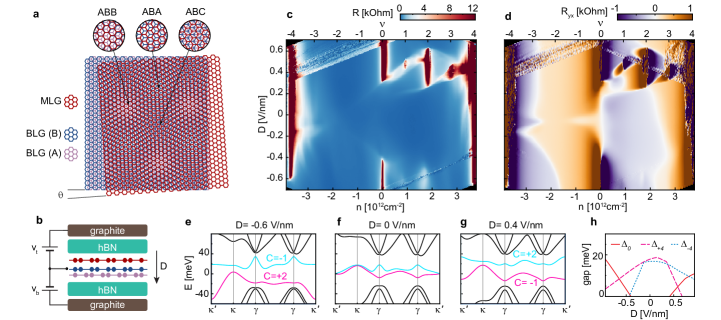
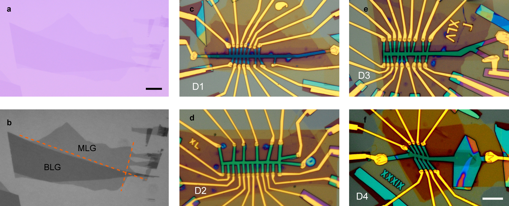
Here we introduce another moiré heterostructure that shows quantum anomalous Hall effects. As shown in Figure 1a, our devices consist of a graphene monolayer rotationally faulted with respect to a Bernal stacked graphene bilayer, which we refer to as twisted monolayer-bilayer graphene (tMBG). The tMBG moiré consists of a triangular lattice of ABB-stacked regions interspersed with more structurally stable ABA and ABC regions, as illustrated in Figure 1a; in the low energy bands, wave functions are localized near the ABB regions. Our devices are fabricated by applying a ‘cut-and-stack’ method to an exfoliated graphene flake that contains both monolayer and bilayer graphene regions (see Methods and Extended Data Fig. E1). Two graphite gates above and below the tMBG layer allow independent control of the overall carrier density and electric displacement field, , where is the vacuum permittivity, is the applied voltage and is the capacitance per unit area of the top (bottom) gate (see Figure 1b).
D-field tunable flat bands
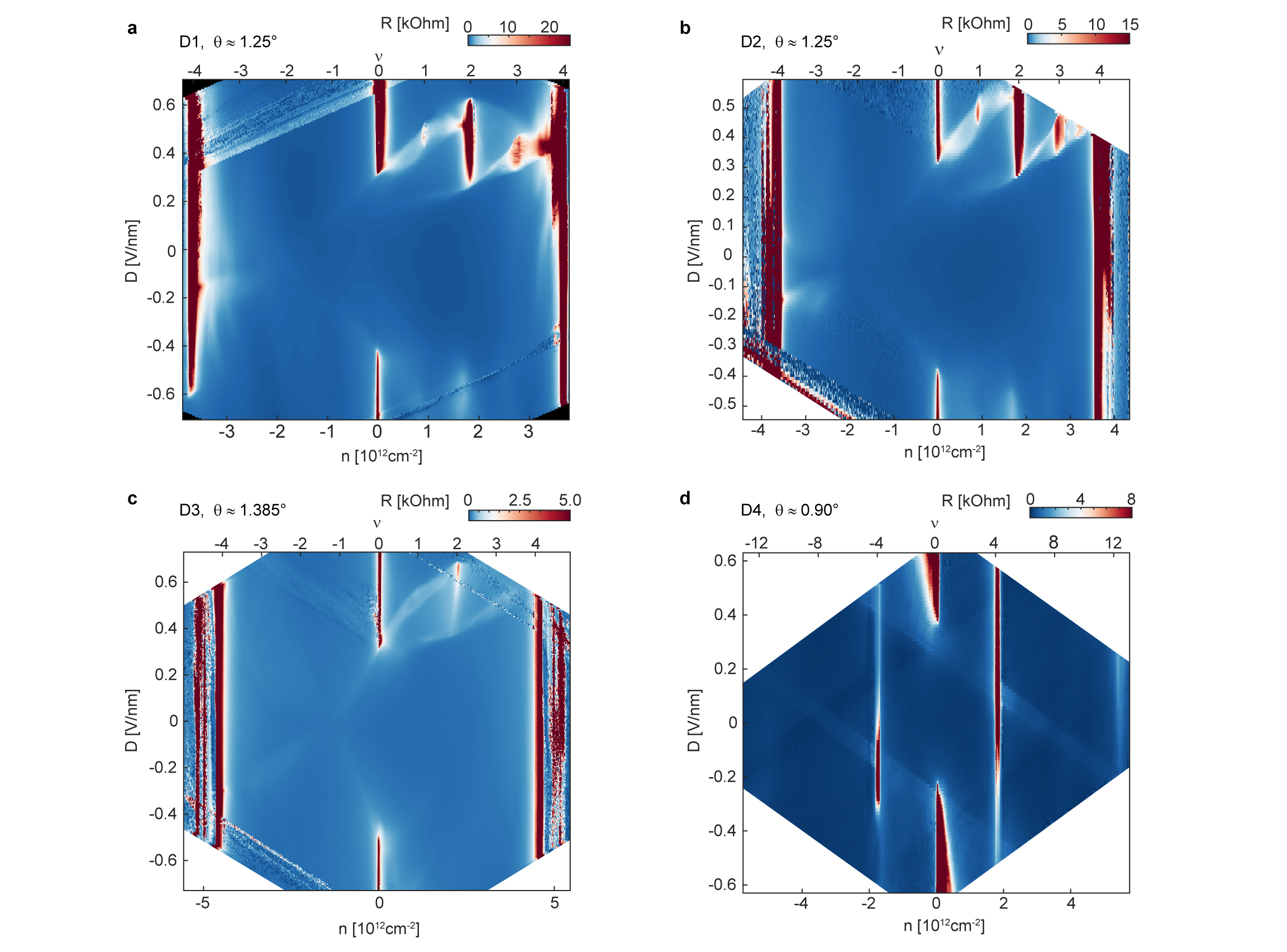
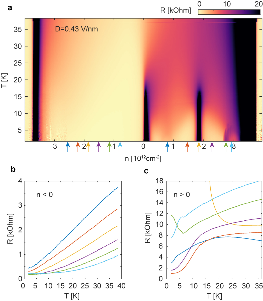
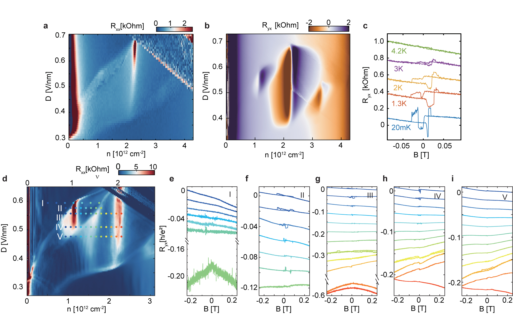
Figs. 1c-d show longitudinal and Hall resistance as a function of and for a device with interlayer twist angle . Additional data from devices with a range of twist angles between 0.9 and 1.4∘ are shown in Extended Data Fig. E2. All devices show resistance peaks at , where denotes the number of carriers per superlattice unit cell, is the unit cell area and Å is the lattice constant of graphene. Correlated states, revealed by sign changes in the Hall resistance and peaks in the longitudinal resistance are observed near and for devices with and . They appear only within a narrow range of displacement fields near V/nm, with onset temperatures as high as 20 K (Figure E3). In all such devices an anomalous Hall effect is observed at and , as shown in E4 and E5.
Similar observations in rotationally faulted bilayer-bilayer grapheneShen et al. (2020); Liu et al. (2019b); Cao et al. (2020); Burg et al. (2019); He et al. (2020) have been interpreted as arising from displacement field tuned formation of an isolated narrow band, and consequent spontaneous breaking of spin, valley, or lattice symmetries that result in correlated insulating states at integer fillings. A previous theoretical studyMa et al. (2019) has suggested that tMBG similarly hosts narrow electronic bands at small twist angles around . In our data, the domains of displacement field over which correlated physics is observed aligns with where numerical simulations (Figure 1e-h) show the formation of a narrow, isolated band. The electronic band structure of tMBG arises from the moiré-induced hybridization of the monolayer graphene Dirac cone (located at the point in the band structure diagrams of Figs. 1e-g) with the parabolic low energy band of the bilayer (at the point). When the displacement field , low-energy valence and conduction bands are isolated from the other bands but overlap with each other, giving rise to gaps at but not at . At intermediate values of a gap opens at charge neutrality leading to the formation of isolated conduction and valence bands with nonzero Chern number. Further increase of then leads to band overlap between the low energy bands and higher energy dispersive bands. Correlated states at integer filling, accompanied by ‘halos’ of changed resistance relative to the background at non-integer filling, appear in the intermediate regime where both calculations (Figure 1h) and experimental data indicate the formation of a narrow and isolated conduction band.
Quantum anomalous Hall states with C=2
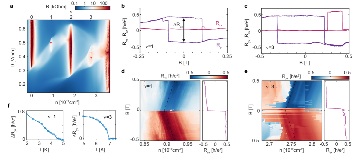
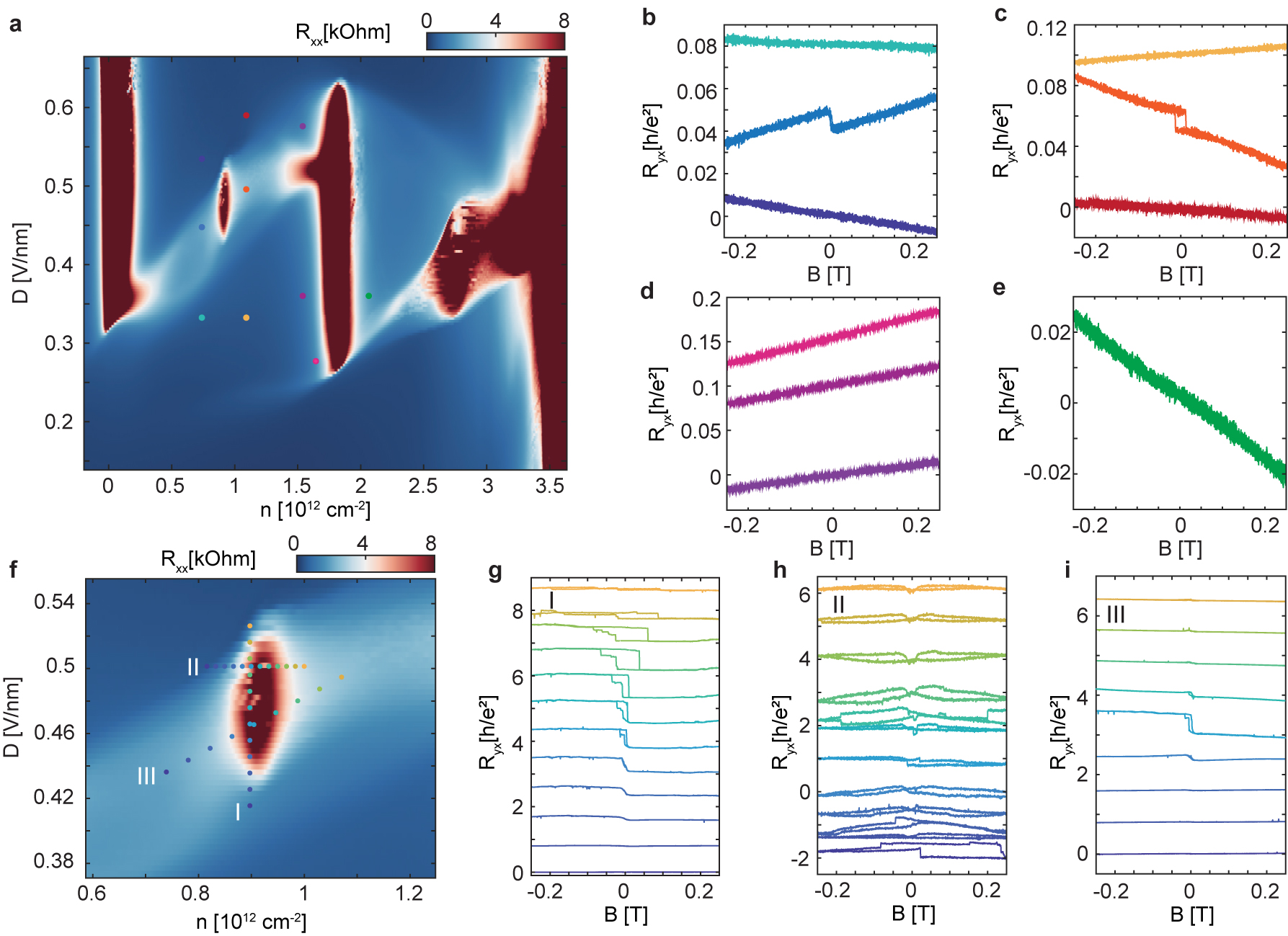
We focus on the , narrow-band regime, a detail of which is shown in Figure 2a. At , we observe a robust insulator, consistent with a topologically trivial gap. At both and , however, the resistance at B=0 is both noisy and comparatively low. Magnetoresistance measurements (Figs. 2b-c) reveal that the noise is due to magnetic hysteresis. In both cases, we observe rapid switching between states with , accompanied by a low . The saturation of the Hall resistance near is suggestive of polarization into bands with Chern number 2. The quantization is not precise, reaching only 85% of the expected value at , for instance. However, the evolution of the Hall plateau in magnetic field, shown in Figs. 2d-e, provides further evidence of an underlying orbital Chern insulator state. For both and 3, increasing the magnetic field shifts the center of the plateau in density (), in agreement with the Středa formulaStreda (1982), , which is applicable to any incompressible Chern insulator. Chern 2 bands were previously predictedMa et al. (2019) and are consistent with our own band structure calculation, which indicated that the conduction band has C=2 for a positive field.
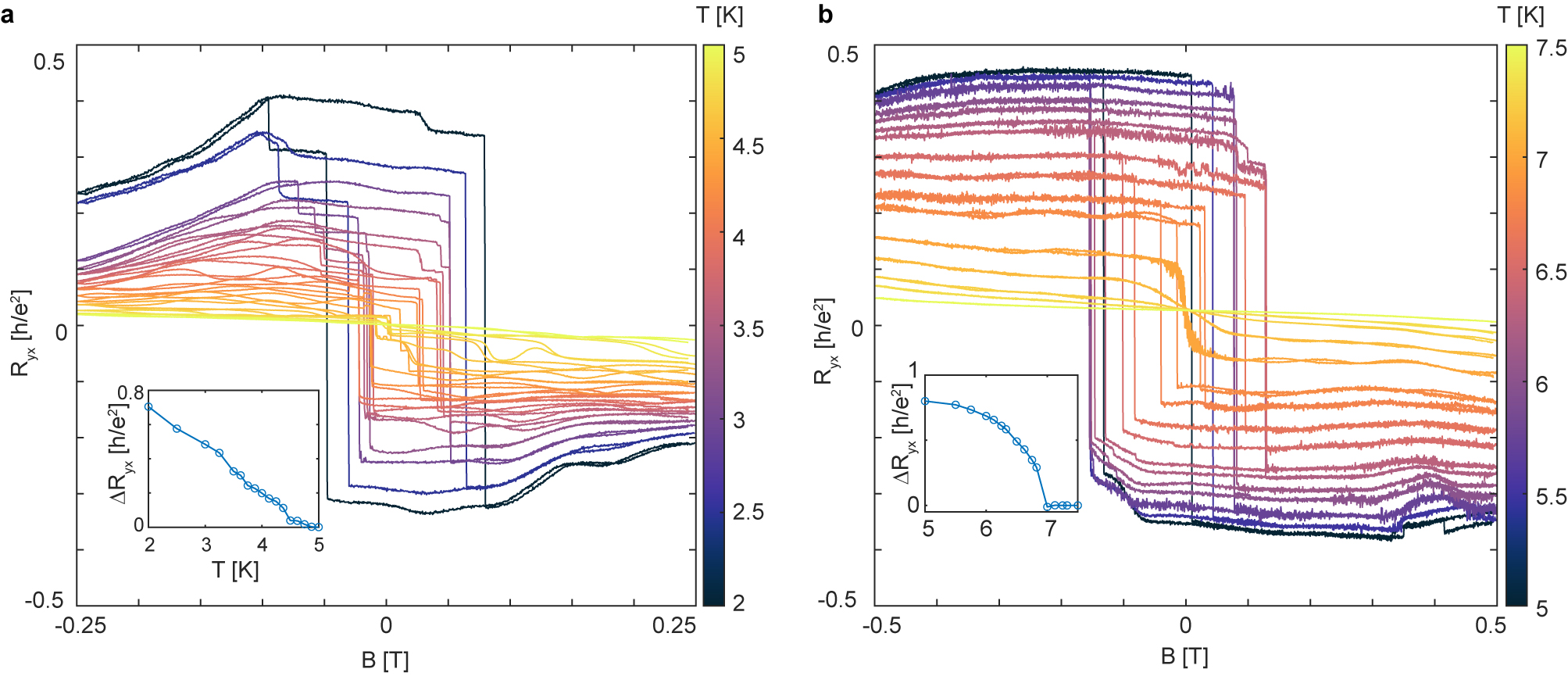
It is notable that tMBG, in contrast to both rhombohedral trilayer graphene and twisted bilayer graphene, does not rely on precise alignment to hexagonal boron nitride making it an all-carbon quantum anomalous Hall system. However, our observations at and are in many ways qualitatively similar to the quantum anomalous Hall effect characterizations reported previouslySharpe et al. (2019); Chen et al. (2020); Serlin et al. (2020). For instance, the magnetic transitions tend to occur via several discrete steps, corresponding to a small number of micron-sized mesoscopic domain reversals. Temperature dependent measurements show Curie temperatures—defined here by the onset of hysteresis—of K for and K for (see Figures 2f as well as E6-E7), again similar to previous reports of ferromagnetism in moiré heterostructuresSharpe et al. (2019); Chen et al. (2020); Serlin et al. (2020). We expect the lack of perfect quantization to arise from disorder-induced domain structure, as recently observed for similar states in twisted bilayer grapheneTschirhart et al. (2020).
Magnetization reversal
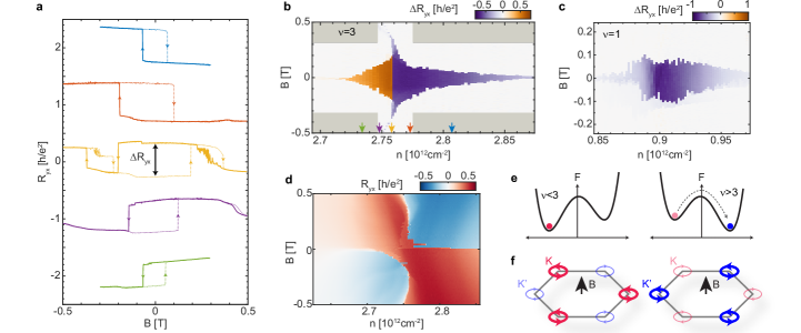
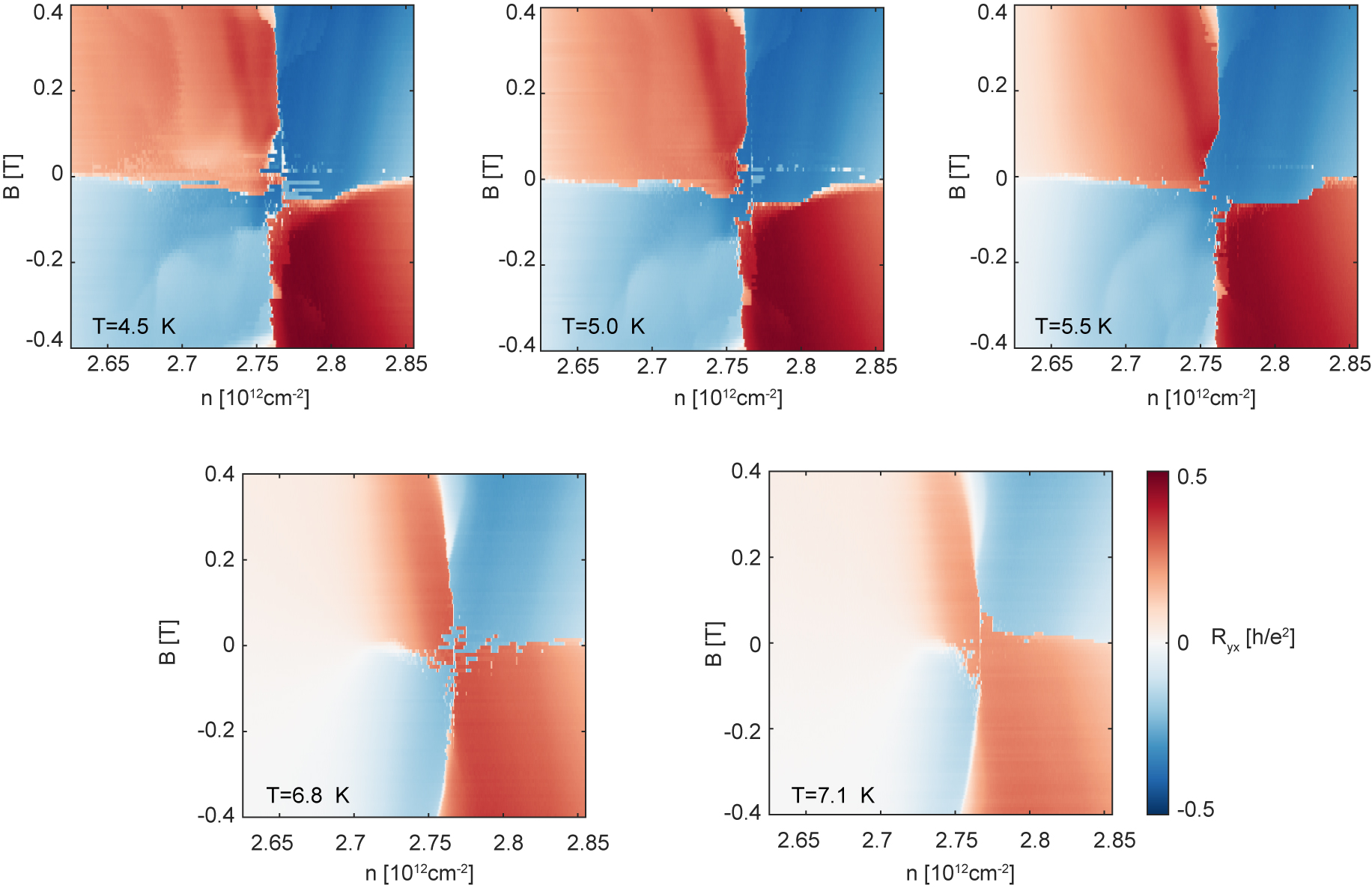
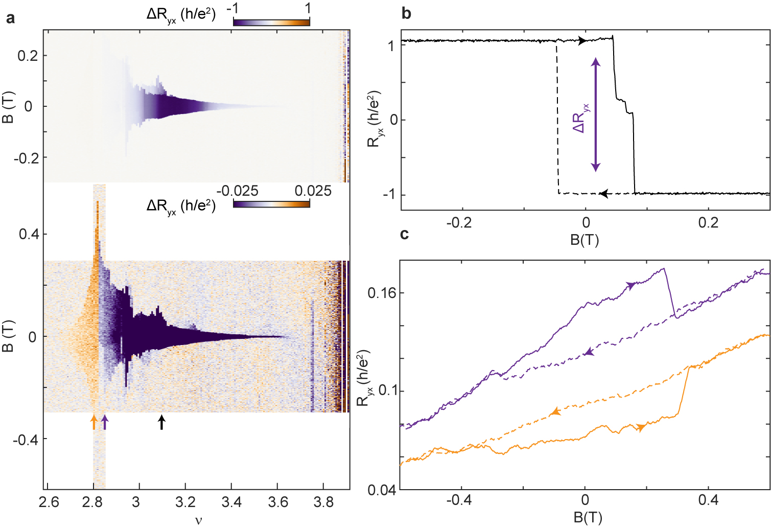
Striking new phenomena are, however, observed in the -dependence of the Hall effect. Specifically, whereas changes smoothly as a function of near the orbital Chern insulator, it exhibits erratic switching behavior near (Figure 2d,e). To investigate this phenomenon, we perform a dense series of hysteresis loop measurements in the vicinity of at higher temperature, where we expect that domain wall pinning is weaker and hysteretic effects are somewhat suppressed. While the sign of the anomalous Hall resistance is constant near , it reverses abruptly upon crossing (see Figs. 3a-c). The sign reversal occurs with minimal change in the magnitude of , which remains close to the quantized value. This suggests that the reversal occurs via a change in the product of the magnetization sign and the Chern number sign, which we refer to as the magnetic state. This is further evidenced by the - map of (see Figs. 3d), which shows that the changes sign at , corresponding to . An additional manifestation of the inversion of the sign of the magnetization of a given magnetic state is the abrupt upturn in the coercive field in the close vicinity of the reversal point shown in Figure 3b. This phenomenon is qualitatively consistent with a picture in which the total magnetization changes sign for a fixed sense of valley polarization by passing through zero; near , the coupling to the magnetic field vanishes leading to a divergence of the coercive field.
We propose that the magnetization reversal arises from the unique features of orbital Chern insulators. In particular, the protected edge states required by their nontrivial topology are occupied and contribute to the magnetization when the insulator is slightly -doped, but not when it is slightly -dopedZhu et al. (2020). The edge state contribution leads to a jump in the magnetization across the Chern insulator gap,
| (1) |
where is the electron mass, is the unit cell area, is the gap, and is the Bohr magneton. While this effect is present in all Chern insulators, it is negligible in magnetically doped topological insulatorsChang et al. (2013) where time-reversal symmetry is broken primarily by spontaneous spin-polarization. In these systems, the total spin magnetization is of order . Since is on the order of a few meV, and the edge-state orbital magnetization is dwarfed by spin magnetization. In graphene moiré orbital Chern insulators the bulk orbital magnetization is again of order Zhu et al. (2020); Tschirhart et al. (2020). However, the large unit cell area allows for the prefactor in Eq. 1 to be of comparable or larger magnitude. When this edge state contribution is sufficiently large, it can lead to a reversal in the sign of the net magnetization across the energy gap. For instance, taking measured energy gaps for quantum anomalous Hall states in twisted bilayer grapheneSerlin et al. (2020) produces an estimate of . Indeed, a reexamination of transport data from the tBLG device aligned to hexagonal boron nitride studied in Ref. Serlin et al., 2020 finds a similar, though much less dramatic, change in the sense of the hysteresis loop accompanied by a similar divergence of the coercive field near (though not precisely at) (see Figure E8). We note that the magnetization of an orbital magnet can in principle change sign at any filling factor, but that it is more likely at integer because the magnetization is discontinuous at this density.The conditions under which the reversal occur are discussed in Methods.
Electrical switching of magnetic states
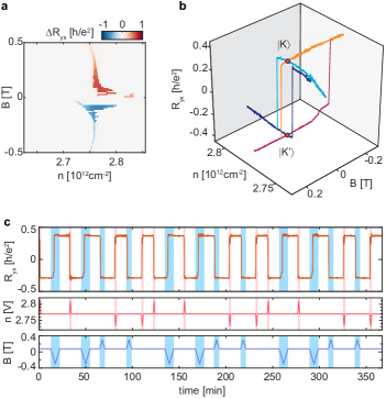
Because an external magnetic field favors the state with magnetization aligned with the field, changing the sign of is predicted to drive a reversal of the valley polarization as the chemical potential crosses the gap (see Figure 3e-f). The quantized Hall effect sign reversal is thus due to a change in magnetic state, in contrast to previously observed anomalous Hall effect sign reversalsChiba et al. (2010); Zhang et al. (2020) arising from a change in the sign of the total anomalous Hall effect for a given magnetic state. As a result, electric field induced hysteretic behavior is possible in our case since the two states are separated by an energy barrier. Fig. 4a depicts the difference (again denoted ) between traces and retraces of field-effect tuned density, acquired as is stepped. Near , shows a finite signal in this channel, indicating hysteresis in gate voltage sweeps at fixed magnetic fields as high as several hundred millitesla.
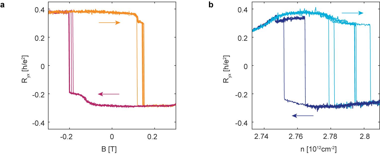
Electric field control of magnetic states provides a reliable experimental knob to realize nonvolatile switching of magnetization. We find that at 80 mT, = cm-2, and K, states of opposite polarization can be controllably switched using either excursions in or , as shown in Figure 4b. Figure 4c shows this principle applied to nonvolatile switching of the magnetic state using both excursions at constant and excursions at constant . Switches occur with perfect fidelity and appear to be indefinitely nonvolatile at this temperature. We note that as for current- and magnetic field-driven switching, the excellent reproducibility of field-effect switching ultimately arises from the absence of states with partial or intermediate valley polarization, or equivalently the extreme anisotropy inherent in a purely orbital two dimensional magnet.
Orbital magnets realized at room temperature would be immediately applicable as embedded magnetic memory in logic devices. Candidates for higher temperature operation include other moiré systems in which the lattice constant is smaller and the correlation energy consequently larger, assembled either by van der Waals stacking or using non-epitaxial growth techniquesBeekman et al. (2014). Even restricted to cryogenic temperatures, there exist several immediate opportunities that leverage gate switchable chirality in a quantum anomalous Hall system. As a simple example, orbital Chern insulators could be used as the central elements in reconfigurable and compact microwave circulatorsViola and DiVincenzo (2014), which may be useful for scaling up quantum information processing. Meanwhile, integrating orbital Chern insulators with superconductors may permit new device architectures devoted to the detection and manipulation of extended Majorana zero modesLian et al. (2018). Our results highlight the novel opportunities for controlling functionality that arise from the realization of purely orbital magnetic systems.
Methods
Device fabrication
Van-der-Waals heterostructures for tMBG devices are fabricated by a dry transfer technique based on a polycarbonate film on top of a polydimethyl siloxane (PDMS) stamp. The heterostructure is assembled in two steps to minimize the chance to disturb the twist angle at the critical monolayer-bilayer interface. First a two layer stack with hBN at the top and graphite layer at the bottom is picked up and transferred to a bare wafer. This partial stack is annealed in vacuum at C to remove polymer residues from the top surface. A second stack consisting (from top to bottom) of hBN-FLG-hBN-MLG-BLG(where FLG, MLG and BLG are few-layer, monolayer and bilayer graphene, respectively) is then assembled and transferred on top of the first one. Crucially, the angle registry between the MLG and BLG is ensured by starting from a single exfoliated flake that includes both MLG and BLG domains. The flake is then cut with a conducting atomic force microscope tip in air (see Extended Data Fig. E1). The MLG piece is picked up using a PDMS stamp and an interlayer twist introduced by substrate rotation, and then the BLG pieced picked up. All flakes except MLG and BLG are picked up at approximately C; the MLG, BLG, and the transfer to the final substrate are made at C to preserve the twist angle of the structure. Devices are then fabricated using standard e-beam lithography and etching, and edge contacts are made by deposition of Cr/Pd/Au (1.5/15/250 nm).
Device characterization
Transport measurements were performed using SRS lock-in amplifier, scurrent preamplifiers (DL Instruments) and voltage preamplifiers (SRS) with typical excitations in the range 1-10 nA at 17.77 Hz. Measurements were performed in either a cryogen free dilution refrigerator, with the sample in vacuum, or in the case of Extended Data Fig. E3, in a wet variable temperature insert with the sample in helium vapor.
For devices D1 and D2, the twist angle was determined from the position of the correlated insulating states. For devices D3 and D4 the twist angle was determined from the periodicity of the Hofstadter features observed in magnetic field that arise from the interplay of the moiré superlattice period and magnetic length.
Band structure simulations
Band structure simulations are performed within a continuum model analogous to that of ReferenceBistritzer and MacDonald (2011) for the coupling between the top and middle layers while the middle and bottom layers are treated as Bernal-stacked bilayer graphene. More details are in the Supplementary Information (SI).
Electrical reversibility
Why is the field-effect reversibility so robust in tMBG at , but weak in twisted bilayer graphene at and absent at other filling factors in either system? Field reversibility requires that the edge state contribution to the magnetization, , reverses the sign of the total magnetization. Our calculations for both tMBG and twisted bilayer graphene aligned to hBN indicate that and –defined as the total magnetization when the chemical potential is at the bottom of the gap—normally have opposite sign. To ensure field reversibility, one thus wants to maximize the magnitude of the edge state contribution while minimizing the magnitude of the bulk contribution. The large Chern numbers in tMBG are certainly helpful in this regard, as they increase . In addition, our theoretical analysis indicates that in odd layer systems, exchange splitting between bands arising from valley polarization further decreases the magnitude of . This effect, which includes contributions from bands far from the Fermi level, is present in tMBG but absent in twisted bilayer (see SI for details). The exchange contribution is expected to be larger at than at , possibly explaining why we see reversible Chern insulators at but conventional Chern insulators at in tMBG.
References
- Matsukura et al. (2015) F. Matsukura, Y. Tokura, and H. Ohno, Nature Nanotechnology 10, 209 (2015).
- Jiang et al. (2018) S. Jiang, J. Shan, and K. F. Mak, Nature Materials (2018), 10.1038/s41563-018-0040-6.
- Sharpe et al. (2019) A. L. Sharpe, E. J. Fox, A. W. Barnard, J. Finney, K. Watanabe, T. Taniguchi, M. A. Kastner, and D. Goldhaber-Gordon, Science 365, 605 (2019).
- Serlin et al. (2020) M. Serlin, C. L. Tschirhart, H. Polshyn, Y. Zhang, J. Zhu, K. Watanabe, T. Taniguchi, L. Balents, and A. F. Young, Science 367, 900 (2020).
- Chen et al. (2020) G. Chen, A. L. Sharpe, E. J. Fox, Y.-H. Zhang, S. Wang, L. Jiang, B. Lyu, H. Li, K. Watanabe, T. Taniguchi, Z. Shi, T. Senthil, D. Goldhaber-Gordon, Y. Zhang, and F. Wang, Nature 579, 56 (2020).
- Lu et al. (2019) X. Lu, P. Stepanov, W. Yang, M. Xie, M. A. Aamir, I. Das, C. Urgell, K. Watanabe, T. Taniguchi, G. Zhang, A. Bachtold, A. H. MacDonald, and D. K. Efetov, Nature 574, 653 (2019).
- Xie and MacDonald (2020) M. Xie and A. MacDonald, Physical Review Letters 124, 097601 (2020).
- Bultinck et al. (2020) N. Bultinck, S. Chatterjee, and M. P. Zaletel, Phys. Rev. Lett. 124, 166601 (2020).
- Zhang et al. (2019a) Y.-H. Zhang, D. Mao, and T. Senthil, Phys. Rev. Research 1, 033126 (2019a).
- Liu and Dai (2020) J. Liu and X. Dai, arXiv:1911.03760 [cond-mat] (2020).
- Wu and Das Sarma (2020) F. Wu and S. Das Sarma, Phys. Rev. Lett. 124, 046403 (2020).
- Chatterjee et al. (2020) S. Chatterjee, N. Bultinck, and M. P. Zaletel, Phys. Rev. B 101, 165141 (2020).
- Repellin et al. (2020) C. Repellin, Z. Dong, Y.-H. Zhang, and T. Senthil, Phys. Rev. Lett. 124, 187601 (2020).
- Alavirad and Sau (2019) Y. Alavirad and J. D. Sau, arXiv:1907.13633 [cond-mat] (2019).
- Ma et al. (2019) Z. Ma, S. Li, Y.-W. Zheng, M.-M. Xiao, H. Jiang, J.-H. Gao, and X. C. Xie, arXiv:1905.00622 [cond-mat] (2019).
- Park et al. (2020) Y. Park, B. L. Chittari, and J. Jung, Phys. Rev. B 102, 035411 (2020).
- Rademaker et al. (2020) L. Rademaker, I. V. Protopopov, and D. A. Abanin, Phys. Rev. Research 2, 033150 (2020).
- Chang et al. (2013) C.-Z. Chang, J. Zhang, X. Feng, J. Shen, Z. Zhang, M. Guo, K. Li, Y. Ou, P. Wei, L.-L. Wang, Z.-Q. Ji, Y. Feng, S. Ji, X. Chen, J. Jia, X. Dai, Z. Fang, S.-C. Zhang, K. He, Y. Wang, L. Lu, X.-C. Ma, and Q.-K. Xue, Science 340, 167 (2013).
- Zhu et al. (2020) J. Zhu, J.-J. Su, and A. H. MacDonald, arXiv:2001.05084 [cond-mat] (2020).
- Haldane (1988) F. D. M. Haldane, Phys. Rev. Lett. 61, 2015 (1988).
- Song et al. (2015) J. C. W. Song, P. Samutpraphoot, and L. S. Levitov, Proceedings of the National Academy of Sciences 112, 10879 (2015).
- Zhang et al. (2019b) Y.-H. Zhang, D. Mao, Y. Cao, P. Jarillo-Herrero, and T. Senthil, Physical Review B 99, 075127 (2019b).
- Liu et al. (2019a) J. Liu, Z. Ma, J. Gao, and X. Dai, Physical Review X 9, 031021 (2019a).
- Bistritzer and MacDonald (2011) R. Bistritzer and A. H. MacDonald, Proceedings of the National Academy of Sciences 108, 12233 (2011).
- Cao et al. (2018) Y. Cao, V. Fatemi, A. Demir, S. Fang, S. L. Tomarken, J. Y. Luo, J. D. Sanchez-Yamagishi, K. Watanabe, T. Taniguchi, E. Kaxiras, R. C. Ashoori, and P. Jarillo-Herrero, Nature 556, 80 (2018).
- Chen et al. (2019) G. Chen, L. Jiang, S. Wu, B. Lyu, H. Li, B. L. Chittari, K. Watanabe, T. Taniguchi, Z. Shi, J. Jung, Y. Zhang, and F. Wang, Nature Physics 15, 237 (2019).
- Shen et al. (2020) C. Shen, Y. Chu, Q. Wu, N. Li, S. Wang, Y. Zhao, J. Tang, J. Liu, J. Tian, K. Watanabe, T. Taniguchi, R. Yang, Z. Y. Meng, D. Shi, O. V. Yazyev, and G. Zhang, Nature Physics , 1 (2020).
- Liu et al. (2019b) X. Liu, Z. Hao, E. Khalaf, J. Y. Lee, K. Watanabe, T. Taniguchi, A. Vishwanath, and P. Kim, arxiv (2019b).
- Cao et al. (2020) Y. Cao, D. Rodan-Legrain, O. Rubies-Bigorda, J. M. Park, K. Watanabe, T. Taniguchi, and P. Jarillo-Herrero, Nature , 1 (2020).
- Burg et al. (2019) G. W. Burg, J. Zhu, T. Taniguchi, K. Watanabe, A. H. MacDonald, and E. Tutuc, Physical Review Letters 123, 197702 (2019).
- He et al. (2020) M. He, Y. Li, J. Cai, Y. Liu, K. Watanabe, T. Taniguchi, X. Xu, and M. Yankowitz, Nature Physics , 1 (2020).
- Streda (1982) P. Streda, J. Phys. C: Solid State Phys. 15 (1982).
- Tschirhart et al. (2020) C. L. Tschirhart, M. Serlin, H. Polshyn, A. Shragai, Z. Xia, J. Zhu, Y. Zhang, K. Watanabe, T. Taniguchi, M. E. Huber, and A. F. Young, arXiv:2006.08053 [cond-mat] (2020).
- Chiba et al. (2010) D. Chiba, A. Werpachowska, M. Endo, Y. Nishitani, F. Matsukura, T. Dietl, and H. Ohno, Physical Review Letters 104, 106601 (2010).
- Zhang et al. (2020) S. Zhang, R. Wang, X. Wang, B. Wei, B. Chen, H. Wang, G. Shi, F. Wang, B. Jia, Y. Ouyang, F. Xie, F. Fei, M. Zhang, X. Wang, D. Wu, X. Wan, F. Song, H. Zhang, and B. Wang, Nano Letters 20, 709 (2020).
- Beekman et al. (2014) M. Beekman, C. L. Heideman, and D. C. Johnson, Semiconductor Science and Technology 29, 064012 (2014).
- Viola and DiVincenzo (2014) G. Viola and D. P. DiVincenzo, Physical Review X 4, 021019 (2014).
- Lian et al. (2018) B. Lian, X.-Q. Sun, A. Vaezi, X.-L. Qi, and S.-C. Zhang, Proceedings of the National Academy of Sciences 115, 10938 (2018).
- Yoo et al. (2019) H. Yoo, R. Engelke, S. Carr, S. Fang, K. Zhang, P. Cazeaux, S. H. Sung, R. Hovden, A. W. Tsen, T. Taniguchi, K. Watanabe, G.-C. Yi, M. Kim, M. Luskin, E. B. Tadmor, E. Kaxiras, and P. Kim, Nature Materials 18, 448 (2019).
- Neto et al. (2009) A. H. C. Neto, F. Guinea, N. M. R. Peres, K. S. Novoselov, and A. K. Geim, Reviews of Modern Physics 81 (2009).
- Jung and MacDonald (2014) J. Jung and A. H. MacDonald, Physical Review B 89, 035405 (2014).
- McCann and Koshino (2013) E. McCann and M. Koshino, Reports on Progress in Physics 76, 056503 (2013).
- Raoux et al. (2015) A. Raoux, F. Piéchon, J.-N. Fuchs, and G. Montambaux, Physical Review B 91, 085120 (2015).
acknowledgments
The authors acknowledge discussions with J. Checkelsky, S. Chen, C. Dean, M. Yankowitz, D. Reilly, I. Sodemann, and M. Zaletel for discussions. Work at UCSB was primarily supported by the ARO under MURI W911NF-16-1-0361. Measurements of twisted bilayer graphene (Extended Data Fig. E8) and measurements at elevated temperatures (Extended Data Fig. E3) were supported by a SEED grant and made use of shared facilities of the UCSB MRSEC (NSF DMR 1720256), a member of the Materials Research Facilities Network (www.mrfn.org). AFY acknowledges the support of the David and Lucille Packard Foundation under award 2016-65145. AHM and JZ were supported by the National Science Foundation through the Center for Dynamics and Control of Materials, an NSF MRSEC under Cooperative Agreement No. DMR-1720595, and by the Welch Foundation under grant TBF1473. CLT acknowledges support from the Hertz Foundation and from the National Science Foundation Graduate Research Fellowship Program under grant 1650114. KW and TT acknowledge support from the Elemental Strategy Initiative conducted by the MEXT, Japan, Grant Number JPMXP0112101001, JSPS KAKENHI Grant Numbers JP20H00354 and the CREST(JPMJCR15F3), JST.
Author contributions
HP, MAK, and YZ fabricated the devices. HP, FY, CLT and MS performed the measurements, advised by AFY. JZ and AHM performed the band structure calculations. KW and TT grew the hexagonal boron nitride crystals. HP, AHM, and AFY wrote the manuscript with input from all other authors.
Competing interests
The authors declare no competing interests.
Data availability
Source data are available for this paper. All other data that support the plots within this paper and other findings of this study are available from the corresponding author upon reasonable request.
Supplementary Information
I Moiré miniband simulation
The valley- and spin-projected -space continuum model Hamiltonian of tMBG acts on six-component spinors that describe slow spatial variations of the carbon -orbital amplitudes on each of the trilayer’s six sublattices. Using a momentum-space representation for the spinor components, the Hamiltonian is
| (S1) |
Here is the interlayer tunneling between the monolayer and the adjacent Bernal layerBistritzer and MacDonald (2011),
| (S2) |
where the sublattice-dependent hopping matrices and the momentum jumps are defined in Ref. Bistritzer and MacDonald, 2011. In our calculations we took the tunneling strength to be meV and reduced the diagonal elements of to meV to accountYoo et al. (2019) for corrugation and strain effects. For the intralayer Hamiltonains we used -band Dirac modelsNeto et al. (2009) that allow for sublattice-dependent energies and :
| (S3) |
where
| (S4) |
are three honeycomb lattice nearest neighbour vectors, and is the crystal momentum measured from graphene Brillouin-zone corner. We adopt the intralayer nearest neighbour hopping amplitude meV ab initio calculated in Bernal-stacked bilayer grapheneJung and MacDonald (2014). The corresponding Dirac velocity m/s is smaller than the commonly used value m/s in twisted bilayer graphene. It should be noted that Dirac velocity in the effective continuum model in Eq.(S1) would modify the band structure, larger increases the single-particle band gap at charge neutrality. Finally, is the interlayer tunneling between the middle and bottom Bernal-stacked layers:
| (S5) |
Here we define the interlayer hopping parameters as
| (S6) |
are -orbitals. Note that some of these definitions are different in signs with the widespreadly used Slonczewski-Weiss-McClure model parametersMcCann and Koshino (2013). We take meV, meV and meVJung and MacDonald (2014) in our calculations. The sublattice energies were taken to be identical on both sublattices within each graphene layer, thereby ignoring the possible influence of the hBN encapsulating, but layer-dependent on-site energies are considered to account for displacement fields. The potential energy difference between layers was taken to be with the displacement field, Å the graphene interlayer separation, and a background dielectric constant that accounts for remote-band polarizations in graphene sheets.
II Self-consistent Hartree approximation
Self-consistent Hartree approximation is extensively used to capture the band structure at finite carrier densities. We ignore the exchange interaction between carriers even though it was shownXie and MacDonald (2020) to be important in magic angle twisted bilayer graphene.
In a dual-gated system, the external electric field and carrier density can be tuned individually. Assume a positive external displacement field is in the direction as depicted in Fig.1b (monolayer to bilayer) in the main text, onsite energies on top (monolayer), middle and bottom layers are respectively , and . For a fixed total electron density , after charge redistribution the induced potential energies are
| (S7) |
where , and are electron densities on each layer and are calculated by summing over wavefunction squares
| (S8) |
moiré Brillouin zone, , and are band, layer and sublattice indices. Chemical potential is determined by total electron density. is the background density from negative Fermi seas. The integer 4 takes into account four flavors (two valleys and two spins) as we use a valley- and spin-polarized continuum Hamiltonian in Eq. (S1).
III Electrical Reversibility
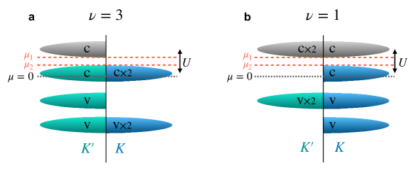
Orbital Chern insulators have been observed in both tMBG with a finite displacement field and in magic-angle twisted bilayer graphene (tBLG) encapsulated by hexagonal boron nitride (hBN). We note that the magnetization of an orbital Chern insulator can in principle change sign for a given sense of valley polarization at any band filling factor , but that it is overwhelmingly more likely to change sign at integer where the magnetization can be discontinuous. We therefore focus on the issue of when the magnetization is likely to change sign across a gap characterized by a non-zero Chern number. The magnetization of tBLG orbital Chern insulators has been previously discussed using a continuum model approachZhu et al. (2020). Here we use the same approach to compare theoretical expectations for magnetizations on opposite sides of the and gaps for both tBLG and tMBG.
As explained inZhu et al. (2020) the continuum model magnetization is a sum over separate contributions from different spin and valley flavors. We will account for time-reversal-symmetry breaking using a simplified mean-field approach in which the quasiparticle energies for a particular flavor are shifted downward by a momentum-independent exchange when the lowest energy conduction band is occupied for that flavor, leaving the quasiparticle wavefunctions unchanged. This prescription approximates the predictions of self-consistent Hartree-Fock mean-field theoryXie and MacDonald (2020). The resulting mean-field bands are illustrated schematically in Fig. S1. Insulating states occur when the energy shift is greater than the bandwidth of the conduction band, resulting in a gap
| (S9) |
Here is the gap between the valence and conduction bands in the absence of the exchange interaction shift . If we choose the zero of energy at the middle of , it follows that for both and , the bottom of the conduction band of the unoccupied flavor (or flavors) is at energy . The energy at the top of the highest occupied band is .
The requirement for a magnetization sign change across the gap can be expressed in terms of the magnetizations at chemical potential () and at chemical potential ():
| (S10) |
and differ by the magnetization jump across the gap, , which is proportional to the Chern number of the time-reversal partner of the unoccupied bands. Assuming higher occupation of valley , the case shown in Fig. S1,
| (S11) |
where is the Chern number of the flat conduction band in valley . Magnetization sign reversal will occur if is large enough and has the correct sign:
| (S12) |
Here is the total magnetization when the edge states in the gap are unoccupied, i.e. when the chemical potential is at the bottom of the gap: .
In order to identify the influence of the flavor-dependent energy shifts and occupations in the broken time-reversal symmetry state, we write the magnetization in the following form ():
| (S13) |
Here is a band index, is a spin/valley flavor index, is the set of flavors that have had energies shifted by conduction band occupation, is the band occupation, is the band Chern number, and is the portion of the magnetization defined in Ref. Zhu et al. (2020), evaluated with the zero of energy located at the middle of the gap for that flavor. In Eq. (S13) we have used that the magnetization contribution of an occupied band shifts by when band energies are rigidly shifted by .
When we apply Eq. (S13) to we have two occupied conduction bands in valley and one occupied conduction band in valley , as shown in Fig. S1a. Since the band occupation numbers of all valence bands are equal and it follows that
| (S14) |
where is the part magnetization of the lowest energy conduction band in valley . Since opposite valleys also have opposite Chern numbers, the sum of the Chern numbers over all occupied bands comes only from the uncompensated conduction bands and is . On the other hand the sum of the Chern numbers over all occupied bands that suffer an energy shift is where is the Chern number of the highest energy valence band in valley and is the corresponding sum over all remote valence bands. The final expression for the magnetization as a function of chemical potential in the gap is
| (S15) |
The same equation applies for since the two conditions differ by changing the occupation numbers and shifting the energies of two bands that are in opposite valleys. We emphasize that the energy shift contribution is proportional to the sum of the Chern numbers of all shifted bands, and has a contribution from the valence bands because the energy shifts are valley-dependent. On the other hand, the chemical potential shift contribution is proportional to the sum of all occupied-band Chern numbers, and this does not have a valence band contribution.

In Fig. S2a, we plot Chern numbers , and of tMBG vs. displacement field . and are both independent of . The Chern numbers are obtained by momentum space integration. The two flat bands touch either at or near the yellow-shaded regions (where the numerical results become inaccurate), transferring Berry curvature between them. The half-odd-integer value of is expected in a continuum model with an odd number of graphene layers since the Berry curvature integrated over all valence band states is in the decoupled trilayer limit when sublattice symmetry is weakly broken. When moiré bands are formed, the integrated Berry curvature of each isolated moiré miniband must however be an integer. In gate biased tMBG our results show that integers are achieved by transferring Berry curvature between conduction and valence bands with a sense that depends on the sign of . Note that both and , but not their difference, is dependent on . This feature of our magnetization calculations is the continuum model manifestation of the band-Hamiltonian propertyRaoux et al. (2015) that the orbital magnetization vs. curve over some narrow interval can be shifted by a constant by band rearrangements at very remote energies. Our continuum model estimates are therefore more uncertain for the mean value of and than they are for their difference .

As a comparison, we also show the corresponding Chern numbers (Fig. S2b-d) of tBLG. The driver of non-trivial topology in the valley-projected bands in this case is sublattice symmetry breaking by encapsulating hBN layers (or spontaneously due to electron electron interactions) which induces masses (non-zero values of ) in adjacent layers . For one-side alignment case, i.e. only one graphene layer is nearly aligned with hBN, the mass on one graphene layer and the mass on the other graphene layer . In this case, shown in Fig. S2b, Chern numbers of flat bands are and the total Chern number of all remote valence bands is . Moiré miniband formation no longer forces a transfer of Berry curvatures between conduction and valence bands, and none occurs. For two-side alignment case, when , corresponding to both graphene layers being nearly aligned with the surrounding hBN layers and having the same relative orientation, the flat band Chern numbers shown in Fig. S2c are again , and the total Chern number of all remote valence bands is again . If both graphene layers are nearly aligned but have opposite relative orientations with hBN, i.e. , the Chern numbers vanish as shown in Fig. S2d.
Given these results for the Chern numbers the following two equations apply at both and at in tMBG:
| (S16) |
and
| (S17) |
The corresponding equations for tBLG are:
| (S18) |
and
| (S19) |
In the tMBG case, polarization toward valley implies a positive conduction band Chern number for positive displacement field, and therefore implies that . Electrical reversal is possible only if is negative for positive displacement field and the gap is larger than . For the tBLG case, polarization toward valley implies a positive (negative) conduction band Chern number for negative (positive) . Electrical reversal therefore requires that is negative (positive) for negative (positive) and that the gap is larger than .
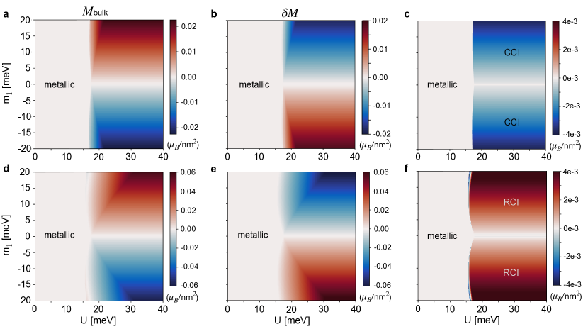
Figures S3a-c show the dependence of , , and in tMBG on and after self-consistent Hartree approximation. It should be noted that these results are calculated using a phenomenologically increased band gap , on the order of 10 meV, to match experimental band gap measurements, owing to the fact that Hartree approximation alone will underestimate the gap. As we mentioned above, is not accurately captured in our continuum model even though it is essential in the sign-reversal effect. Gapless regions that correspond to () or overlapping conduction and valence bands are marked as ”metallic” in Fig. S3. Figure S3c identifies regions where and are opposite in sign and has a larger magnitude (i.e. Eq. (S12) is satisfied) as reversible Chern insulators (RCI), and other regions where the state is insulating as conventional Chern insulators (CCI). We see that RCI states occur for positive displacement fields when the exchange energy is large enough. Since we expect the effective value of to be smaller when the filling factor is closer to zero and the overall flat band system is therefore closer to half-filling – enhancing screening and correlation corrections to mean field theory, the experimental finding that RCI state occurs for but not for is consistent with Fig. S3. It should be pointed out that we are not considering hBN alignments, which break sublattice symmetry in tMBG, in our numerical calculations. However some specific hBN alignments can make the magnetization sign-reversal effect more robust numerically.
As a comparison, we also show the corresponding phase diagrams (Fig. S4) of tBLG. Note that insulating states appear only beyond a minimum but require only infinitesimal masses. Interestingly we find CCI states for one-side hBN alignment and RCI states for two-side hBN alignment. As we see in Fig. S4 the difference can be traced to a difference in the signs of in the two cases:
| (S20) |
The sign of is dependent on a competition between the and the Chern number term in Eq. (S18). Two-sided alignment increases sublattice-symmetry breaking and increases both the magnitudes of the conduction-valence energy-gap and . In our numerical calculations, however, the magnitudes of is doubled by two-side alignment, whereas the energy gap is increased by more than a factor of three, changing the sign of . Since we expect that electron-electron interactions will also enhance the energy gap by a larger factor than they enhance , RCI behavior likely occurs for one-side alignment as well when interaction effects are described in greater detail.
