Electrically tunable correlated and topological states in twisted monolayer-bilayer graphene
Twisted van der Waals heterostructures with flat electronic bands have recently emerged as a platform for realizing correlated and topological states with an extraordinary degree of control and tunability Cao2018a ; Cao2018b ; Yankowitz2019 ; Lu2019 ; Stepanov2019 ; Saito2019 ; Sharpe2019 ; Serlin2020 ; Arora2020 ; Shen2020 ; Liu2019 ; Cao2019 ; Burg2019 ; He2020 ; Chen2019 ; Chen2019sctrilayer ; Chen2020 ; Tang2020 ; Regan2020 ; Wang2019 . In graphene-based moiré heterostructures, the correlated phase diagram and band topology depend strongly on the number of graphene layers Cao2018a ; Cao2018b ; Yankowitz2019 ; Sharpe2019 ; Lu2019 ; Serlin2020 ; Stepanov2019 ; Saito2019 ; Arora2020 ; Shen2020 ; Liu2019 ; Cao2019 ; Burg2019 ; He2020 ; Chen2019 ; Chen2019sctrilayer ; Chen2020 , their relative stacking arrangement Chen2019 ; Chen2019sctrilayer ; Chen2020 , and details of the external environment from the encapsulating crystals Chen2019 ; Chen2019sctrilayer ; Chen2020 ; Sharpe2019 ; Serlin2020 ; Arora2020 . Here, we report that the system of twisted monolayer-bilayer graphene (tMBG) hosts a variety of correlated metallic and insulating states, as well as topological magnetic states. Because of its low symmetry, the phase diagram of tMBG approximates that of twisted bilayer graphene when an applied perpendicular electric field points from the bilayer towards the monolayer graphene, or twisted double bilayer graphene when the field is reversed. In the former case, we observe correlated states which undergo an orbitally driven insulating transition above a critical perpendicular magnetic field. In the latter case, we observe the emergence of electrically tunable ferromagnetism at one-quarter filling of the conduction band, with a large associated anomalous Hall effect. Uniquely, the magnetization direction can be switched purely with electrostatic doping at zero magnetic field. Our results establish tMBG as a highly tunable platform for investigating a wide array of tunable correlated and topological states.
In select van der Waals (vdW) heterostructures, coupling to a moiré superlattice renormalizes the band structure and results in nearly flat electronic bands. These systems act as highly-tunable platforms capable of hosting a variety of correlated and topological ground states, including correlated insulating (CI) states, superconductivity, and ferromagnetism with an associated quantum anomalous Hall effect (QAHE) Cao2018a ; Cao2018b ; Yankowitz2019 ; Lu2019 ; Stepanov2019 ; Saito2019 ; Sharpe2019 ; Serlin2020 ; Arora2020 ; Shen2020 ; Liu2019 ; Cao2019 ; Burg2019 ; He2020 ; Chen2019 ; Chen2019sctrilayer ; Chen2020 ; Tang2020 ; Regan2020 ; Wang2019 . In moiré heterostructures composed entirely of graphene, the correlated phase diagram depends sensitively on the number of graphene sheets. In twisted bilayer graphene (tBLG) — two rotated sheets of monolayer graphene — CI states and superconductivity can be induced and tuned by changing the twist angle Cao2018a ; Cao2018b ; Yankowitz2019 ; Lu2019 ; Stepanov2019 ; Saito2019 and by applying pressure Yankowitz2019 . In addition, ferromagnetism and a QAHE can be obtained in the system by further rotationally aligning tBLG with a boron nitride (BN) substrate Sharpe2019 ; Serlin2020 . In twisted double bilayer graphene (tDBG) — two rotated sheets of Bernal-stacked bilayer graphene — spin-polarized CI states are observed that can be further tuned by application of a perpendicular electric field Shen2020 ; Liu2019 ; Cao2019 ; Burg2019 ; He2020 . Finally, three layers of rhombohedrally-stacked graphene rotationally aligned with BN can also manifest CI states and ferromagnetism with non-trivial band topology Chen2019 ; Chen2019sctrilayer ; Chen2020 .
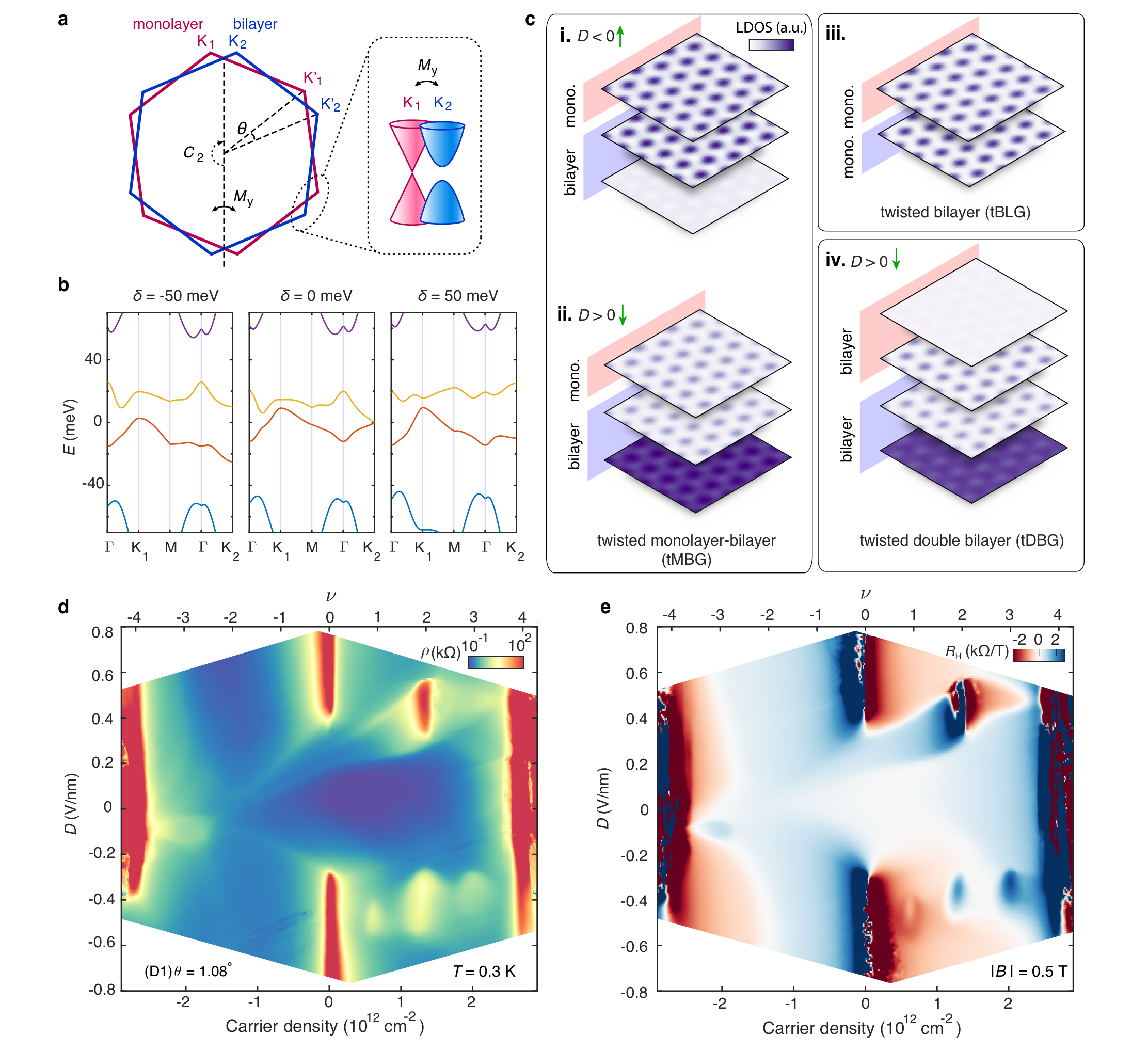
Heterostructures comprising rotated sheets of monolayer and Bernal-stacked bilayer graphene have so far not been investigated experimentally, but are theoretically promising candidates to host correlated and topological states owing to their flat electronic bands with non-zero Chern numbers SuarezMorell2013 ; Ma2019 ; Liu2019theory . Twisted monolayer-bilayer graphene (tMBG) has low crystal symmetry, breaking both two-fold rotation, , and mirror reflection, . The former exchanges opposite valleys within the same layer, and the latter exchanges the top and bottom components of the twisted heterostructure (Fig. 1a). Consequentially, these states are anticipated to be uniquely tunable with a simple combination of a single twist angle, , gate doping, , and perpendicular displacement field, , without any additional complicating conditions involving an internal crystal stacking configuration Chen2019 ; Chen2019sctrilayer ; Chen2020 or coupling to a secondary moiré pattern Sharpe2019 ; Serlin2020 .
Here, we investigate electrical transport in dual-gated tMBG devices over a small range of twist angles, . We find that the correlated phase diagram of tMBG can approximately resemble either tBLG or tDBG depending on the direction of . When points from the bilayer towards the monolayer graphene, we observe correlated states at all integer filling factors similar to tBLG, with the exception that superconductivity does not occur. Although correlations appear to be weaker than in tBLG, CI states emerge above a critical perpendicular magnetic field. When the direction of the electric field is flipped, we observe a spin-polarized CI state at half filling of the conduction band similar to tDBG. Remarkably, tMBG additionally manifests correlated magnetic states with intrinsic topological order in this configuration, which can be controlled by , , and . Our work thus provides a means of realizing a wide array of tunable correlated and topological states within a single material platform.
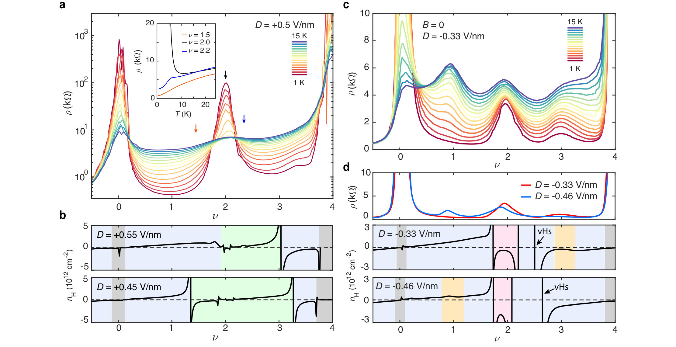
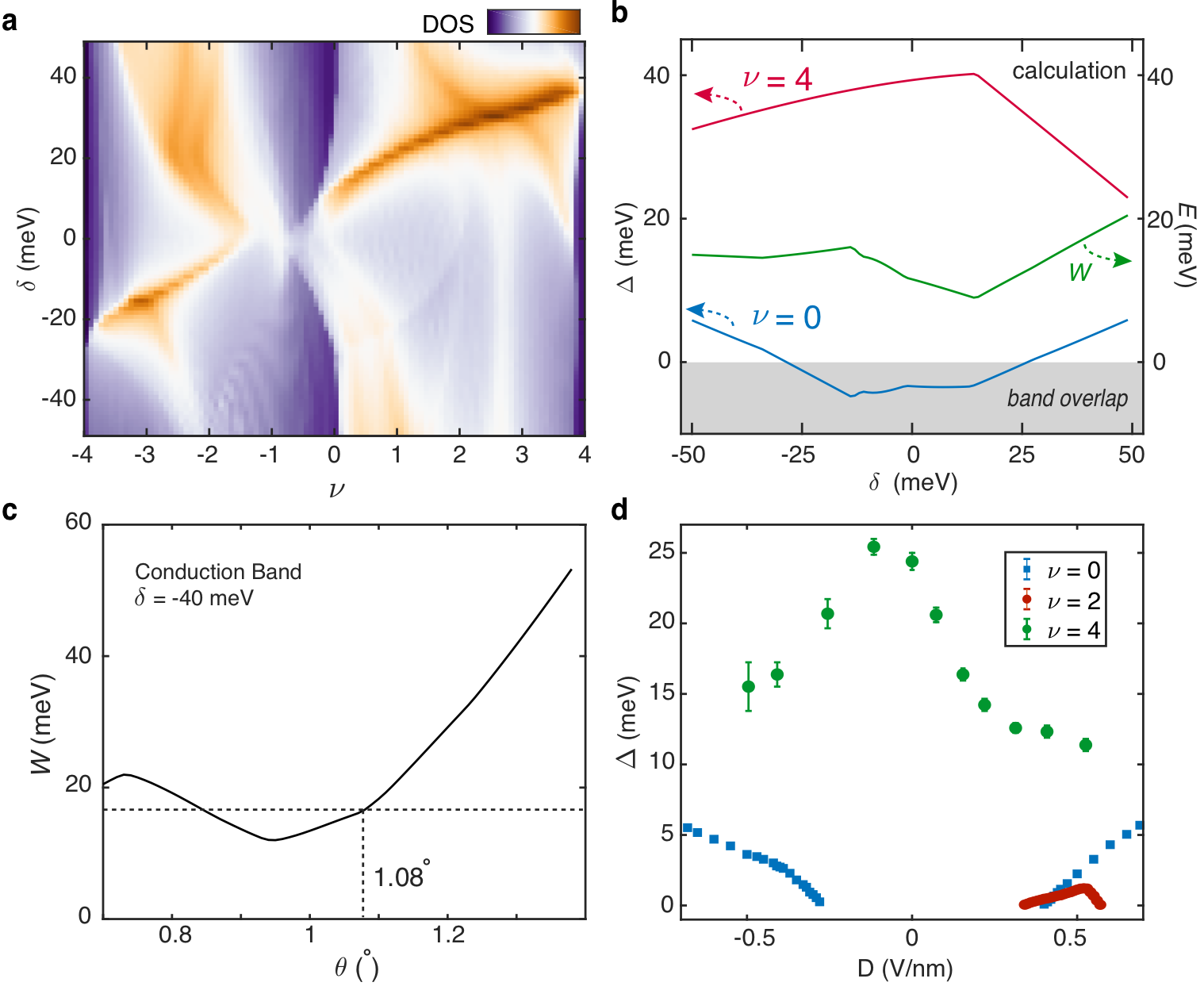
Figure 1b shows the continuum model calculation of the band structure of tMBG at a twist angle of as a function of the interlayer potential difference, (see Supplementary Information). In contrast to tBLG and tDBG, because of the low symmetry the band structure of tMBG differs depending on the direction of (i.e. the sign of ). Additionally, calculations of the layer-resolved local density of states (LDOS) reveal that it is favorable for charge to be arranged highly asymmetrically amongst the three constituent graphene layers. Panels i and ii of Fig. 1c show the LDOS of tMBG calculated at full filling of the conduction band for opposite signs of . In both cases, the moiré potential localizes the LDOS on a triangular lattice of AAB-stacked sites (analogous to AA-stacked sites in tBLG, in which the carbon atoms sit directly atop one another). For (), when the field points from the bilayer towards the monolayer graphene, the LDOS on the outer sheet of the bilayer graphene is suppressed, and the LDOS on the two graphene layers at the rotated interface resembles that of tBLG (panel iii). On the other hand, for (), the LDOS on the outer graphene layer is instead enhanced. In this case the LDOS resembles that of tDBG (panel iv), where the fourth (uppermost) graphene layer has a small LDOS. We would therefore anticipate that tMBG will act similarly to either tBLG or tDBG depending on the sign of , assuming the additional or absent layer of lightly doped graphene plays a limited role.
This picture is borne out well by the experiments. Figure 1d shows the resistivity, , of a tMBG device with (device D1) as a function of carrier density, , and at temperature K. The top axis indicates the filling factor of the bands, (see Methods). Qualitatively, many of the observed features can be associated with the band structure calculated in Fig. 1b (also Supplementary Information Fig. S6). In particular, at the device behaves as a semi-metal for small , but becomes semiconducting at larger . Insulating features are observed over a wide range of at full filling of the conduction or valence band (). Additional resistance peaks disperse as a function of within the flat bands, and likely correspond to van Hove singularities (vHs) as in tDBG He2020 .
In the conduction band (), additional resistive peaks are observed over a finite range of that appear to have no counterparts in the single-particle model. These resistive peaks are observed at integer , each within a different finite range of . Notably, these features are inequivalent for opposite signs of , in contrast with tBLG and tDBG where the correlated states are approximately symmetric with . Measurements of the antisymmetrized Hall coefficient, , provide additional insight into their nature (Fig. 1e). For , there is a highly resistive state at half filling surrounded by a stretched halo of somewhat increased resistance. As in tDBG, changes sign within this extended halo region, suggestive of a spontaneously broken symmetry within the bands He2020 . In contrast, for there are three weakly resistive features at each integer , and abrupt changes in occur only near these features.
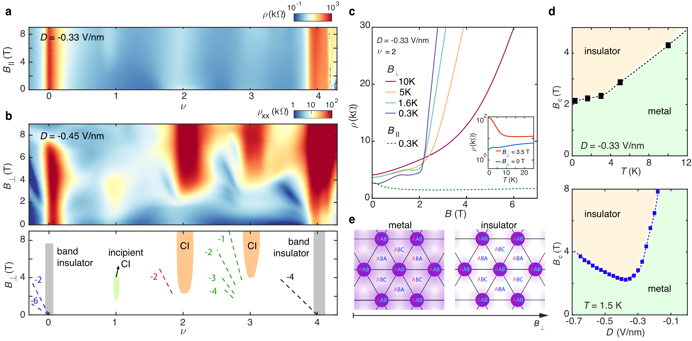
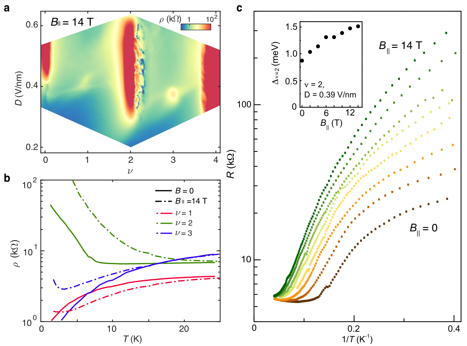
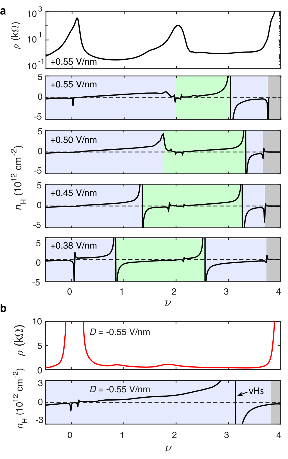
Figure 2a shows the temperature dependence of in the conduction band at V/nm, in which we expect the LDOS distribution to resemble that of tDBG. We observe clear insulating behavior at half filling (), with energy gaps that appear to grow upon applying an in-plane magnetic field indicative of spin-polarized ordering (Supplementary Information Fig. S5). Slightly away from half filling, we observe abrupt drops in as the temperature is lowered (blue curve in the inset of Fig. 2a). These abrupt drops arise within regions of the phase diagram in which the magnitude or sign of the Hall density, , departs from single-particle expectations (green shaded regions in Fig. 2b). These features correspond closely with the CI and metallic states in tDBG Shen2020 ; Liu2019 ; Cao2019 ; Burg2019 ; He2020 , suggesting that at this twist angle the phase diagram of tMBG is similar to that of tDBG, with small differences arising owing to the absence of the weakly charged fourth graphene sheet (see Fig. 1c, iv).
Figure 2c shows similar temperature dependence of at V/nm, in which we expect the LDOS distribution to resemble that of tBLG. The states at all exhibit metallic temperature dependence, defined by a reduction in as is lowered, in direct contrast to the behavior of the CI state for . Notably, the feature at is apparent at high temperature ( K in Fig. 2c), but becomes suppressed at low temperature. Qualitatively similar behavior has been observed previously in tBLG, most clearly in devices with twist angles slightly detuned from the “magic angle” Yankowitz2019 and in devices with strong electrostatic screening from a nearby metal gate Stepanov2019 . This suggests that our devices are marginally correlated compared to magic angle tBLG, potentially owing to a combination of larger bandwidth (Supplementary Information Fig. S6) and electrostatic screening from the addition of the weakly charged third graphene sheet. However, unlike in tBLG, these states can be tuned with . For example, Fig. 2d shows for two values of , in which the state at is apparent at V/nm but not at V/nm. These correlated metallic states are also associated with anomalies in (Fig. 2d); either a sign change (pink shading) or deviations from a linear gate-induced charge density, (gold shading). An additional sign change in is observed for that matches the vHs in the single-particle band structure (see also Supplementary Information Fig. S7), suggesting that correlations do not greatly modify the conduction band Fermi surface at filling factors away from the integers.
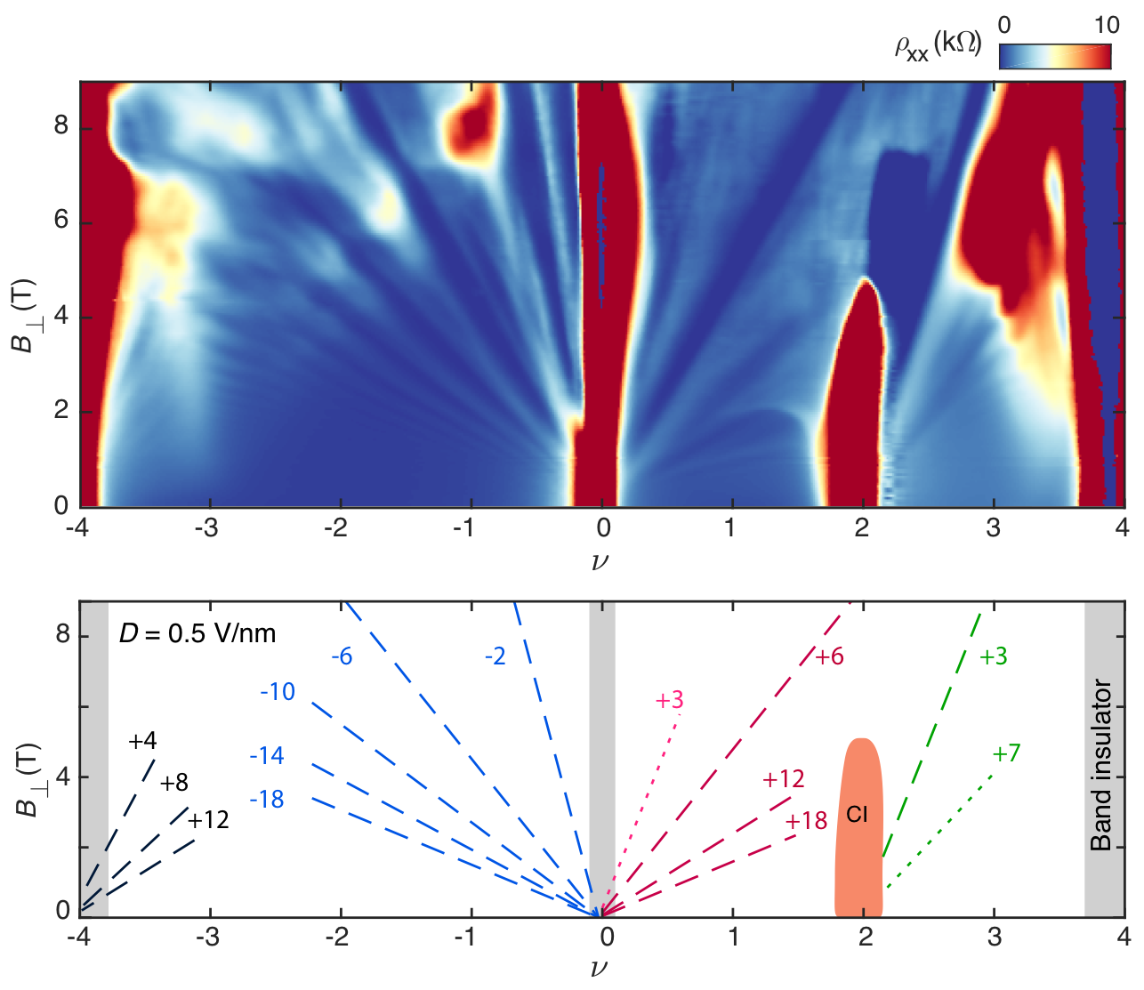
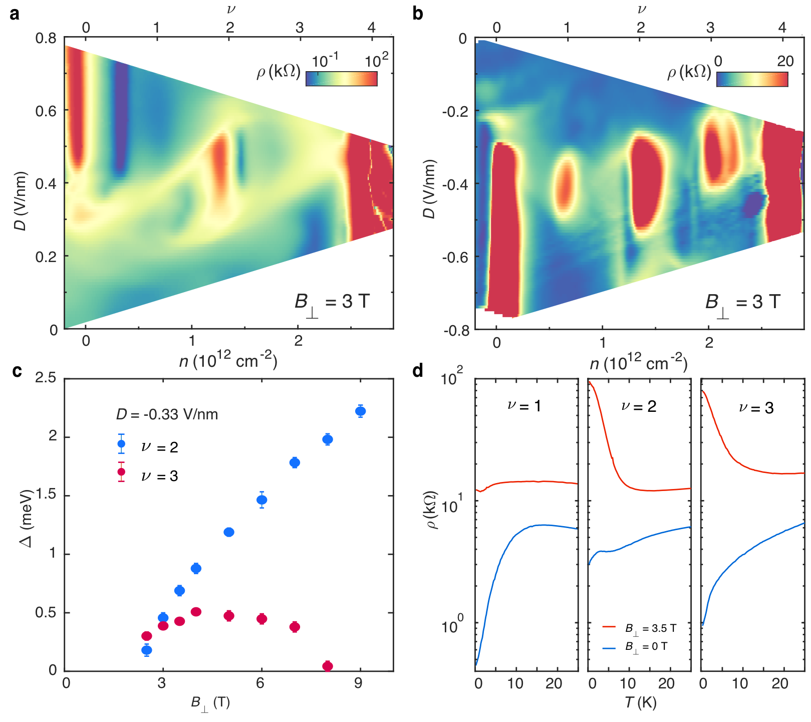
The correlated metallic states observed for have little to no dependence on magnetic field applied in-plane, (shown up to 9 T in Fig. 3a). However, applying a perpendicular field, , causes a sharp transition to an insulating behavior at and 3 above a critical field value (Fig. 3b). Signs of an incipient resistive state can also be seen over a finite range of at . Quantum oscillations associated with the states at and 3 emerge only above a finite , with apparent two-fold degeneracy neighboring and no remaining degeneracies neighboring (Fig. 3b, lower panel). This too is consistent with prior studies of tBLG Yankowitz2019 ; Saito2019 ; Stepanov2019 , in which recent measurements have indicated that a Dirac-like dispersion is revived at each quarter band filling owing to a cascade of spontaneously broken symmetries Zondiner2019 ; Wong2019 .
Figure 3c shows at for various temperatures (solid curves), as well as at K (dashed curve). While is nearly insensitive to , we observe an abrupt transition to insulating behavior above a critical perpendicular magnetic field, , at each temperature, defined as the crossover point between separate linear fits to at low and high . The inset of Figure 3c compares at and 3.5 T for , showing the metallic and insulating behavior, respectively (see Supplementary Information Fig. S8 for ). We find that first grows weakly with increasing temperature, then increases rapidly at higher temperature (Fig. 3d). can also be tuned with , as shown for K in (Fig. 3d). It is peculiar that insulating behavior onsets with but has almost no dependence on . In the simple approximation of a perfectly 2D sample, couples to both the spin and orbital Zeeman energies whereas only couples to the spin Zeeman energy. Consequentially, spin-polarized (unpolarized) states are typically strengthened (suppressed) by a magnetic field pointing in either orientation. The correlated states for do not appear to have a natural interpretation in this context.
Insulating states emerging with have been previously observed in bulk correlated systems including Bechgaard salts Vignolles2005 and high-mobility semiconductors such as Hg1-xCdxTe Rosenbaum1985 ; Field1988 . These insulating states were thought to be driven by orbital confinement effects, associated with spin-density waves in the former and Wigner crystal formation in the latter. The overall similarity of our to those results suggests that related orbital confinement effects may be at play in tMBG. The cartoon schematic in Fig. 3e qualitatively illustrates the presumed atomic-scale electronic structure of tMBG in the metallic and field-assisted insulating phases. The dark purple sites correspond to regions of AAB stacking, and the the lighter pink halo represents the associated LDOS. is expected to orbitally confine the LDOS more tightly around the AAB sites, resulting in an enhancement in the effective interaction strength. In contrast, the LDOS does not depend strongly on as orbital effects are anticipated to be weak owing to the atomically-thin nature of tMBG, and therefore the interaction strength is also not substantially modified.
Qualitatively similar insulating states with associated quantum oscillations have previously been observed to arise abruptly at finite in tBLG devices slightly detuned from the magic angle with strong electrostatic screening from a nearby gate Stepanov2019 . However, the behavior of the states at integer filling with was not reported, therefore a full comparison is not possible. Nevertheless, the overall similarity of these results supports our model of tMBG with as approximately analogous to electrostatically screened tBLG, in which the correlation strength is marginal. One important differnce, however, is that superconductivity appears to be absent in our device, whereas it is a robust ground state in screened tBLG Stepanov2019 ; Saito2019 ; Liu2020 . Differences in bandwidth may be a contributing factor (see Supplementary Information Fig. S6), however it is also possible that the low symmetry of tMBG plays a role. Superconductivity may be sensitive to the combination of Khalaf2020 and symmetries, both broken in tMBG. So far there have been no unambiguous report of superconductivity in a moiré vdW platform with broken symmetry He2020 .
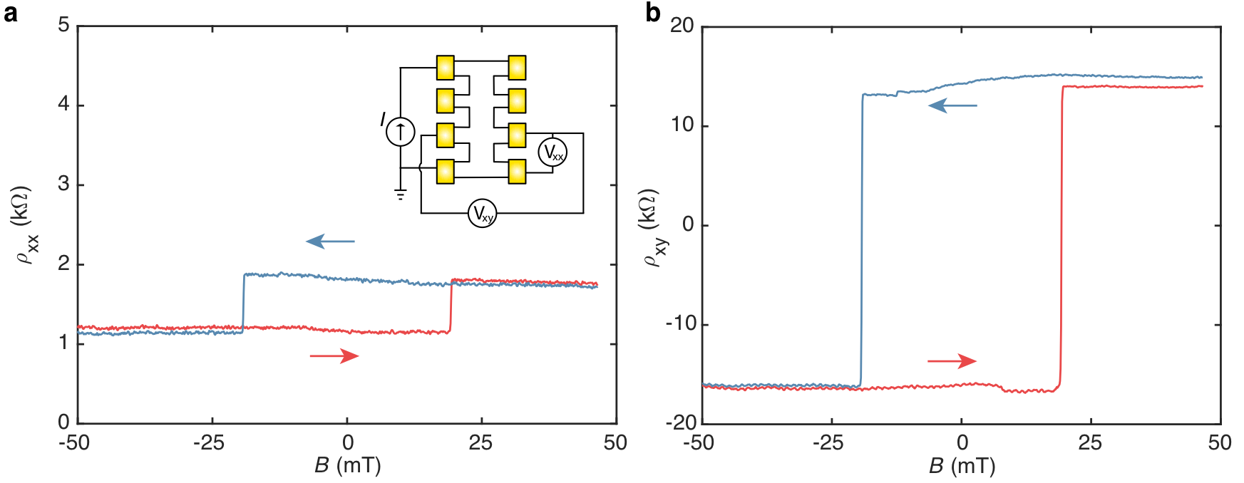
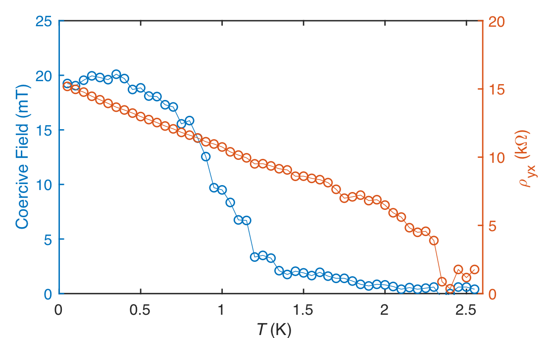
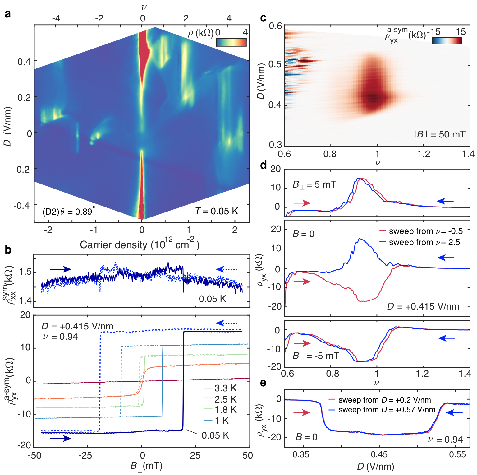
Finally, we turn to the correlated states emerging for in a second device (device D2) which has a slightly smaller twist angle, . Figure 4a shows the resistivity of device D2 at K and T. The overall behavior is similar to device D1, with a few key exceptions. First, the insulating behavior is weak or absent at , indicating the energy gaps to the remote bands are small or zero at this twist angle. Second, incipient CI states can be seen at and for (Supplementary Information Fig. S10), and have no known analog in tDBG. Third, an additional resistive state emerges at over a small range of . Remarkably, this state exhibits a robust anomalous Hall effect (AHE) with large Hall angle at (blue curves in Fig. 4b). exhibits hysteresis about zero magnetic field, an unambiguous characteristic of ferromagnetism. A single loop with a coercive field of mT is formed as the field is swept back and forth. We field symmetrize and antisymmetrize to eliminate small offsets in the two owing to mixing (see Supplementary Information Fig. S9). The temperature dependence of the ferromagnetism is additionally shown in Fig. 4b. The hysteresis and magnitude of the AHE are suppressed upon raising the temperature, and vanish above K (Supplementary Information Fig. S11). The sharpness of the magnetization flip implies that the easy axis is perpendicular to the sample, and that a single magnetic domain is dominant within the measured region of the sample.
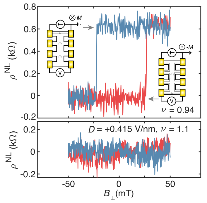
Figure 4c shows a map of antisymmetrized at mT. The regime of ferromagnetic order as a function of and is indicated by the dark red at . The ferromagnetism occurs over an extended range of , and persists into the metallic states slightly outside of the gap. We do not observe any signs of ferromagnetic ordering at any other filling factors in this device. Despite the fact that is not quantized to an integer fraction of , and does not vanish, the large Hall angle indicates transport through edge states. Nonlocal resistance measurements provide further evidence supporting chiral edge conduction in our sample (see Supplementary Information Fig. S12) Kou2014 ; Sharpe2019 . It seems likely that a fully developed Chern insulator state could be realized in a sample with lower disorder or a larger energy gap. In a model of the isolated conduction band of tMBG as four overlapping flat bands with varying spin and valley order, spontaneous polarization of carriers into a single symmetry-broken band with non-zero Chern number, and consequent QAHE, has been predicted Sharpe2019 ; Serlin2020 ; Repellin2019 ; Bultinck2019 ; Zhang2019ahe . However, more exotic ground states with mixed spin and valley polarization may be favored, and our experiment is not sensitive to the exact ground state polarization.
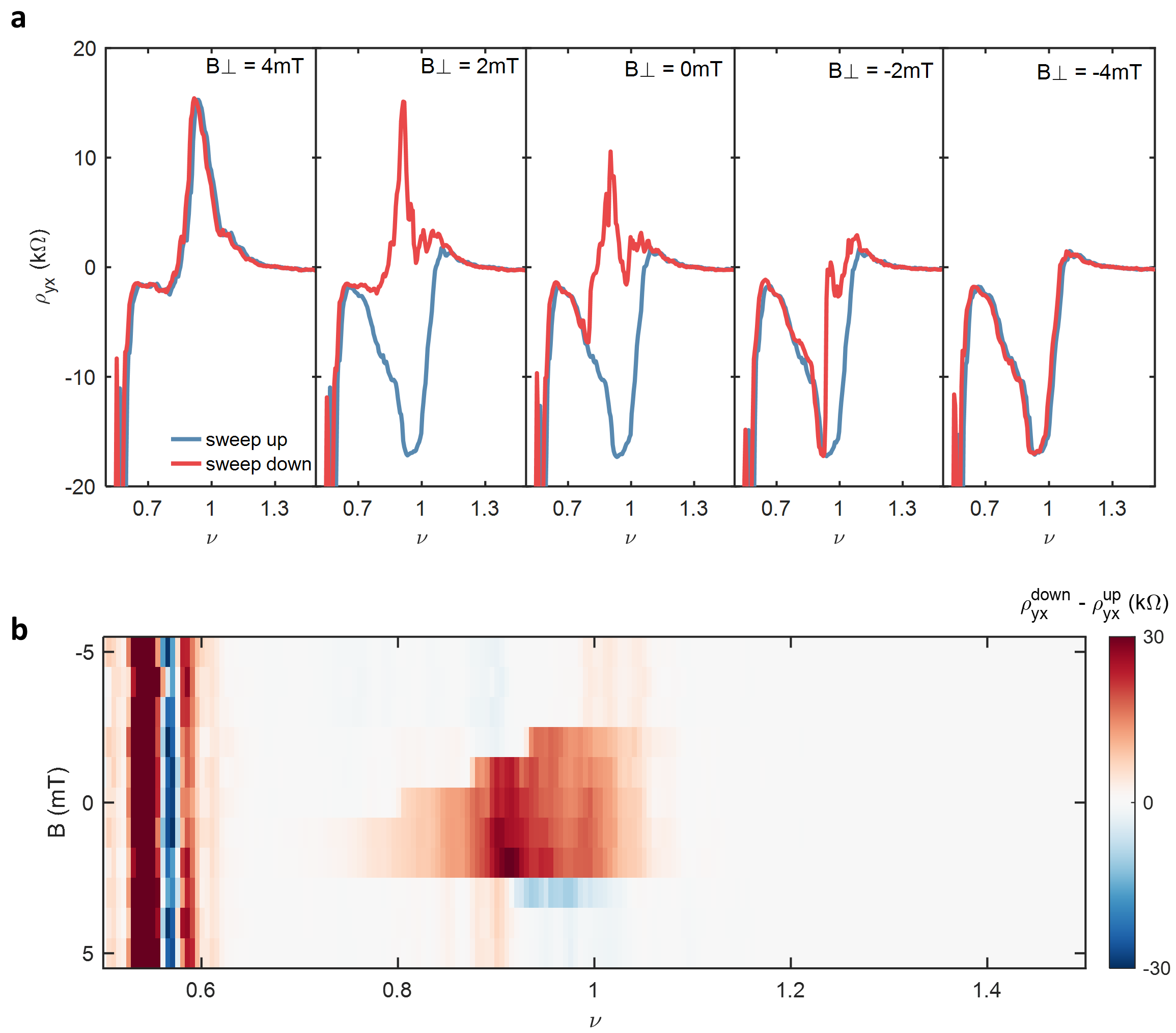
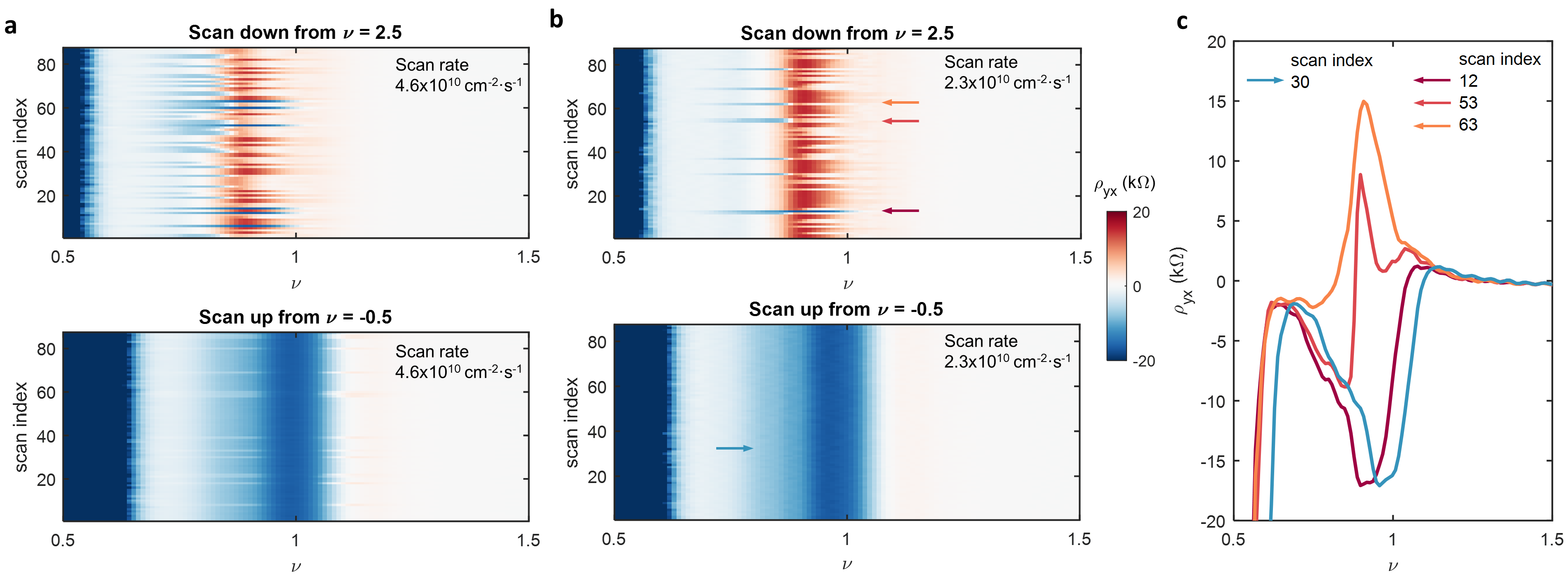
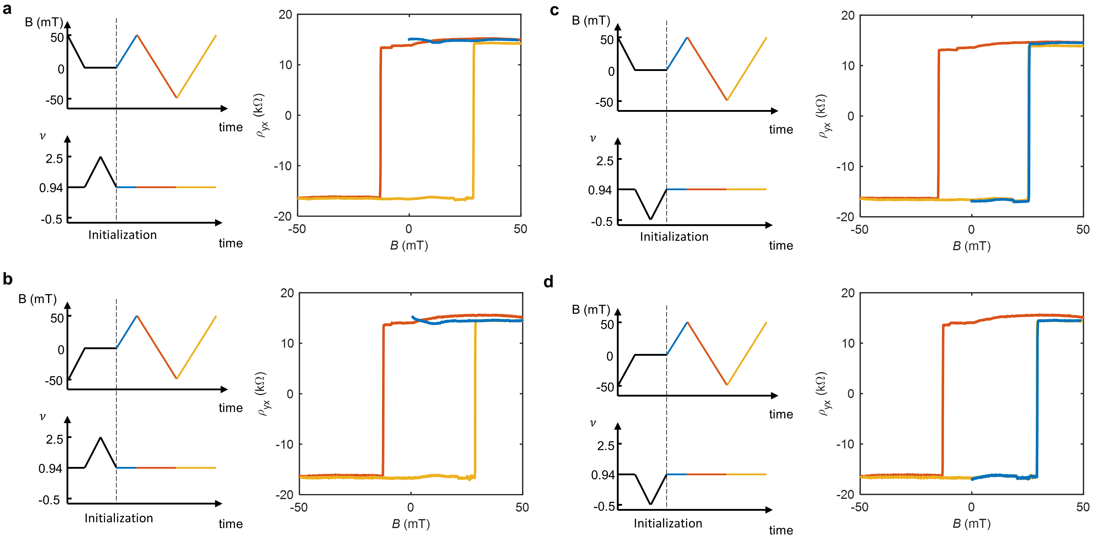
In addition to switching the magnetic ordering with , we are able to control the magnetic state purely with charge doping at . Figure 4d shows as the doping is swept back and forth, exhibiting opposite signs of the magnetic ordering for each sweep direction. In contrast, we do not observe switching upon sweeping back and forth (Figure 4e). Doping-controlled switching of the magnetic order has been recently predicted owing to the unique orbital magnetism exhibited in moiré vdW heterostructures Zhu2020 . However, in contrast to this prediction our switching arises only within a few millitelsa of (Supplementary Information Fig. S13), and therefore likely originates from a different mechanism. Notably, the magnetic order does not switch precisely upon doping across , but rather requires sweeping the doping far away from the magnetically-ordered regime before returning. The switching occasionally occurs through metastable intermediate states and is observed more reliably when is tuned slowly (Supplementary Information Fig. S14), suggesting that it is an intrinsic effect. Furthermore, the switching does not appear to depend on any other initialization conditions (Supplementary Information Fig. S15). Although we are not able to identify the valley and spin ordering of the surrounding symmetry-broken bands at , this effect appears to be tied to a selective polarization of each of these bands with doping. The exact mechanism responsible for these unusual switching dynamics — including whether it is of fundamental origin or related to sample inhomogeneity — remains an open question for future work.
The ability to electrically switch magnetic order is rare amongst known materials, and can typically be achieved with electric fields only in multiferroics Matsukura2015 . tMBG therefore provides a new platform for spintronics applications with purely doping-controlled magnetism and ultra-low power dissipation. More generally, our results demonstrate that the low symmetry of tMBG enables a wide array of highly tunable correlated states which differ upon changing the sign of . The addition of intrinsic non-trivial band topology also raises the possibility of realizing fractional Chern insulator states Zhang2019 in samples with stronger correlations at different twist angle or under pressure Yankowitz2019 . We anticipate that tMBG will be a crucial platform for further understanding of these correlated and topological states of matter, providing unprecedented control with external tuning parameters.
Methods
tMBG devices are fabricated using the “cut-and-stack” method Saito2019 . We identify exfoliated graphene flakes with regions of both monolayer and bilayer graphene, and use an atomic force microscope (AFM) tip to isolate a region from each area Chen2019 ; Saito2019 . We find that in general, longer AFM-cut edges can increase the friction between rotated graphene sheets and improve the yield of devices near the targeted twist angle. Samples are assembled using a standard dry transfer technique that utilizes a polycarbonate (PC) film on top of a polydimethyl siloxane (PDMS) dome wang_one-dimensional_2013 . Completed heterostructures are transferred onto a Si/SiO2 wafer. The temperature is kept below 180∘C during device fabrication to preserve the intended twist angle.
All devices are encapsulated between flakes of BN with typical thickness of nm, and have graphite top and bottom gates (except the device with twist angle of 1.44∘, which has a silicon bottom gate). In devices with a graphite bottom gate, a gate voltage is applied to the Si gate in order to dope the region of the graphene contacts overhanging the graphite back gate to a high charge carrier density and reduce the contact resistance. and can be tuned by the gate voltages through the relation , , where () is the capacitance between the top (bottom) gate and tMBG, and is the electron charge. We choose a convention such that corresponds to the field pointing from from monolayer to bilayer graphene.
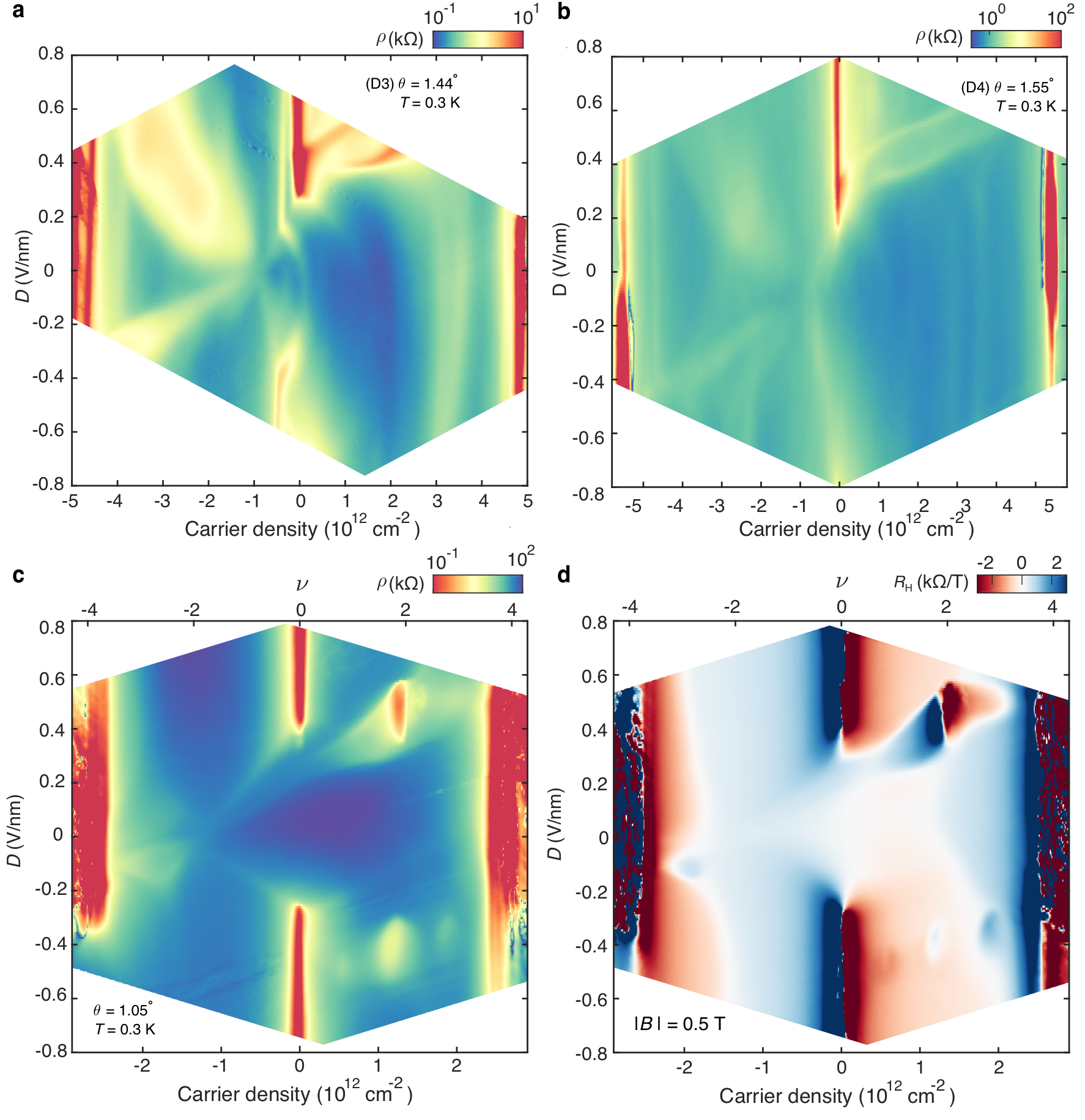
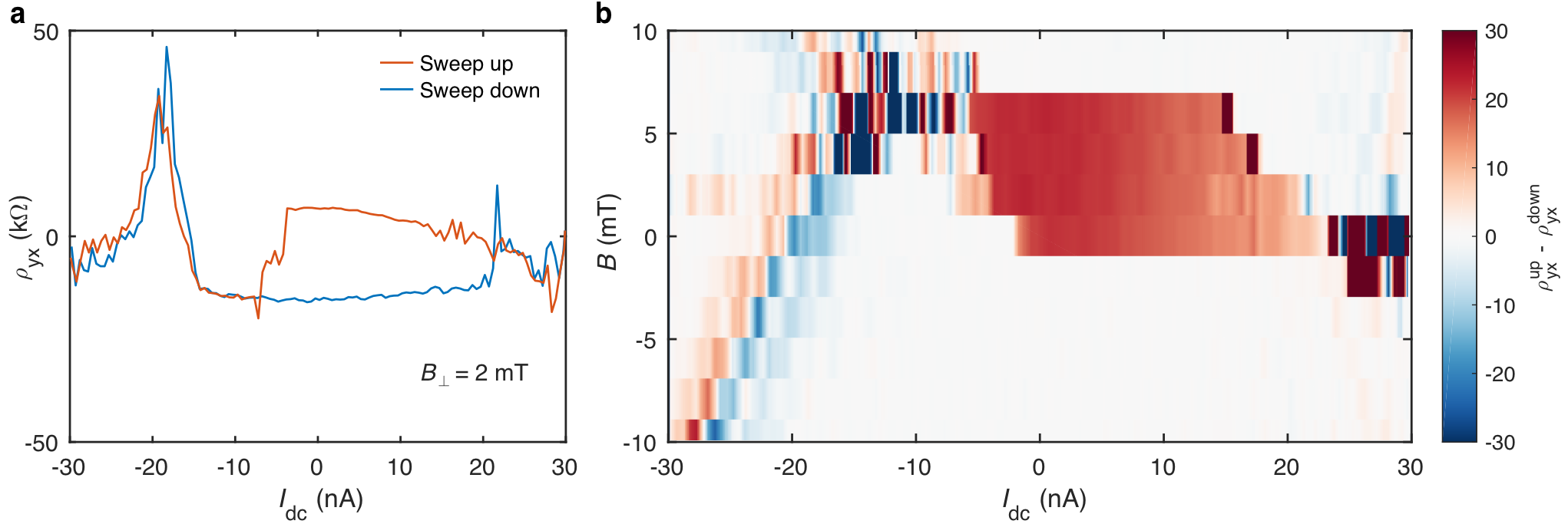
We measure electrical transport in four tMBG devices with twist angles varying between and 1.55∘ (Supplementary Information Figs. S1, S2, and S3). Transport measurements are conducted in a four-terminal geometry with ac current excitation of nA using standard lock-in techniques at either 13.3 Hz or 17.7 Hz. The magnetic hysteresis loops in device D2 are measured using a 500 pA excitation. A dc current bias, , can additionally be added to further control the magnetic state (Supplementary Information Fig. S16), as has been discussed previously in devices of tBLG aligned with BN Sharpe2019 ; Serlin2020 .
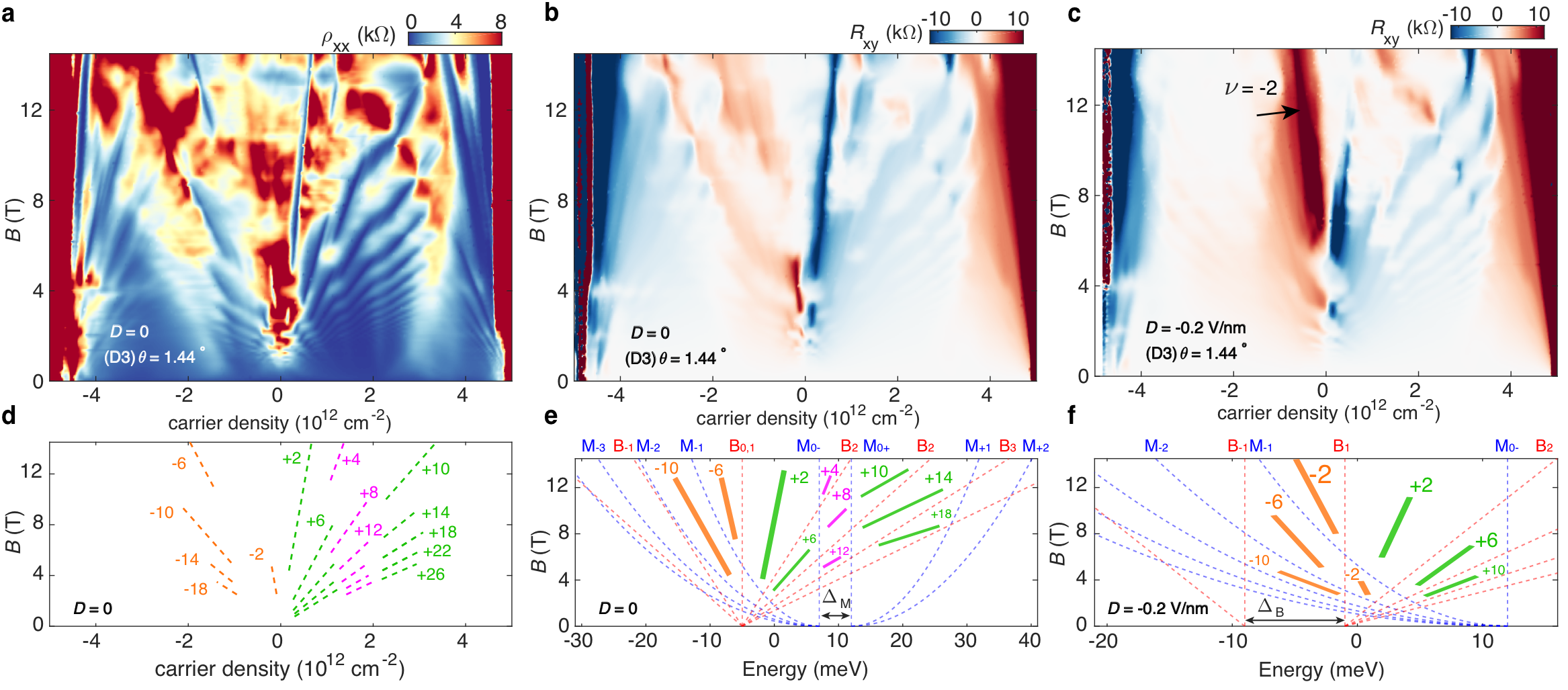
The twist angle is determined from the values of charge carrier density at which the insulating states at are observed, following , where nm is the lattice constant of graphene. The values of are determined from the sequence of quantum oscillations in a magnetic field which project to (or for , see Supplementary Information Fig. S4.).
acknowledgments
We thank A. Young, H. Polshyn, A. Millis, C.-Z. Chang, J.-H. Chu, and E. Khalaf for helpful discussions. Research on correlated states in twisted monolayer-bilayer graphene was primarily supported as part of Programmable Quantum Materials, an Energy Frontier Research Center funded by the U.S. Department of Energy (DOE), Office of Science, Basic Energy Sciences (BES), under award DE-SC0019443. Measurements and understanding of ferromagnetism at the University of Washington were partially supported by NSF MRSEC 1719797. X.X. acknowledges support from the Boeing Distinguished Professorship in Physics. X.X. and M.Y. acknowledge support from the State of Washington funded Clean Energy Institute. This work made use of a dilution refrigerator system which was provided by NSF DMR-1725221. K.W. and T.T. acknowledge support from the Elemental Strategy Initiative conducted by the MEXT, Japan and the CREST (JPMJCR15F3), JST.
Author contributions
S.C., M.H. and V.H. fabricated the devices and performed the measurements. Y.-H. Z. performed the calculations. Z.F. and D.H.C. assisted with measurements in the dilution refrigerator. K.W. and T.T. grew the BN crystals. S.C., M.H., X.X., C.R.D. and M.Y. analyzed the data and wrote the paper with input from all authors.
Competing interests
The authors declare no competing interests.
Data availability
The data that support the plots within this paper and other findings of this study are available from the corresponding author upon reasonable request.
References
- (1) Cao, Y. et al. Correlated insulator behaviour at half-filling in magic-angle graphene superlattices. Nature 556, 80–84 (2018).
- (2) Cao, Y. et al. Unconventional superconductivity in magic-angle graphene superlattices. Nature 556, 43–50 (2018).
- (3) Yankowitz, M. et al. Tuning superconductivity in twisted bilayer graphene. Science 363, 1059–1064 (2019).
- (4) Lu, X. et al. Superconductors, orbital magnets, and correlated states in magic angle bilayer graphene. Nature 574, 653–657 (2019).
- (5) Stepanov, P. et al. The interplay of insulating and superconducting orders in magic-angle graphene bilayers. arXiv:1911.09198 (2019).
- (6) Saito, Y., Ge, J., Watanabe, K., Taniguchi, T. & Young, A. F. Decoupling superconductivity and correlated insulators in twisted bilayer graphene. arXiv:1911.13302 (2019).
- (7) Sharpe, A. L. et al. Emergent ferromagnetism near three-quarters filling in twisted bilayer graphene. Science 365, 605–608 (2019).
- (8) Serlin, M. et al. Intrinsic quantized anomalous Hall effect in a moiré heterostructure. Science 367, 900–903 (2020).
- (9) Arora, H. S. et al. Superconductivity without insulating states in twisted bilayer graphene stabilized by monolayer WSe2. arXiv:2002.03003 (2020).
- (10) Shen, C. et al. Correlated states in twisted double bilayer graphene. Nature Physics DOI:10.1038/s41567–020–0825–9 (2020).
- (11) Liu, X. et al. Spin-polarized Correlated Insulator and Superconductor in Twisted Double Bilayer Graphene. arXiv:1903.08130 (2019).
- (12) Cao, Y. et al. Electric Field Tunable Correlated States and Magnetic Phase Transitions in Twisted Bilayer-Bilayer Graphene. arXiv:1903.08596 (2019).
- (13) Burg, G. W. et al. Correlated Insulating States in Twisted Double Bilayer Graphene. Physical Review Letters 123, 1–7 (2019).
- (14) He, M. et al. Tunable correlation-driven symmetry breaking in twisted double bilayer graphene. arXiv:2002.08904 (2020).
- (15) Chen, G. et al. Evidence of a gate-tunable mott insulator in trilayer graphene moiré superlattice. Nature Physics 15, 237–241 (2019).
- (16) Chen, G. et al. Signatures of tunable superconductivity in a trilayer graphene moiré superlattice. Nature 572, 215–219 (2019).
- (17) Chen, G. et al. Tunable correlated Chern insulator and ferromagnetism in a moiré superlattice. Nature 579, 56–61 (2020).
- (18) Tang, Y. et al. Simulation of Hubbard model physics in WSe2/WS2 moiré superlattices. Nature 579, 353–358 (2020).
- (19) Regan, E. C. et al. Mott and generalized Wigner crystal states in WSe2/WS2 moiré superlattices. Nature 579, 359–363 (2020). eprint 1910.09047.
- (20) Wang, L. et al. Magic continuum in twisted bilayer WSe2. arXiv:1910.12147 (2019).
- (21) Suárez Morell, E., Pacheco, M., Chico, L. & Brey, L. Electronic properties of twisted trilayer graphene. Phys. Rev. B 87, 1–7 (2013).
- (22) Ma, Z. et al. Topological flat bands in twisted trilayer graphene. arXiv:1905.00622 (2019).
- (23) Liu, J., Ma, Z., Gao, J. & Dai, X. Quantum valley hall effect, orbital magnetism, and anomalous hall effect in twisted multilayer graphene systems. Phys. Rev. X 9, 031021 (2019).
- (24) Zondiner, U. et al. Cascade of Phase Transitions and Dirac Revivals in Magic Angle Graphene. arXiv:1912.06150 (2019).
- (25) Wong, D. et al. Cascade of transitions between the correlated electronic states of magic-angle twisted bilayer graphene. arXiv:1912.06145 (2019).
- (26) Vignolles, D. et al. Field-induced spin-density wave in . Phys. Rev. B 71, 020404 (2005).
- (27) Rosenbaum, T., Field, S., Nelson, D. & Littlewood, P. Magnetic-field-induced localization transition in hgcdte. Phys. Rev. Lett. 54, 241–244 (1985).
- (28) Field, S., Reich, D. H., Rosenbaum, T., Littlewood, P. & Nelson, D. Electron correlation and disorder in in a magnetic field. Phys. Rev. B 38, 1856 (1988).
- (29) Liu, X. et al. Tuning electron correlation in magic-angle twisted bilayer graphene using coulomb screening. arXiv:2003.11072 (2020).
- (30) Khalaf, E., Chatterjee, S., Bultinck, N., Zaletel, M. P. & Vishwanath, A. Charged skyrmions and topological origin of superconductivity in magic angle graphene. arXiv:2004.00638 (2020).
- (31) Kou, X. et al. Scale-invariant quantum anomalous hall effect in magnetic topological insulators beyond the two-dimensional limit. Phys. Rev. Lett. 113, 137201 (2014).
- (32) Repellin, C., Dong, Z., Zhang, Y.-H. & Senthil, T. Ferromagnetism in narrow bands of moiré superlattices. arXiv:1907.11723 (2019).
- (33) Bultinck, N., Chatterjee, S. & Zaletel, M. P. Anomalous Hall ferromagnetism in twisted bilayer graphene. arXiv:1901.08110 (2019).
- (34) Zhang, Y.-H., Mao, D. & Senthil, T. Twisted bilayer graphene aligned with hexagonal boron nitride: Anomalous Hall effect and a lattice model. Physical Review Research 1, 033126 (2019).
- (35) Zhu, J., Su, J.-J. & MacDonald, A. H. The curious magnetic properties of orbital chern insulators. arXiv:2001.05084 (2020).
- (36) Matsukura, F., Yokura, Y. & Ohno, H. Control of magnetism by electric fields. Nature Nanotechnology 10, 209–220 (2015).
- (37) Zhang, Y.-H., Mao, D., Cao, Y., Jarillo-Herrero, P. & Senthil, T. Nearly flat chern bands in moiré superlattices. Phys. Rev. B 075127, 075127 (2019).
- (38) Wang, L. et al. One-Dimensional Electrical Contact to a Two-Dimensional Material. Science 342, 614–617 (2013).
- (39) Lee, J. Y. et al. Theory of correlated insulating behaviour and spin-triplet superconductivity in twisted double bilayer graphene. Nature Communications 10, 1–10 (2019). eprint 1903.08685.
Supplementary Information
S1 Calculation of Band Structure
We calculate the band structure using the standard continuum model. The Hamiltonian is
| (S1) |
We have
| (S2) |
where with as the twist angle. is the transformation matrix for anticlockwise rotation with angle .
The Hamiltonian for the bilayer graphene is
| (S3) |
where and .
Finally the inter-layer moiré tunneling term is
| (S4) |
where , and , with as the moiré lattice constant.
Here and are electron operators for the monolayer graphene and the bilayer graphene respectively. We use parameters meV. For the inter-layer tunning, we use meV and . is a sublattice potential term for the monolayer graphene which may originate from hBN alignment. We use meV. is the potential difference which is tuned by the displacement field .
With sufficient , the neutrality gap is opened and we can define valley Chern number for the conduction and valence bands. Here we focus on the conduction band, the valley Chern number is and for and sides respectively.

