Growth and Characterization of Homoepitaxial -Ga2O3 Layers
Abstract
-Ga2O3 is a next-generation ultra wide bandgap semiconductor (Eg = ) that can be homoepitaxially grown on commercial substrates, enabling next-generation power electronic devices among other important applications. Analyzing the quality of deposited homoepitaxial layers used in such devices is challenging, in part due to the large probing depth in traditional x-ray diffraction (XRD) and also due to the surface-sensitive nature of atomic force microscopy (AFM). Here, a combination of evanescent grazing-incidence skew asymmetric XRD and AFM are investigated as an approach to effectively characterize the quality of homoepitaxial -Ga2O3 layers grown by molecular beam epitaxy at a variety of Ga/O flux ratios. Accounting for both structure and morphology, optimal films are achieved at a Ga/O ratio of 1.15, a conclusion that would not be possible to achieve by either XRD or AFM methods alone. Finally, fabricated Schottky barrier diodes with thicker homoepitaxial layers are characterized by J-V and C-V measurements, revealing an unintentional doping density of - in the epilayer. These results demonstrate the importance of complementary measurement methods for improving the quality of the -Ga2O3 homoepitaxial layers used in power electronic and other devices.
Keywords: Molecular Beam Epitaxy, Gallium Oxide, X-ray diffraction, Atomic Force Microscopy, Schottky Diode
1 Introduction
-Ga2O3 is a promising ultra wide band gap semiconductor[1, 2], featuring 4.8 - 4.9 eV bandgap[3, 4], controllable n-type doping with group IV elements (Si, Ge, Sn)[5, 6, 7], and a large-size low-cost[8] bulk single crystal substrate wafers[9, 10]. Because of these properties, -Ga2O3 and related alloys[11] are studied for solar-blind ultraviolet (UV) photodetectors[12], high-power and radio-frequency electronic devices [13, 14], high-temperature gas sensors[15] and other potential applications[16]. In the field of -Ga2O3 power electronic applications, research activities have rapidly advanced over the past decade leading to improved device performance[17, 18, 19]. For example, vertical and trench Schottky barrier diodes have been achieved with a Baliga’s figure of merit (BFOM) approaching 1 [20, 21], and vertical field effect transistors with breakdown voltage 1 and on-state resistance of have been demonstrated[22, 23]. However, there are remaining and well-founded concerns regarding the low thermal conductivity[24, 25] and lack of p-type dopability of -Ga2O3[26, 27], which would have to be addressed for future power electronic device applications.
Despite the advances in -Ga2O3 device fabrication technology, routine characterization of homoepitaxial layer quality is complicated due to difficulty in discriminating between the substrate and the epilayer. This has been especially challenging when studying thin epitaxial layers in complex multi-layer device structures. Conventional x-ray diffraction (XRD) scans are routinely performed, but their analysis is limited to determining the layer thickness from Pendellösung interference fringes[28]. XRD rocking curves are commonly measured, but the full width at half maximum (FWHM) is dominated by the signal from the substrate[29]. Other commonly used method are sensitive only to the surface quality of the homoepitaxial layer, like reflection high energy electron diffraction (RHEED)[7, 28] or atomic force microscopy (AFM)[7, 30]. In-plane grazing incidence X-ray diffraction (GIXD) is a useful method to evaluate homoepitaxial layer quality[31, 27], however this technique requires a specialized diffractometer with an in-plane arm that is not as widely available to the scientific community as a standard 4-circle x-ray diffractometer. X-ray topography is another method capable of characterizing homoepitaxial layers, however it requires access to a synchotron radiation facility[32].
Here, we explore skew asymmetric X-ray diffraction (XRD) at grazing incidence angles as a method to quantify -Ga2O3 homoepitaxial layer crystal quality. This method is more broadly accessible to the scientific community than GIXD through the use of a standard 4-circle diffractometer. The skew asymmetric XRD results are correlated with changes in surface morphology as measured by atomic force microscopy (AFM) across a wide range of Molecular Beam Epitaxy (MBE) growth conditions to determine optimal growth parameters. Secondary Ion Mass Spectrometry (SIMS) is used to verify the chemical purity of the epilayers and their thickness, obtained from fitting of interference fringes in XRD scans to determine a growth rate curve. Finally, thicker homoepitaxial layers processed into vertical Schottky diodes are characterized by current - voltage measurements to verify the blocking characteristics of the homoepitaxial layer, and by capacitance - voltage measurements to determine the effective background electron concentration of the epilayer. Together, these results present a broader view of the role that growth stoichiometry plays in homoepitaxial layer quality.
2 Experimental Methods
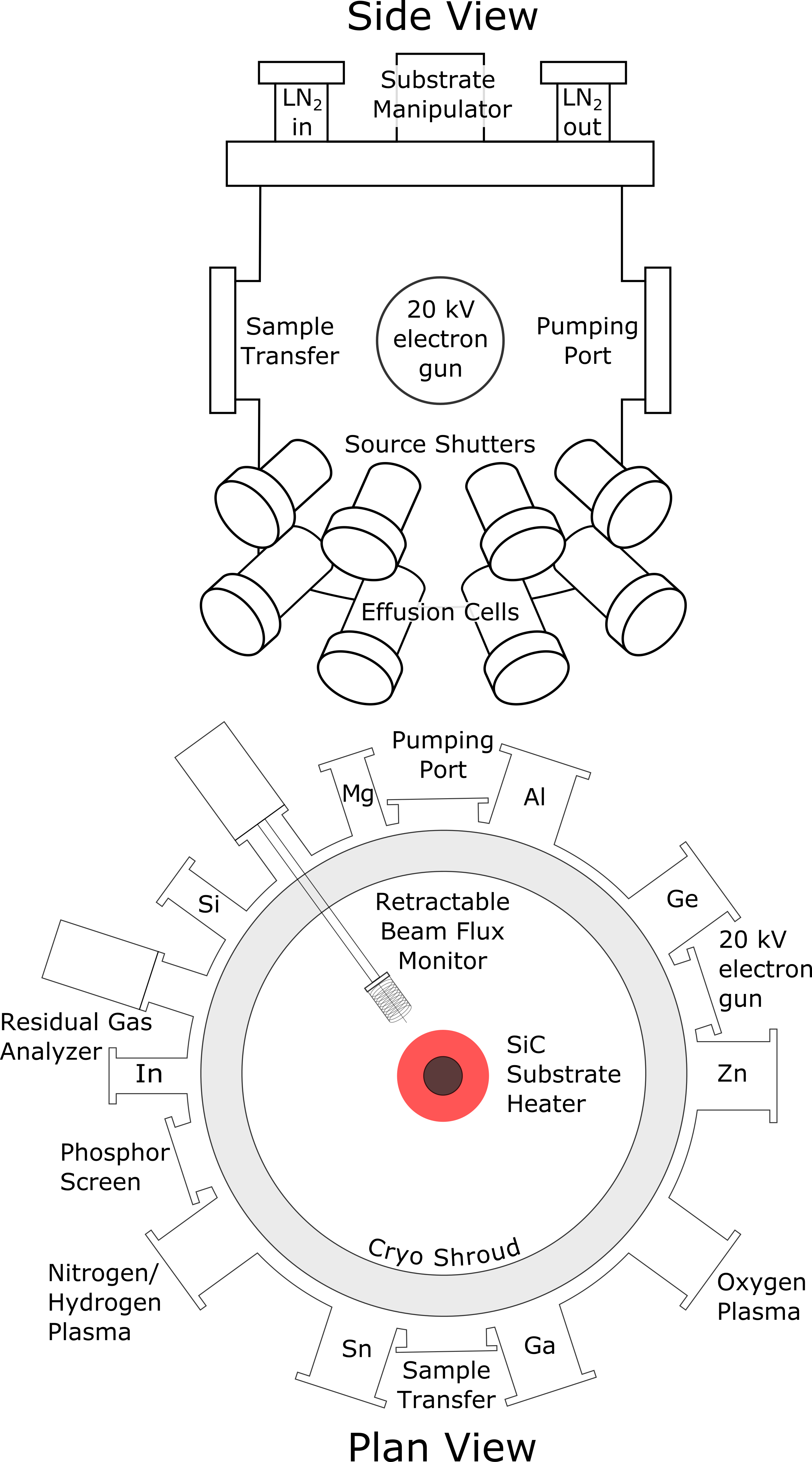
-Ga2O3 was grown homoepitaxially on (010) and (01) oriented 10 x 15 wafers (Tamura Corporation) using a Riber Compact 21T molecular beam epitaxy (MBE) deposition system which is schematically depicted in Figure 1. Substrates were cleaned by a sequential solvent rinse of acetone/methanol/2-propanol followed by a deionized (DI) water rinse. The substrates were then indium bonded to Si carrier wafers to absorb IR radiation from the substrate heater. 7N Ga was sourced from a SUMO style effusion cell, and high purity dry oxygen (SAES purifier, 1 part per billion H2O by volume) was supplied through a 13.56 radio-frequency oxygen plasma source operating at 300 with flows of 2.0 SCCM - 3.0 SCCM. Substrates were outgassed in an introductory vacuum chamber at 150 for 90 minutes before transferring to an intermediate holding chamber. Before growth, Ga fluxes were measured using a Bayard-Alpert style retractable ionization gauge. All substrates were annealed at 800 , while exposed to an oxygen plasma operated at 300 W and 2.0 SCCM, for 30 minutes before growth. All films were grown at a substrate temperature of 700 as measured by a thermocouple on the opposite side of the carrier wafer, resulting in film thickness in the 100 nm range. Detailed film thicknesses can be found in the Supporting Information, Table 1. Films were analyzed in situ by reflection high energy diffraction (RHEED).
XRD was performed using a Rigaku Smartlab diffractometer using Cu-K radiation monochromated by a 4-bounce Ge-(220) crystal, and a Panalytical MRD Pro using Cu-K- radiation with a hybrid monochromator (Göbel mirror plus a 4-bounce Ge-(400) crystal) on the incident beam. A Veeco/Bruker D3100, with a Nanoscope 5 controller unit, was used to collect AFM images. Measurements were conducted tapping mode with a 20 at a scan rate of 0.35 , and the samples were secured using a vacuum stage. Post processing of images included flattening with a 3rd order function and a denoise algorithm.
An ION-TOF TOF-SIMS V Time of Flight SIMS (TOF-SIMS) spectrometer was utilized for depth profiling. Analysis was completed utilizing a 3-lens 30 BiMn primary ion gun. Depth profiles were completed with the 30 Bi+ primary ion beam, (0.8 pulsed beam current), a 50 50 area was analyzed with a 256:256 pixel primary beam raster. Sputter depth profiling for positive ion yield was accomplished with 3 oxygen ion sputter beam (30 sputter current) with a raster of . Sputter depth profiling for negative ion yield was accomplished with 3 cesium ion sputter beam (34 sputter current) with a raster of .
Schottky contacts were deposited on thicker ( 500 nm) MBE-grown -Ga2O3 on Sn-doped () oriented substrates, and Ohmic contacts were deposited on the backside of the wafers to form vertical Schottky diodes. Post-growth, the wafers were cleaned via a rinse in 30% hydrochloric acid (HCl) to remove the indium from the backside. Wafers were then cleaned with a quick succession of rinses in acetone, 2-propanol, and DI water, which was then dried with N2. Samples were then rinsed once again in 30 % HCl, DI water, and dried with N2 to prepare the backside surface for the ohmic contact. The backside ohmic contact, consisting of Ti(20 )/Au(100 ) was deposited by e-beam evaporation. Samples were then processed via rapid thermal annealing (RTA) in N2 at 400 for 1 minute. A second clean of acetone, 2-propanol, and DI water, and dry N2 was used prior to the e-beam evaporation of the Pt(50 )/Ti(10 )/Au(100 ) circular Schottky contacts, which were defined by a shadow mask.
The Schottky diode characteristics were measured using a Keithley 4200A-SCS parameter analyzer. Current-Voltage (J-V) data was taken in two steps, with the voltage scanned from and the current compliance set at 100 . The on-off ratio, turn-on voltage, ideality factor, and on-state resistance were determined by fitting portions of the J-V curves to diode equation. The Capacitance-Voltage (C-V) data was taken at a frequency of 1 , over a voltage range from . The carrier concentration was determined from C-V using Mott-Schottky analysis at negative voltages where the capacitance was not limited by turn on of the diode. Analysis of the depletion width was limited to 380 nm by the applied DC bias. To prepare the data points for differential analysis (d(1/C2)/dV) the data was smoothed using a piecewise Savitsky-Golay filter of order 2, kernel 3 for 1 V 1.5 and order 3, kernel 11 for the remaining data.
3 Results and Discussion
3.1 Film Growth
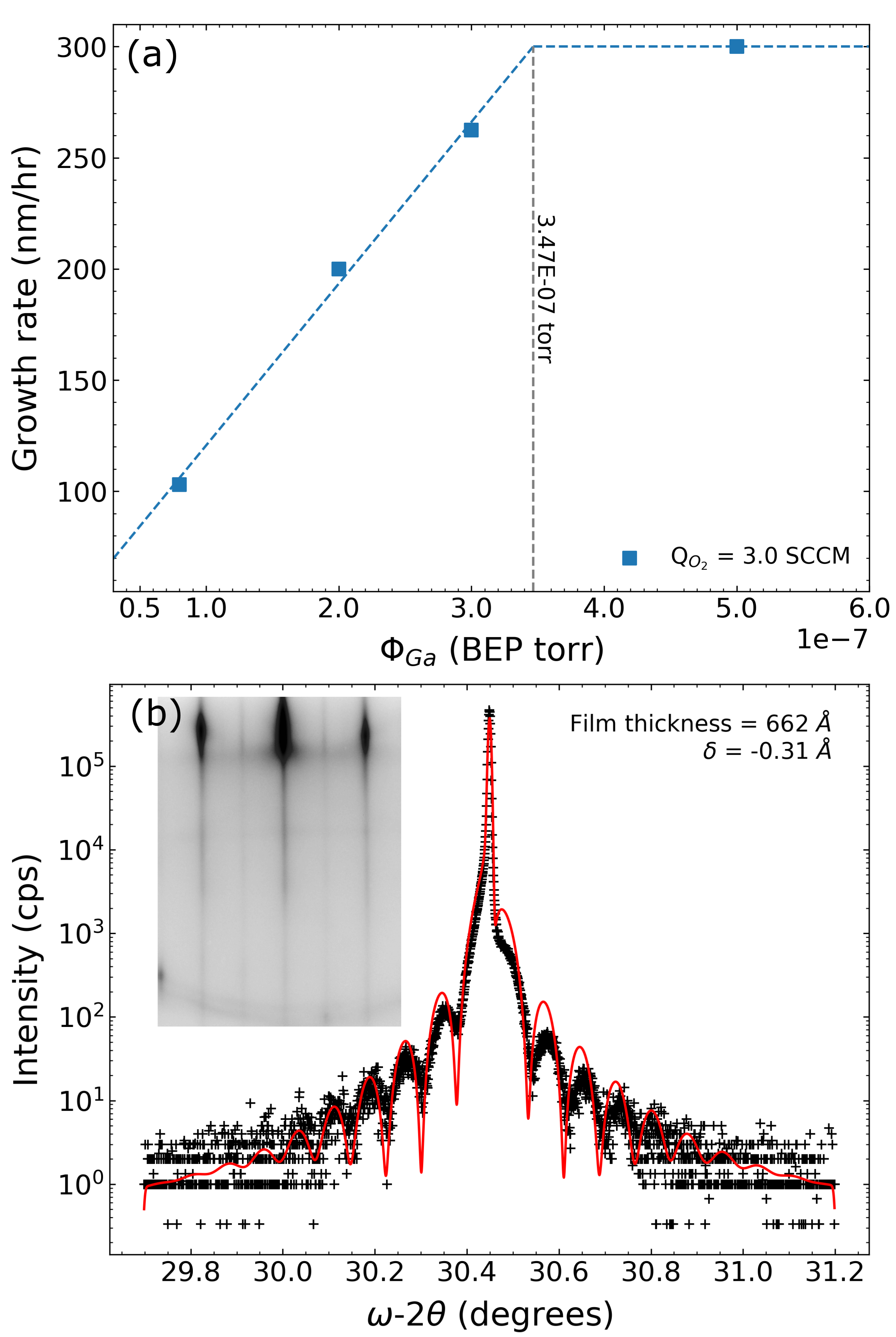
To establish growth regimes and the stoichiometric growth rate, -Ga2O3 films were initially grown at varying incident Ga fluxes. Using plasma conditions of 3.0 SCCM O2 and 300 , the stoichiometric oxygen flux was determined to be 300 nm/hr, corresponding to a Ga beam equivalent pressure (BEP) of . This trend is shown in Figure 2 (a), and is well aligned with the growth regimes previously reported for -Ga2O3[28, 17]. All film thicknesses were determined by analysis of Pendellösung thickness fringes, as shown in Figure 2 (b). While a perfect homoepitaxial film should not show these fringes, it has been well documented that a slight interface offset, , is responsible for the appearance of these fringes[28, 33]. For the fit, instrument broadening is accounted for using a convolved gaussian, and fringe decay is modeled by surface roughness using a gaussian envelope. Films were also monitored in situ by RHEED, and a representative pattern perpendicular to the 001 azimuth is shown in the inset of Figure 2 (b) indicating a smooth and high quality surface by the streaky nature of the pattern and the appearance of a 2 surface reconstruction, visible as a half order streak between the primary streaks.
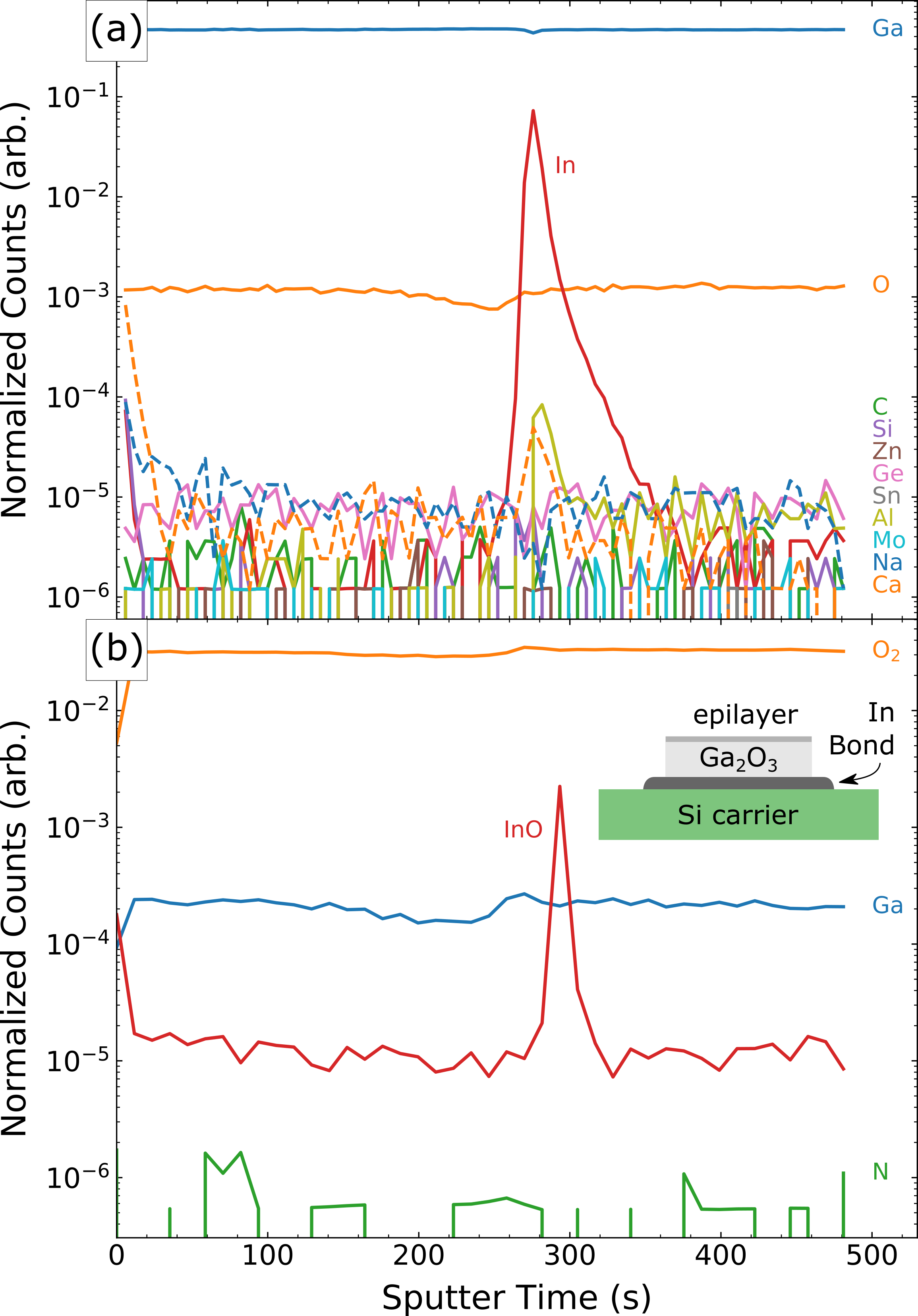
SIMS depth profiles were performed to investigate the origin of the interfacial offset resulting in the thickness fringes described above. Additionally, the MBE chamber used to deposit -Ga2O3 films is also used to deposit other semiconductor materials, and SIMS can be used to analyze epilayers for these contaminants at impurity concentrations. Namely, the chamber contains Si, Al, Ge, Zn, In, Sn, O and N (see Figure 1). Mo blocks are also used to hold the Si carrier wafers in the chamber which could provide an additional source of contamination through the formation of volatile MoO3[34]. Figure 3 (a) shows a SIMS depth profile analyzing positively charged ions highlighted above along with other common impurities including C and Na. Nitrogen was interrogated by a separate depth profile analyzing negative ions, shown in Figure 3 (b). All bulk impurities, including Zn and O, were below the detection limit in the epilayer; however, contamination was observed at the homoepitaxial interface. In, Al, and Ca are observed to spike at the interface. The most likely source of In is the In-bond used to mount the substrates to carrier wafers, while the other signals are likely due to other samples measured in SIMS instrument prior to this one. A schematic of the bonding procedure is shown in the inset of Figure 3 (b).
3.2 Structural measurements
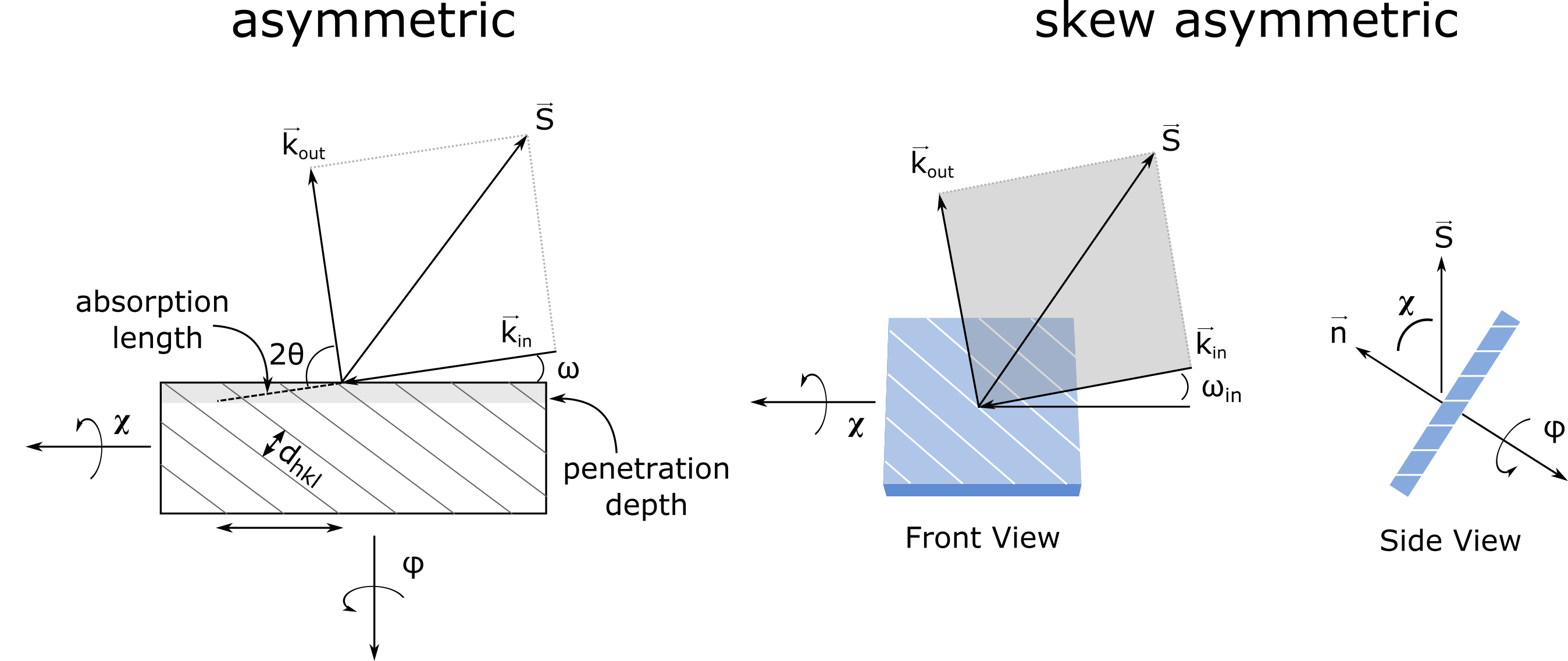
XRD is the standard method for analyzing the structural uniformity of single crystals, however due to the large penetration depth of X-rays in solids compared to thin film thicknesses XRD is unsuitable for the characterization of homoepitaxial thin films–the diffracted intensity is dominated by the substrate. For -Ga2O3, the vertical penetration depth of Cu-K radiation is on the order of 10’s of , while typical thin films are only 100’s of thick, making traditional XRD analysis impossible. Alternative geometries can, however, be considered. Asymmetric geometry refers to an offset in the scattering vector from the surface normal resulting in different incident and exit angles, as shown in Figure 4. Skew geometry refers to a perpendicular tilt of the sample with respect to the incident beam direction, where does not lie within the scattering plane defined by and (represented by the grey plane in Figure 4). In a skew asymmetric geometry, grazing incidence angles may be chosen to geometrically limit the penetration depth to smaller values, effectively attenuating the incident beam within the epilayer[35]. This is schematically depicted in Figure 4, where the incidence angle can be chosen by coincident rotations of the sample along the and axes at a fixed .
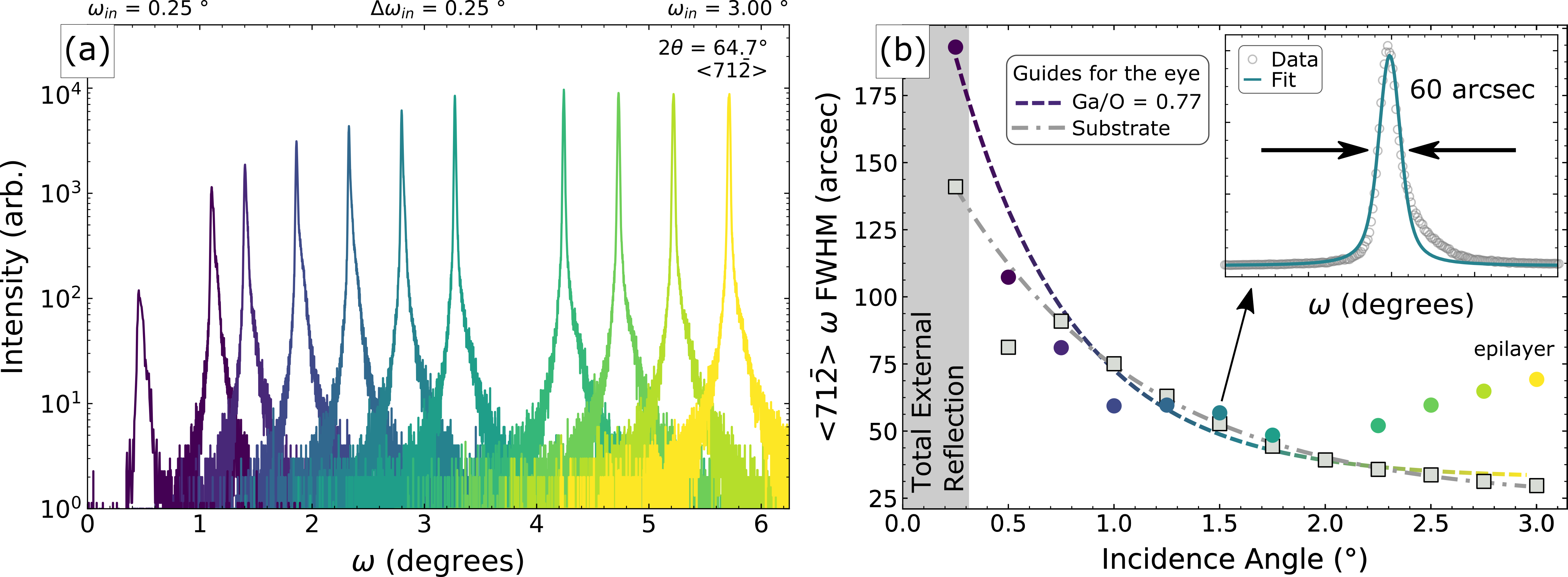
To study structural quality of the epilayers, the normally (010) oriented -Ga2O3 films are analyzed by skew asymmetric XRD at grazing incidence angles along the (71) reflection, chosen for it’s moderate inclination and strong scattering factor. Figure 5 (a) shows rocking curves with incidence angles from for a 185 thick epilayer grown at a Ga/O ratio of 0.77. The goniometer angles used to achieve these measurements are tabulated in the Supplemental Information, Table 2. At low incidence angles, the signal is dominated by the epilayer, but by increasing the incidence angle the penetration depth is rapidly increased, effectively probing the substrate. The resulting full width at half maximum (FWHM), extracted by fitting each rocking curve to a Voigt profile (Figure 5 (b) inset), is plotted in Figure 5 (b). The fit error is at most 3 and is smaller than the size of the plotted data points. This epilayer has a rocking curve FWHM of 193 at a 0.25 incidence angle. It should also be noted that measurements over a wide range of incidence angles, such as that shown in Figure 5, are automated due to long scan times and a requirement to re-optimize at each peak. The data point at 2 degrees incidence angle is omitted because the automation did not successfully optimize the peak and only measured noise. Similar but smaller misalignment issues at higher incidence angles led to a slight decrease in total intensity and a slight increase in FHWM in Figure 5.
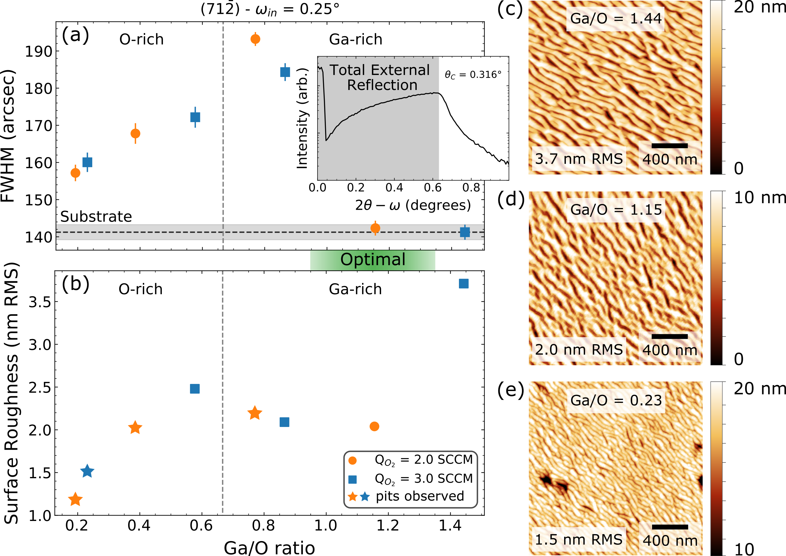
It is important to note that using this method to qualitatively compare samples is only valid if scattering is limited to the epilayer, or if the films are precisely the same thickness. Analysis of substrates without an epilayer show a similar trend of broadening at low incidence angle, with a FWHM of 141 for the lowest measure incidence angle, saturating at approximately 30 for higher incidence angles (Figure 5 (b), grey squares). This broadening is likely due to a large incident X-ray projection on the surface–a geometric effect of extremely low angles. If the length of the beam projected on to the surface is larger than the lateral coherence length of the diffracting crystal (which can be shortened by microstructure, wafer curvature, or surface non-idealities at low angles) then peak broadening will occur[36]. Thus, in order to eliminate the role of thickness variance between different samples the incident angle is chosen to be below the critical angle for total external reflection, measured at 0.316 for -Ga2O3 by X-ray reflectivity (XRR) shown in the inset of Figure 6 (a). In this case evanescent X-rays only penetrate a few in to the film ensuring that all scattering occurs within the epilayer. To ensure instrumental broadening is not dominating the measured signal at these extreme angles, a (100) oriented Si wafer was measured at the (111) reflection using a grazing-incidence skew-asymmetric geometry with an incidence angle of 0.25 ( = 53). The FWHM of (111) Si using the same optics and similar geometry was measured at 18, indicating that instrumental broadening is not a factor in these measurements.
3.3 Structure and morphology
Figure 6 (a) shows the FWHM as a function of Ga/O ratio for for two oxygen flow conditions, based on skew asymmetric rocking curves performed along the (71) reflection fit to a Voigt profile. The Ga/O ratio was determined using the knee in the growth rate versus Ga flux curve as the stoichiometric Ga flux, shown in Figure 2. These XRD measurements were performed in evanescent mode at a grazing incidence angle of 0.25, below the critical angle for total external reflection, to ensure that the diffraction is sensitive to the epilayer[37]. Based on Figure 6 (a), it appears that the epilayer quality is decreased with increasing Ga/O ratio in O-rich growth regime, and then improved at Ga-rich growth conditions. At the skewed geometry ( = 56 ) the incidence angle is a weak function of . To further rule out the effects of a changing penetration depth across the independent variable range, peak widths were also analyzed by rotating following the method reported by Grigoriev et. al.[37], which produced the same qualitative result. A bare substrate was also analyzed (shown by the horizontal dashed line in Figure 6 (a)), giving a baseline broadened value of 141 at 0.25 incidence angle, indicating that films grown at the highest Ga/O ratios are of equal quality to the substrate.
Surface morphology of the -Ga2O3 films was evaluated by AFM as a function of Ga/O ratio during the growth. Surface roughness as a function of Ga/O ratio for films grown at oxygen flows of 2.0 SCCM and 3.0 SCCM is shown in Figure 6 (b) and representative 2 x 2 AFM images are shown in Figure 6 (c-e). In agreement with previous reports, the surface morphology for films grown 700 consist of step-bunching along terraces which propagate along the 100 direction[29]. In Ga-poor growth conditions, adatom diffusion is limited and incorporation occurs before larger terraces can form. For these thin films, all less than 200 nm thick, this results in a lower surface roughness, however that would not hold true for thicker films grown at the same conditions. Low adatom diffusion over the course of a long growth will inevitably lead to roughened growth surfaces–a trend we have observed by RHEED. Films at low Ga/O ratios were also pitted (Figure 6 (e), as annotated by stars in Figure 6 (b). With increasing Ga/O ratio, the scale of the step-bunching increases significantly leading to larger terraces and higher surface roughness (Figure 6 (c)). In the region around stoichiometric growth (2:3 Ga/O ratio) there is very little deviation in the observed surface roughness. For very Ga-rich films the roughness is larger, likely due to partial etching by volatile gallium sub-oxides reported in literature[38]. Therefore, the best surfaces are achieved at slightly Ga-rich conditions (Figure 6 (d)) to minimize surface roughness while also minimizing broadening observed by XRD, indicated by the green bar in Figure 6 (a-b).
Based on combined XRD structural quality and the AFM morphology results it is concluded that slightly Ga-rich films, with a Ga/O ratio of approximately 1.15, produce the highest quality -Ga2O3 epilayers for the studied growth temperature of 700 . According to XRD alone, the best conditions are Ga-rich (Ga/O 1.2) and according to AFM the best conditions are Ga-poor (Ga/O 0.4) followed by slightly Ga-rich (Ga/0 = 0.8 - 1.2); however as noted above this roughness trend may not be true for thicker films. The conclusion about the optimal Ga/O 1.15 growth conditions would not be possible to achieve by either of these techniques alone, highlighting the importance of comprehensive characterization of homoepitaxial layers.
3.4 Electrical characterization
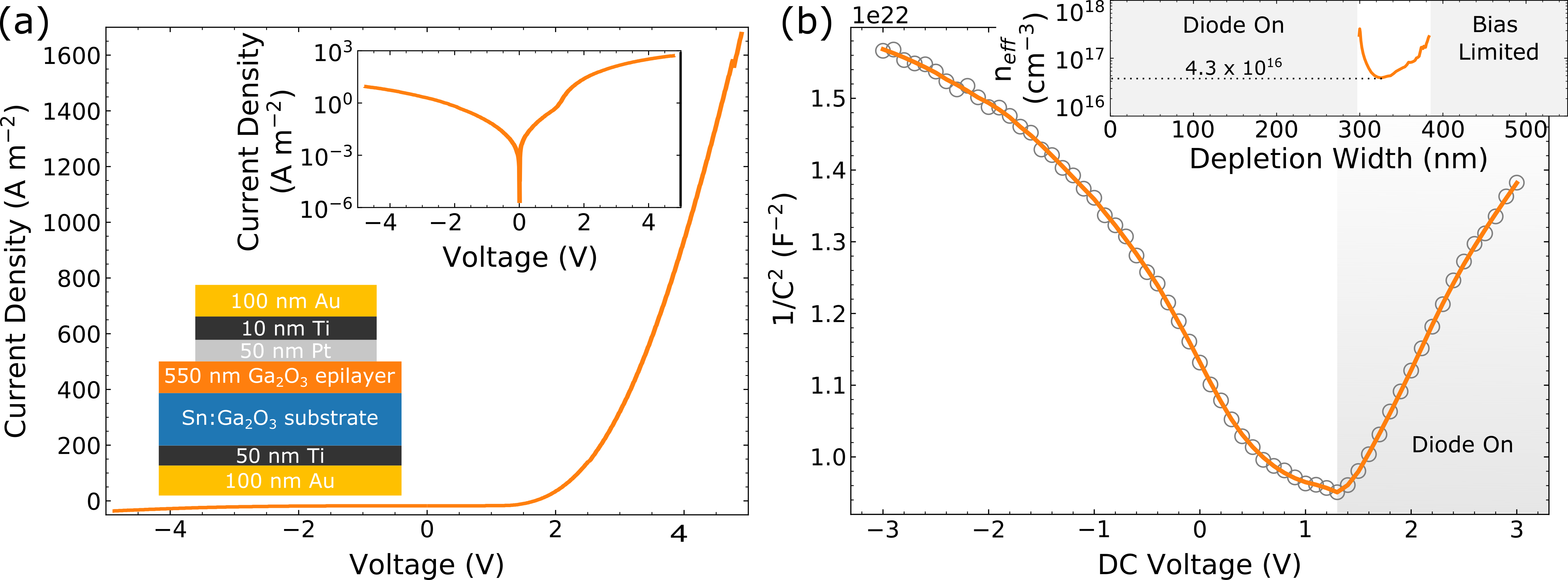
To further study the quality of the homoepitaxially grown -Ga2O3, vertical Schottky barrier diodes based on thicker epilayers (550 nm) grown with a Ga/O ratio of 0.3 were fabricated and electrically characterized. As shown in Figure 7 (a), the fabricated diodes showed current rectification, confirming the formation of Schottky and Ohmic contacts. Fitting to the linear portion of the J-V curve, the turn-on voltage is around = 1.4 , and the on-state resistance is around 230 . The shape of the J-V curve is non-ideal, and the on/off ratio at 2 is quite low, around . More ideal diode behavior and larger on/off ratios were obtained for thinner samples grown at higher Ga/O ratios, consistent with conclusions from combined XRD and AFM analysis. These results indicate that further optimization of the device fabrication process is needed to improve device characteristics, however these non-ideal Schottky barrier diodes were used for capacitance-voltage measurements due to the thicker epilayers.
Capacitance-voltage data for the Schottky barrier diode shown in Figure 7 (a) was subject to Mott-Schottky analysis, as shown in Figure 7 (b). From this data, a doping density was calculated assuming a relative dielectric constant = 11[39], with the results shown in the inset of Figure 7 (b). The effective n-type carrier concentration in the homoepitaxial layer at 320 depth from the surface was determined to be approximately , which is significantly lower than for the Sn-doped substrate, ND - NA = - . The depletion width was probed from approximately , limited on the low side by diode turn-on and on the high side by the applied negative bias. The up-turn in the measured carrier concentration below 320 is due to the positive (but below turn-on) applied DC bias accumulating carriers. These results further confirm the high quality of the homoepitaxial -Ga2O3 layers reported in this study.
4 Summary and Conclusions
In conclusion, we have grown and characterized homoepitaxial -Ga2O3 thin films, focusing on the structural and morphological characteristics of epilayers grown at different Ga/O flux ratios. All defect concentrations are below the SIMS sensitivity limit, with exception of In accumulation at substrate-epilayer interface which is due to the sample mounting scheme. Skew asymmetric XRD at grazing incidence was investigated as a method to characterize the structural quality of homoepitaxial layers, demonstrating the effect of incidence angle on measured film quality as determined by rocking curve analysis. Using grazing incidence angles to selectively analyze epilayer structural quality by operating below the critical angle for total external reflection, we have shown that film quality is improved at Ga-rich growth conditions to the point where the epilayer is of equal structural quality to the substrate. Complementary AFM characterization of the surface reveals increased roughness and step-bunching at increased Ga/O ratios, with films ranging from RMS. Informed by the combination of AFM and skew asymmetric XRD results, it is determined that optimal growth conditions occur at Ga/O ratios of approximately 1.15, when growing at 700 using MBE, however further optimization is needed fine-tune the optimal ratio. Finally, fabricated Schottky barrier diodes characterized by C-V measurements reveal an unintentional doping density of approximately - in the epilayer, consistent with SIMS depth profiles showing no impurities above the noise level. These results show that it is important to use several complementary measurement techniques to characterize the quality of the -Ga2O3 homoepitaxial layers for power electronic applications.
References
References
- [1] Higashiwaki M 2019 MBE Growth and Device Applications of Ga2O3 Molecular Beam Epitaxy: Materials and Applications for Electronics and Optoelectronics (John Wiley & Sons, Ltd) chap 25, pp 411–422 ISBN 9781119354987 URL https://onlinelibrary.wiley.com/doi/abs/10.1002/9781119354987.ch25
- [2] Tsao J Y, Chowdhury S, Hollis M A, Jena D, Johnson N M, Jones K A, Kaplar R J, Rajan S, Walle C G V d, Bellotti E, Chua C L, Collazo R, Coltrin M E, Cooper J A, Evans K R, Graham S, Grotjohn T A, Heller E R, Higashiwaki M, Islam M S, Juodawlkis P W, Khan M A, Koehler A D, Leach J H, Mishra U K, Nemanich R J, Pilawa‐Podgurski R C N, Shealy J B, Sitar Z, Tadjer M J, Witulski A F, Wraback M and Simmons J A 2018 Advanced Electronic Materials 4 1600501 ISSN 2199-160X URL https://onlinelibrary.wiley.com/doi/abs/10.1002/aelm.201600501
- [3] Peelaers H and Walle C G V d 2015 physica status solidi (b) 252 828–832 ISSN 1521-3951 URL https://onlinelibrary.wiley.com/doi/abs/10.1002/pssb.201451551
- [4] Orita M, Ohta H, Hirano M and Hosono H 2000 Applied Physics Letters 77 4166–4168 ISSN 0003-6951 URL https://aip.scitation.org/doi/abs/10.1063/1.1330559
- [5] Ahmadi E, Koksaldi O S, Kaun S W, Oshima Y, Short D B, Mishra U K and Speck J S 2017 Applied Physics Express 10 041102 ISSN 1882-0786 URL http://iopscience.iop.org/article/10.7567/APEX.10.041102/meta
- [6] Krishnamoorthy S, Xia Z, Joishi C, Zhang Y, McGlone J, Johnson J, Brenner M, Arehart A R, Hwang J, Lodha S and Rajan S 2017 Appl. Phys. Lett. 5
- [7] Sasaki K, Higashiwaki M, Kuramata A, Masui T and Yamakoshi S 2013 Journal of Crystal Growth 378 591–595 ISSN 0022-0248 URL http://www.sciencedirect.com/science/article/pii/S0022024813001280
- [8] Reese S B, Remo T, Green J and Zakutayev A 2019 Joule 3 903–907 ISSN 2542-4351 URL http://www.sciencedirect.com/science/article/pii/S2542435119300406
- [9] Galazka Z, Uecker R, Irmscher K, Albrecht M, Klimm D, Pietsch M, Brützam M, Bertram R, Ganschow S and Fornari R 2010 Crystal Research and Technology 45 1229–1236 ISSN 1521-4079 URL https://onlinelibrary.wiley.com/doi/abs/10.1002/crat.201000341
- [10] Aida H, Nishiguchi K, Takeda H, Aota N, Sunakawa K and Yaguchi Y 2008 Japanese Journal of Applied Physics 47 8506 ISSN 1347-4065 URL https://iopscience.iop.org/article/10.1143/JJAP.47.8506/meta
- [11] Wenckstern H v 2017 Advanced Electronic Materials 3 1600350 ISSN 2199-160X URL https://www.onlinelibrary.wiley.com/doi/abs/10.1002/aelm.201600350
- [12] Qin Y, Long S, Dong H, He Q, Jian G, Zhang Y, Hou X, Tan P, Zhang Z, Lv H, Liu Q and Liu M 2019 Chinese Physics B 28 018501 ISSN 1674-1056 URL https://iopscience.iop.org/article/10.1088/1674-1056/28/1/018501
- [13] Chabak K D, Leedy K D, Green A J, Mou S, Neal A T, Asel T, Heller E R, Hendricks N S, Liddy K, Crespo A, Miller N C, Lindquist M T, Moser N A, Fitch R C, Walker D E, Dorsey D L and Jessen G H 2019 Semiconductor Science and Technology 35 013002 ISSN 0268-1242 URL https://iopscience.iop.org/article/10.1088/1361-6641/ab55fe
- [14] Higashiwaki M, Kuramata A, Murakami H and Kumagai Y 2017 Journal of Physics D: Applied Physics 50 333002 ISSN 0022-3727 URL https://iopscience.iop.org/article/10.1088/1361-6463/aa7aff
- [15] Afzal A 2019 Journal of Materiomics 5 542–557 ISSN 2352-8478 URL http://www.sciencedirect.com/science/article/pii/S235284781930067X
- [16] Pearton S J, Yang J, Cary P H, Ren F, Kim J, Tadjer M J and Mastro M A 2018 Applied Physics Reviews 5 011301 URL https://aip.scitation.org/doi/10.1063/1.5006941
- [17] Ahmadi E, Koksaldi O S, Zheng X, Mates T, Oshima Y, Mishra U K and Speck J S 2017 Applied Physics Express 10 071101 ISSN 1882-0778, 1882-0786 URL https://iopscience.iop.org/article/10.7567/APEX.10.071101
- [18] Moser N, McCandless J, Crespo A, Leedy K, Green A, Neal A, Mou S, Ahmadi E, Speck J, Chabak K, Peixoto N and Jessen G 2017 IEEE Electron Device Letters 38 775–778 ISSN 0741-3106 URL https://ieeexplore.ieee.org/document/7911200
- [19] Liu Z, Li P G, Zhi Y S, Wang X L, Chu X L and Tang W H 2019 Chinese Physics B 28 017105 ISSN 1674-1056 URL https://iopscience.iop.org/article/10.1088/1674-1056/28/1/017105
- [20] Li W, Nomoto K, Hu Z, Jena D and Xing H G 2020 IEEE Electron Device Letters 41 107–110 ISSN 1558-0563 URL https://ieeexplore.ieee.org/document/8901439
- [21] Allen N, Xiao M, Yan X, Sasaki K, Tadjer M J, Ma J, Zhang R, Wang H and Zhang Y 2019 IEEE Electron Device Letters 40 1399–1402 ISSN 1558-0563 URL https://ieeexplore.ieee.org/document/8779668
- [22] Wong M H, Goto K, Murakami H, Kumagai Y and Higashiwaki M 2019 IEEE Electron Device Letters 40 431–434 ISSN 1558-0563 URL https://ieeexplore.ieee.org/document/8556005
- [23] Hu Z, Nomoto K, Li W, Tanen N, Sasaki K, Kuramata A, Nakamura T, Jena D and Xing H G 2018 IEEE Electron Device Letters 39 869–872 ISSN 1558-0563 URL https://ieeexplore.ieee.org/document/8347056
- [24] Slomski M, Blumenschein N, Paskov P P, Muth J F and Paskova T 2017 Journal of Applied Physics 121 235104 ISSN 0021-8979 URL https://aip.scitation.org/doi/full/10.1063/1.4986478
- [25] Cheng Z, Yates L, Shi J, Tadjer M J, Hobart K D and Graham S 2019 APL Materials 7 031118 URL https://aip.scitation.org/doi/full/10.1063/1.5089559
- [26] Kyrtsos A, Matsubara M and Bellotti E 2018 Applied Physics Letters 112 032108 ISSN 0003-6951 URL https://aip.scitation.org/doi/10.1063/1.5009423
- [27] Peelaers H, Lyons J L, Varley J B and Van de Walle C G 2019 APL Materials 7 022519 URL https://aip.scitation.org/doi/10.1063/1.5063807
- [28] Okumura H, Kita M, Sasaki K, Kuramata A, Higashiwaki M and Speck J S 2014 Applied Physics Express 7 095501 ISSN 1882-0786 URL http://iopscience.iop.org/article/10.7567/APEX.7.095501/meta
- [29] Sasaki K 2014 Journal of Crystal Growth 4 URL https://iopscience.iop.org/article/10.7567/APEX.7.095501/meta
- [30] Oshima T, Arai N, Suzuki N, Ohira S and Fujita S 2008 Thin Solid Films 516 5768–5771 ISSN 0040-6090 URL http://www.sciencedirect.com/science/article/pii/S004060900701721X
- [31] Lee S d, Kaneko K and Fujita S 2016 Japanese Journal of Applied Physics 55 1202B8 ISSN 1347-4065 URL https://iopscience.iop.org/article/10.7567/JJAP.55.1202B8/meta
- [32] Mahadik N A, Tadjer M J, Bonanno P L, Hobart K D, Stahlbush R E, Anderson T J and Kuramata A 2019 APL Materials 7 022513 URL https://doi.org/10.1063/1.5051633
- [33] LeBeau J M, Engel-Herbert R, Jalan B, Cagnon J, Moetakef P, Stemmer S and Stephenson G B 2009 Applied Physics Letters 95 142905 ISSN 0003-6951 URL https://aip.scitation.org/doi/10.1063/1.3243696
- [34] Stull D R 1947 Industrial & Engineering Chemistry 39 540–550 ISSN 0019-7866 URL https://pubs.acs.org/doi/abs/10.1021/ie50448a023
- [35] Swiatek Z, Fodchuk I and Zaplitnyy R 2017 Journal of Applied Crystallography 50 727–733 ISSN 0021-8898 URL https://www.ncbi.nlm.nih.gov/pmc/articles/PMC5458592/
- [36] Pietsch U, Holy V and Baumbach T 2004 High-Resolution X-Ray Scattering: From Thin Films to Lateral Nanostructures 2nd ed Advanced Texts in Physics (New York: Springer-Verlag) ISBN 978-0-387-40092-1 URL https://www.springer.com/gp/book/9780387400921
- [37] Grigoriev D, Lazarev S, Schroth P, Minkevich A, Köhl M, Slobodskyy T, Helfrich M, Schaadt D, Aschenbrenner T, Hommel D and Baumbach T 2016 Journal of Applied Crystallography 49 URL http://scripts.iucr.org/cgi-bin/paper?S1600576716006385
- [38] Vogt P and Bierwagen O 2015 Applied Physics Letters 106 081910 ISSN 0003-6951 URL https://aip.scitation.org/doi/10.1063/1.4913447
- [39] Fiedler A, Schewski R, Galazka Z and Irmscher K 2019 ECS Journal of Solid State Science and Technology 8(7) Q3083–Q3085 URL https://iopscience.iop.org/article/10.1149/2.0201907jss