Superconductivity without insulating states in twisted bilayer graphene stabilized by monolayer WSe2
Abstract
Magic-angle twisted bilayer graphene (TBG), with rotational misalignment close to 1.1°, features isolated flat electronic bands that host a rich phase diagram of correlated insulating, superconducting, ferromagnetic, and topological phases[1, 2, 3, 4, 5, 6]. The origins of the correlated insulators and superconductivity, and the interplay between them, are particularly elusive due to the sensitivity of these correlated states to microscopic details. Both states have been previously observed only for angles within 0.1° from the magic-angle value and occur in adjacent or overlapping electron density ranges; nevertheless, it is still unclear how the two states are related. Beyond the twist angle and strain, the dependence of the TBG phase diagram on the alignment[4, 6] and thickness of insulating hexagonal boron nitride (hBN)[7, 8] used to encapsulate the graphene sheets indicates the importance of the microscopic dielectric environment. Here we show that adding an insulating tungsten-diselenide (WSe2) monolayer between hBN and TBG stabilizes superconductivity at twist angles much smaller than the established magic-angle value. For the smallest angle of = 0.79°, we still observe clear superconducting signatures, despite the complete absence of the correlated insulating states and vanishing gaps between the dispersive and flat bands. These observations demonstrate that, even though electron correlations may be important, superconductivity in TBG can exist even when TBG exhibits metallic behaviour across the whole range of electron density. Finite-magnetic-field measurements further reveal breaking of the four-fold spin-valley symmetry in the system, consistent with large spin-orbit coupling induced in TBG via proximity to WSe2. The survival of superconductivity in the presence of spin-orbit coupling imposes additional constraints on the likely pairing channels. Our results highlight the importance of symmetry breaking effects in stabilizing electronic states in TBG and open new avenues for engineering quantum phases in moiré systems.
T. J. Watson Laboratory of Applied Physics, California Institute of Technology, 1200 East California Boulevard, Pasadena, California 91125, USA
Institute for Quantum Information and Matter, California Institute of Technology, Pasadena, California 91125, USA
Department of Physics, California Institute of Technology, Pasadena, California 91125, USA
Walter Burke Institute for Theoretical Physics, California Institute of Technology, Pasadena, California 91125, USA
Department of Physics, University of Washington, Seattle, Washington 98195, USA
Department of Materials Science and Engineering, University of Washington, Seattle, WA 98195, USA
National Institute for Materials Science, Namiki 1-1, Tsukuba, Ibaraki 305 0044, Japan
These authors contributed equally to this work
Correspondence: s.nadj-perge@caltech.edu
Strongly correlated electron systems often exhibit a variety of quantum phases with similar ground-state energies, separated by phase boundaries that depend sensitively on microscopic details. Twisted bilayer graphene, with twist angle close to the magic angle M 1.1°, has recently emerged as a highly tunable platform with an exceptionally rich phase diagram[1, 2] hosting correlated insulating states, superconductivity, and ferromagnetism[3, 4, 5, 6]. Strong correlations in TBG originate from the non-dispersive (flat) bands that are created by the hybridization of the graphene sheets[9] and are isolated from the rest of the energy spectrum by an energy gap 30 meV[10, 11]. Previous transport experiments on magic-angle TBG found that the correlated insulators are often accompanied by superconductivity in a narrow range 0.1° around M[1, 3, 8, 7, 12], with signatures of these states observed down to 0.93°[13]. Close to M, the correlated insulators develop at electron densities that correspond to an integer number of electrons per moiré unit and are surrounded by intermittent pockets of superconductivity[5]; both phases appear most frequently around = 2[2, 3]. Away from M, however, both phases are suppressed as the effects of electron-electron interactions quickly diminish due to a rapid increase of the flat-band bandwidth and corresponding dominance of kinetic energy[9, 1]. In addition to the TBG twist angle, the physics of the correlated phases is also affected by the hBN employed as a high-quality dielectric. In particular, since hBN and graphene exhibit similar crystal lattices, the relative alignment between the hBN and TBG is critical. For example, a ferromagnetic state near = +3 was observed in devices where hBN aligns with TBG[4, 6]. However, in such devices the band structure of the flat bands is strongly altered[6], and superconductivity—typically observed when hBN and TBG are misaligned—is absent. Recent work using a very thin hBN layer separating a back gate from TBG additionally suggests that electrostatic screening plays a prominent role in the appearance of insulating and superconducting states[7]. These experiments exemplify the effects of hBN layers on the phase diagram in hBN-TBG-hBN structures and highlight the importance of understanding how microscopic details of the dielectric environment alter the properties of correlated phases.
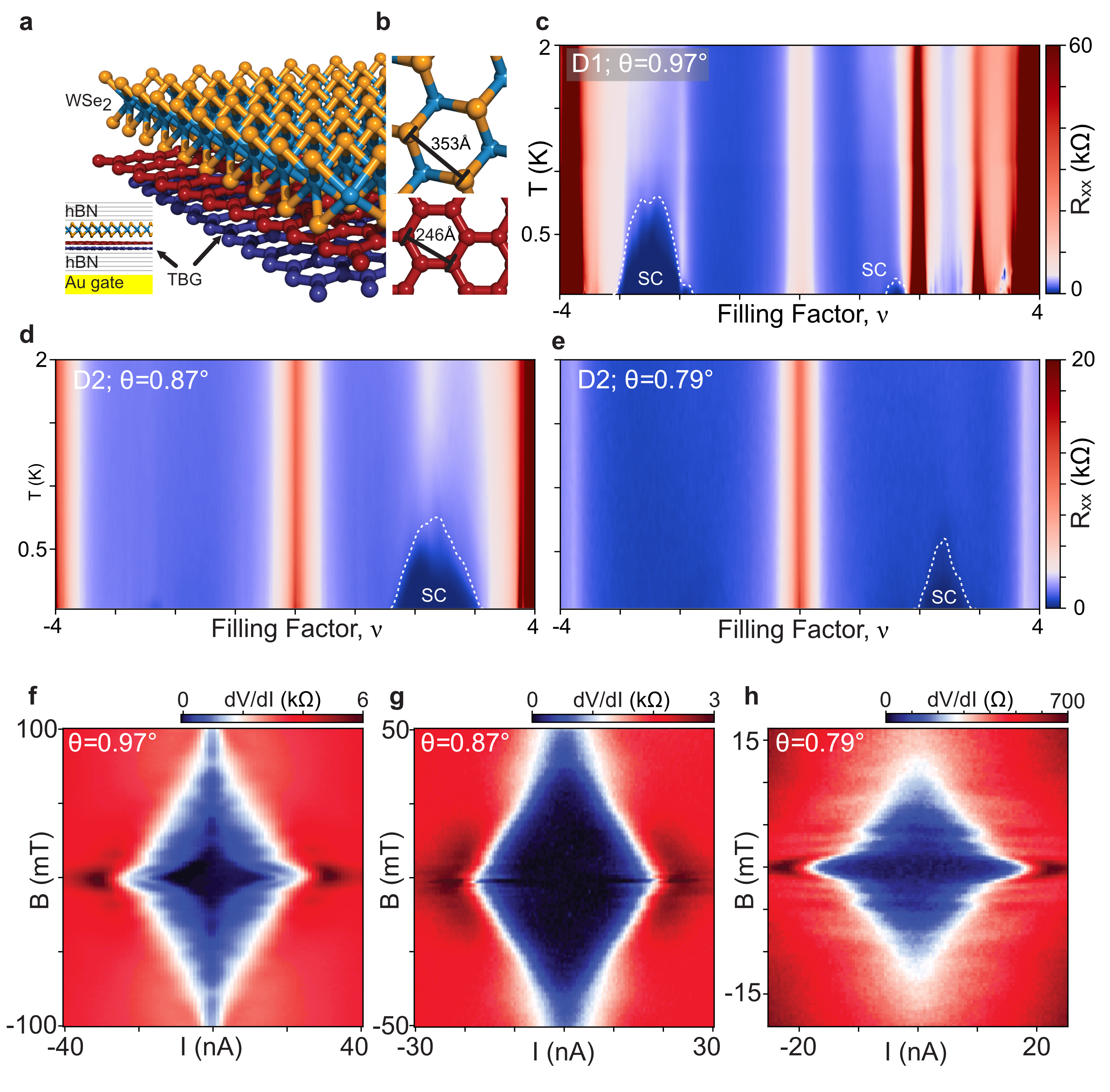
Here, instead of the usual hBN-TBG-hBN structures, we investigate devices made from hBN-TBG-WSe2-hBN van der Waals stacks in which a monolayer of WSe2 resides between the top hBN and TBG (Fig. 1a). Our stacks are assembled using a modified ‘tear and stack’ technique where the ‘tearing’ and ‘stacking’ of TBG is facilitated by monolayer WSe2; see Methods and Extended Data Fig. 1 for fabrication details. Like hBN, flakes of transition metal dichalcogenides, such as WSe2, can be used as a high-quality insulating dielectric for graphene-based devices[14]; however, the two van der Waals dielectrics differ in several ways that may alter the TBG band structure. First, unlike hBN, the WSe2 and graphene lattice constants differ significantly (0.353 nm for WSe2 and 0.246 nm for graphene, Fig. 1b). This mismatch implies that the moiré pattern formed between TBG and WSe2 has a maximum lattice constant 1 nm, in other words, much smaller than that formed in small-angle TBG ( 10 nm). Second, it is well-established that WSe2 can induce a spin-orbit interaction (SOI) in graphene via van der Waals proximity[15, 16]. And finally, due to hybridization effects, WSe2 may also change both the Fermi velocity of the proximitized graphene sheet and the system’s phonon spectrum. We chose to use monolayer WSe2 in particular because of its large band gap[17] that allows applying a large range of gate voltages. It has also been suggested previously that a monolayer induces larger spin-orbit coupling in graphene compared to a few-layer WSe2[18].
We have studied three TBG-WSe2 devices and show results for two of them in the main text (see Extended Data Fig. 4 for data from an additional device). Surprisingly, we find robust superconductivity in all studied TBG-WSe2 structures, even for twist angles far outside of the previously established range. Fig. 1c-e shows the temperature dependence of resistance over three TBG regions corresponding to angles = 0.97°, = 0.87° and = 0.79°; in all cases superconducting transitions are clearly visible. Aside from the drop in Rxx to zero, we also observe well-resolved Fraunhofer-like patterns for all three angles (Figs. 1f-1h), qualitatively similar to the typical hBN-TBG-hBN devices[2, 5, 3]. The small periodic modulations of the critical current in magnetic field have been previously attributed to the presence of Josephson junctions in the system, independently corroborating the presence of superconducting correlations. In our devices, we typically see periods of 1.5-3 mT that, if interpreted as the effective junction area 0.67–1.33 µm2, are consistent with the device geometry.
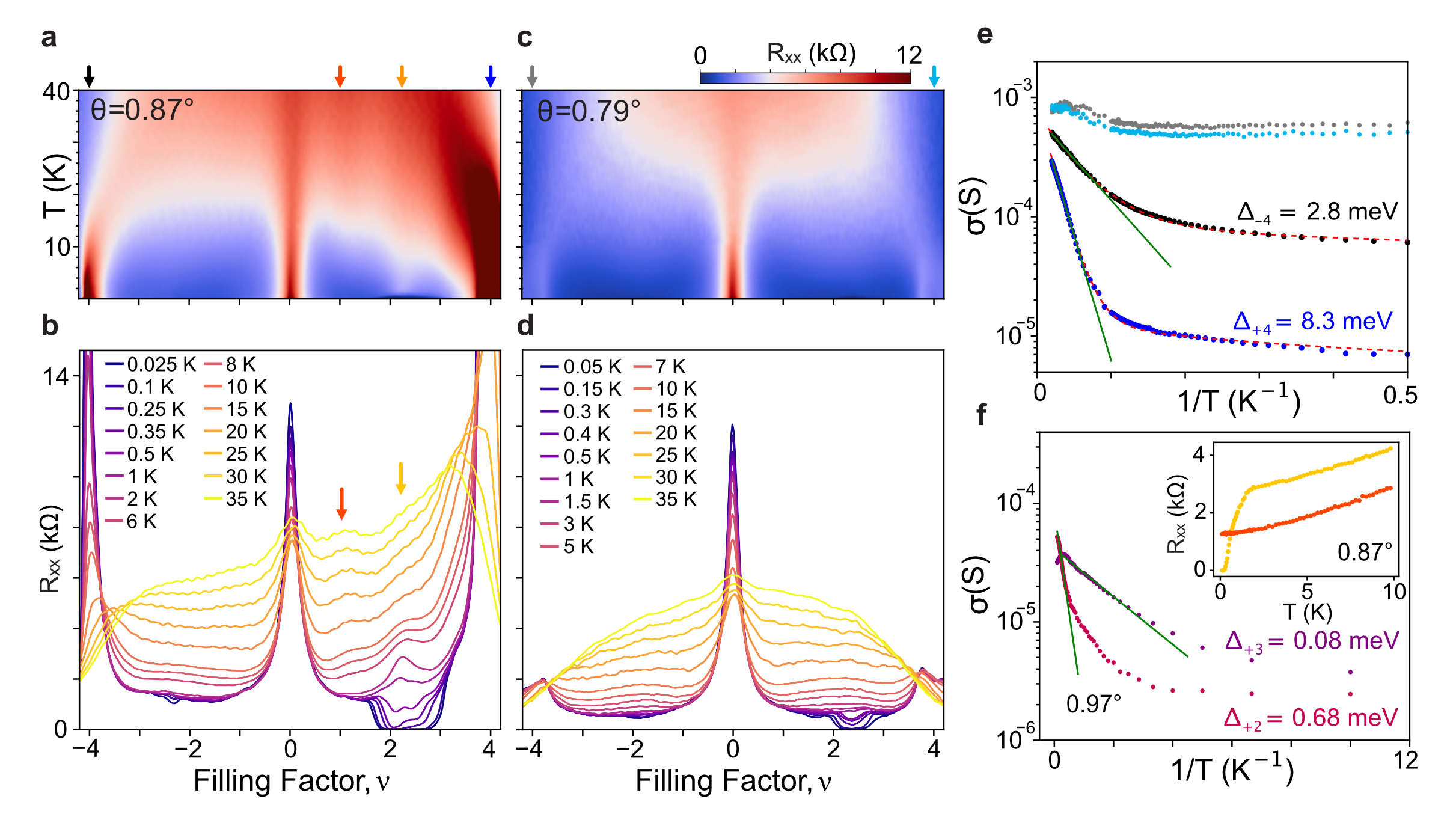
For the largest angle = 0.97°, a superconducting pocket emerges on the hole side near = –2 with a maximal transition temperature Tc 0.8 K. To our knowledge, this already is the smallest angle for which superconductivity has been observed for hole doping. Careful inspection reveals another weak superconductivity pocket close to = +2 (the behavior at low fields is displayed in Extended Data Fig. 6). However, despite the small twist angle—falling outside the M 0.1° range—the observed phase diagram resembles that of regular high-quality magic-angle hBN-TBG-hBN structures[2, 5]. For this angle, correlated insulating states are also observed for filling factors = +2, +3 with activation gaps of = 0.68 meV and = 0.08 meV, whereas at other filling factors correlated states are less developed and do not show insulting behavior (see Fig. 2f and Extended Data Fig. 3).
Although superconductivity persists for all three angles, the correlated insulators are quickly suppressed as the twist angle is reduced. This suppression is not surprising, as for angles below M, the bandwidth increases rapidly and, moreover, the characteristic correlation energy scale also diminishes due to an increase in the moiré periodicity = ( = 0.246 nm denotes the graphene lattice constant)[9, 1, 19, 10, 20, 21]. For the lower angle of = 0.87° correlated-insulating behavior is heavily suppressed at all filling factors. In Fig. 1d a peak in longitudinal resistance versus density is visible only around = +2 above the superconducting transition ( = 600–800 mK). Data for a larger temperature range (Fig. 2a-b) shows that the resistance peak near = +2 survives up to = 30 K, and also reveals a new peak near = +1 in the temperature range 10-35 K. These observations suggest that electron correlations remain strong, though the corresponding states appear to be metallic as the overall resistance increases with temperature. For this angle, we measure activation gaps at full filling (i.e., at = ) of = 8.3 meV and = 2.8 meV (Fig. 2e) —far smaller than the gaps around , in line with previous results that report a disappearance of the band gap separating dispersive and flat bands at around = 0.8°[22, 11].
At the smallest angle, = 0.79°, along with the lack of insulating states at any partial filling, the resistance at full filling is even more reduced (Fig. 2c-d). The relatively low resistances <2 k\textOmega measured at full filling—which are less than of the resistance at the charge neutrality point (CNP)—suggest a semi-metallic band structure around full filling, consistent with theoretical expectations for TBG at = 0.79°[22] and the resistivity of a dilute 2D electron gas[23]. We emphasize, however, that despite the absence of both full-filling band gaps and correlated insulators, the superconducting low-resistance pocket near is clearly resolved (Figs. 1e and 1h).
Both the disappearance of the correlated insulators and the vanishing gap between flat and dispersive bands for low angles suggest that the additional WSe2 monolayer does not significantly change the magic angle. Since superconductivity survives to much lower angles compared to correlated insulating states, the two phenomena appear to have different origins[7, 8]. Note also that the close proximity of the dispersive bands does not seem to have a major impact on the superconducting phase. While these findings are not consistent with a scenario wherein superconductivity descends from a Mott-like insulating state as in high-Tc superconductors[24], we do emphasize that electron correlations may still prove essential for the development of superconductivity. For instance, even for the smallest angle of = 0.79°, the superconducting pocket is seemingly pinned to the vicinity of = 2. Additionally, as shown in Fig. 2, at higher temperatures residual Rxx peaks can still appear at certain integer filling factors despite the absence of gapped correlated insulating states. It is thus hard to rule out the possibility that superconductivity arises from correlated states of metallic nature that may be present at smaller angles and near integer values of in analogy to other exotic superconducting systems[25, 26, 27].
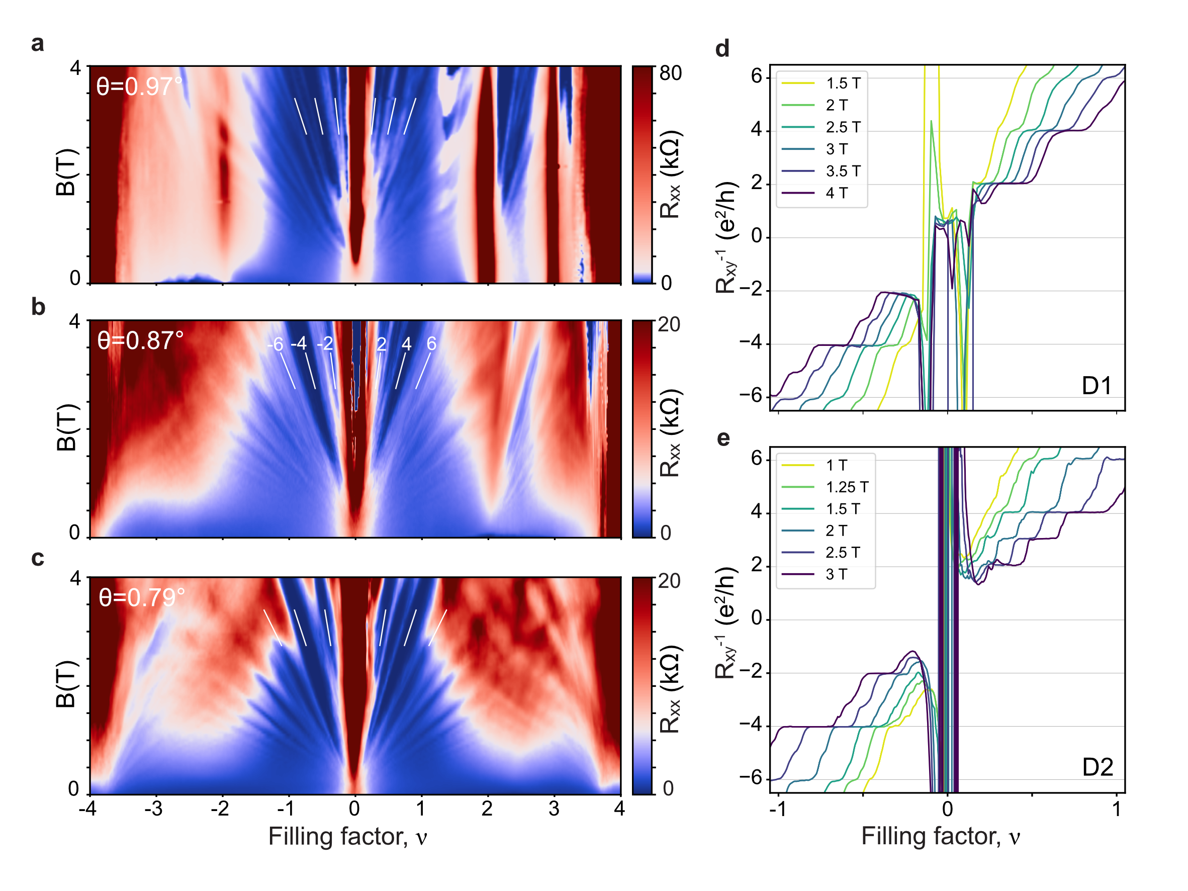
Measurements in finite magnetic field reveal further insights into the physics of TBG-WSe2 structures (Fig. 3). Surprisingly, for all three angles we find that even at modest magnetic fields, above = 1 T, gaps between Landau levels are well-resolved, showing a fan diagram that diverges from the CNP. The slopes of the dominant sequence of Rxx minima correspond to even-integer Landau level fillings 2, 4, , etc.—indicating broken four-fold (spin-valley flavor) symmetry. By contrast, the majority of previous transport experiments[2, 3] near the magic angle report a Landau-fan sequence 4, 8, 12 at the CNP, with broken-symmetry states being only occasionally observed at the lowest Landau level (corresponding to the 2 sequence)[4, 5, 28]. In addition to Rxx minima corresponding to the gaps between Landau levels, we also measured quantized Hall conductance plateaus, further corroborating the two-fold symmetry and indicating the low disorder in the measured TBG areas. Note also that for the smallest angle ( = 0.79° ) we do not observe obvious signatures of correlated insulating states near = 2 up to = 4 T.
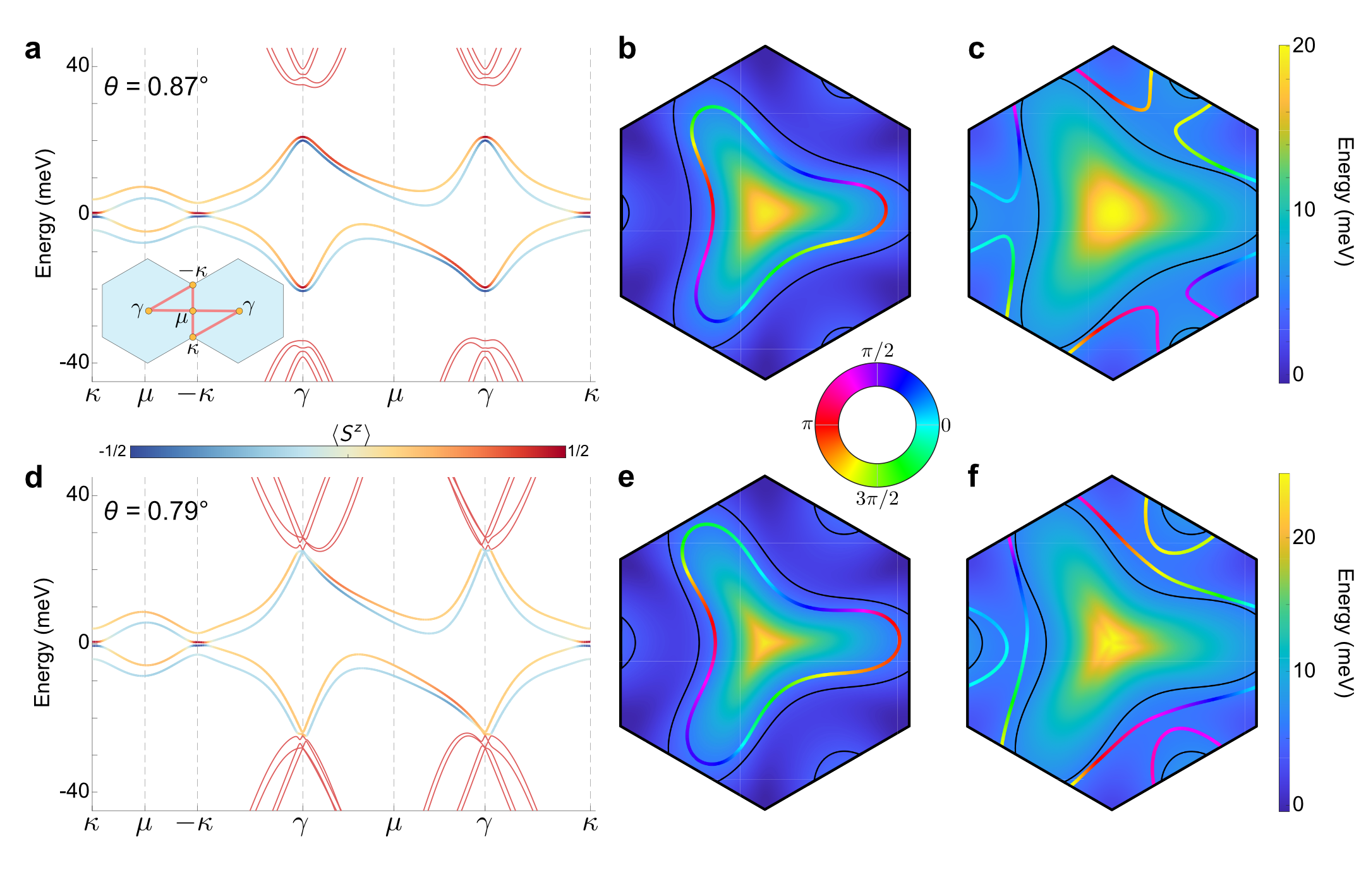
The observed two-fold degeneracy is consistent with a scenario in which the TBG band structure is modified by the spin-orbit interaction (SOI) inherited from the WSe2 monolayer (Fig. 4). Previous works established that WSe2 can induce large SOI of both Ising and Rashba type into monolayer and bilayer graphene[15, 16], and it is therefore reasonable to assume that the SOI is similarly generated in the upper (proximitized) layer of TBG in our devices. Continuum-model calculations taking into account this effect show that the SOI lifts the degeneracy of both flat and dispersive bands, thereby breaking four-fold spin-valley symmetry. In a finite magnetic field, the resulting Landau levels then descend from Kramer’s states that are only two-fold degenerate. Odd steps—which are not generated by the SOI—are occasionally observed for low angles. We attribute these steps to additional symmetry breaking, possibly due to correlation effects originating either from flat-band physics or simply a magnetic-field-induced effect at low electronic densities.
Induced SOI can additionally constrain the nature of the TBG phase diagram. In particular, the SOI acts as an explicit symmetry-breaking field that further promotes instabilities favoring compatible symmetry-breaking patterns while suppressing those that do not. The relative robustness of the = 2 correlated insulator in our = 0.97° device suggests that interactions favor re-populating bands[29, 30] in a manner that also satisfies the spin-orbit energy. Furthermore, the survival of superconductivity with SOI constrains the plausible pairing channels—particularly given the dramatic spin-orbit-induced Fermi-surface deformations that occur at = +2 (Fig. 4). Superconductivity in our low-twist-angle devices, for instance, is consistent with Cooper pairing of time-reversed partners that remain resonant with SOI. Thus the stability of candidate insulating and superconducting phases to the SOI provides a nontrivial constraint for theory[31, 32, 33, 34, 35]. The integration of monolayer WSe2 demonstrates the impact of the van der Waals environment and proximity effects on the rich phase diagram of TBG. In a broader context, this approach opens the future prospect of controlling the range of novel correlated phases available in TBG and similar structures by carefully engineering the surrounding layers, and it highlights a key tool for disentangling the mechanisms driving the different correlated states.
References:
References
- [1] Cao, Y. et al. Correlated insulator behaviour at half-filling in magic-angle graphene superlattices. Nature 556, 80–84 (2018).
- [2] Cao, Y. et al. Unconventional superconductivity in magic-angle graphene superlattices. Nature 556, 43–50 (2018).
- [3] Yankowitz, M. et al. Tuning superconductivity in twisted bilayer graphene. Science 363, 1059–1064 (2019).
- [4] Sharpe, A. L. et al. Emergent ferromagnetism near three-quarters filling in twisted bilayer graphene. Science 365, 605–608 (2019).
- [5] Lu, X. et al. Superconductors, orbital magnets and correlated states in magic-angle bilayer graphene. Nature 574, 653–657 (2019).
- [6] Serlin, M. et al. Intrinsic quantized anomalous Hall effect in a moiré heterostructure. Science (2019).
- [7] Stepanov, P. et al. The interplay of insulating and superconducting orders in magic-angle graphene bilayers. arXiv:1911.09198 [cond-mat] (2019). 1911.09198.
- [8] Saito, Y., Ge, J., Watanabe, K., Taniguchi, T. & Young, A. F. Decoupling superconductivity and correlated insulators in twisted bilayer graphene. arXiv:1911.13302 [cond-mat] (2019). 1911.13302.
- [9] Bistritzer, R. & MacDonald, A. H. Moiré bands in twisted double-layer graphene. Proceedings of the National Academy of Sciences 108, 12233–12237 (2011).
- [10] Choi, Y. et al. Electronic correlations in twisted bilayer graphene near the magic angle. Nature Physics 15, 1174–1180 (2019).
- [11] Polshyn, H. et al. Large linear-in-temperature resistivity in twisted bilayer graphene. Nature Physics 15, 1011–1016 (2019).
- [12] Cao, Y. et al. Strange metal in magic-angle graphene with near Planckian dissipation. arXiv:1901.03710 [cond-mat] (2019). 1901.03710.
- [13] Codecido, E. et al. Correlated insulating and superconducting states in twisted bilayer graphene below the magic angle. Science Advances 5, eaaw9770 (2019).
- [14] Kretinin, A. V. et al. Electronic Properties of Graphene Encapsulated with Different Two-Dimensional Atomic Crystals. Nano Letters 14, 3270–3276 (2014).
- [15] Island, J. O. et al. Spin–orbit-driven band inversion in bilayer graphene by the van der Waals proximity effect. Nature 571, 85–89 (2019).
- [16] Wang, D. et al. Quantum Hall Effect Measurement of Spin–Orbit Coupling Strengths in Ultraclean Bilayer Graphene/WSe2 Heterostructures. Nano Letters 19, 7028–7034 (2019).
- [17] Wilson, N. R. et al. Determination of band offsets, hybridization, and exciton binding in 2D semiconductor heterostructures. Science Advances 3, e1601832 (2017).
- [18] Wakamura, T. et al. Spin-orbit interaction induced in graphene by transition metal dichalcogenides. Physical Review B 99, 245402 (2019).
- [19] Kerelsky, A. et al. Maximized electron interactions at the magic angle in twisted bilayer graphene. Nature 572, 95–100 (2019).
- [20] Xie, Y. et al. Spectroscopic signatures of many-body correlations in magic-angle twisted bilayer graphene. Nature 572, 101–105 (2019).
- [21] Jiang, Y. et al. Charge order and broken rotational symmetry in magic-angle twisted bilayer graphene. Nature 573, 91–95 (2019).
- [22] Koshino, M. et al. Maximally Localized Wannier Orbitals and the Extended Hubbard Model for Twisted Bilayer Graphene. Physical Review X 8, 031087 (2018).
- [23] Lilly, M. P. et al. Resistivity of Dilute 2D Electrons in an Undoped GaAs Heterostructure. Physical Review Letters 90, 056806 (2003).
- [24] Lee, P. A., Nagaosa, N. & Wen, X.-G. Doping a Mott insulator: Physics of high-temperature superconductivity. Reviews of Modern Physics 78, 17–85 (2006).
- [25] Stewart, G. R. Heavy-fermion systems. Reviews of Modern Physics 56, 755–787 (1984).
- [26] Ardavan, A. et al. Recent Topics of Organic Superconductors. Journal of the Physical Society of Japan 81, 011004 (2011).
- [27] Stewart, G. R. Superconductivity in iron compounds. Reviews of Modern Physics 83, 1589–1652 (2011).
- [28] Uri, A. et al. Mapping the twist angle and unconventional Landau levels in magic angle graphene. arXiv:1908.04595 [cond-mat] (2019). 1908.04595.
- [29] Zondiner, U. et al. Cascade of Phase Transitions and Dirac Revivals in Magic Angle Graphene. arXiv:1912.06150 [cond-mat] (2019). 1912.06150.
- [30] Wong, D. et al. Cascade of transitions between the correlated electronic states of magic-angle twisted bilayer graphene. arXiv:1912.06145 [cond-mat] (2019). 1912.06145.
- [31] Guinea, F. & Walet, N. R. Electrostatic effects, band distortions, and superconductivity in twisted graphene bilayers. Proceedings of the National Academy of Sciences 115, 13174–13179 (2018).
- [32] You, Y.-Z. & Vishwanath, A. Superconductivity from valley fluctuations and approximate SO(4) symmetry in a weak coupling theory of twisted bilayer graphene. npj Quantum Materials 4, 1–12 (2019).
- [33] Lian, B., Wang, Z. & Bernevig, B. A. Twisted Bilayer Graphene: A Phonon-Driven Superconductor. Physical Review Letters 122, 257002 (2019).
- [34] Kozii, V., Isobe, H., Venderbos, J. W. F. & Fu, L. Nematic superconductivity stabilized by density wave fluctuations: Possible application to twisted bilayer graphene. Physical Review B 99, 144507 (2019).
- [35] Gu, X. et al. Antiferromagnetism and chiral d-wave superconductivity from an effective $t-J-D$ model for twisted bilayer graphene. arXiv:1902.00029 [cond-mat] (2019). 1902.00029.
- [36] Cao, Y. et al. Superlattice-Induced Insulating States and Valley-Protected Orbits in Twisted Bilayer Graphene. Physical Review Letters 117, 116804 (2016).
Acknowledgments: We acknowledge discussions with Hechen Ren, Ding Zhong, Yang Peng, Gil Refael, Felix von Oppen, Jim Eisenstein, and Patrick Lee. The device nanofabrication was performed at the Kavli Nanoscience Institute (KNI) at Caltech. Funding: This work was supported by NSF through program CAREER DMR-1753306 and grant DMR-1723367, Gist-Caltech memorandum of understanding and the Army Research Office under Grant Award W911NF-17-1-0323. Nanofabrication performed by Y.Z. has been supported by DOE-QIS program (DE-SC0019166). J.A. and S.N.-P. also acknowledge the support of IQIM (NSF funded physics frontiers center). A.T. and J.A. are grateful for support from the Walter Burke Institute for Theoretical Physics at Caltech and the Gordon and Betty Moore Foundation’s EPiQS Initiative, Grant GBMF8682. The material synthesis at UW was supported as part of Programmable Quantum Materials, an Energy Frontier Research Center funded by the U.S. Department of Energy (DOE), Office of Science, Basic Energy Sciences (BES), under award DE-SC0019443 and the Gordon and Betty Moore Foundation’s EPiQS Initiative, Grant GBMF6759 to J.-H.C.
Author Contribution: H.A., R.P., Y.Z., and S.N.-P. designed the experiment. H.A. made the TBG-WSe2 devices assisted by Y.Z., H.K. and Y.C. H.A. and R.P., performed the measurements. Y.Z. performed measurements on initial TBG devices. H.A., R.P., and S.N.-P. analyzed the data. A.T. and J.A. developed the continuum model that includes spin-orbit interaction and performed model calculations. Z.L., I.Z.W., X.X., and J.-H.C. provided WSe2 crystals. K.W. and T.T. provided hBN crystals. H.A., R.P., Y.Z., A.T., J.A., and S.N.-P. wrote the manuscript with input from other authors. S.N.-P. supervised the project.
Data availability: The data that support the findings of this study are available from the corresponding authors on reasonable request.


