Thermal conductivity of Bi2Se3 from bulk to thin films: theory and experiment.
Abstract
We calculate the lattice-driven in-plane and out-of-plane thermal conductivities of Bi2Se3 bulk, and of films of different thicknesses, using the Boltzmann equation with phonon scattering times obtained from anharmonic third order density functional perturbation theory. We compare our results for the lattice component of the thermal conductivity with published data for on bulk samples and with our room-temperature thermoreflectance measurements of on films of thickness (L) ranging from 18 nm to 191 nm, where the lattice component has been extracted via the Wiedemann-Franz law. Ab-initio theoretical calculations on bulk samples, including an effective model to account for finite sample thickness and defect scattering, compare favorably both for the bulk case (from literature) and thin films (new measurements). In the low-T limit the theoretical in-plane lattice thermal conductivity of bulk Bi2Se3 agrees with previous measurements by assuming the occurrence of intercalated Bi2 layer defects. The measured thermal conductivity monotonically decreases by reducing , its value is W/mK for nm and W/mK for nm. We show that the decrease of room-temperature in Bi2Se3 thin films as a function of sample thickness can be explained by the incoherent scattering of out-of-plane momentum phonons with the film surface. Our work outlines the crucial role of sample thinning in reducing the out-of-plane thermal conductivity.
I Introduction
While the thermoelectric properties of Bi2Te3 have been widely studied both for bulk and thin filmsBehnia (2015), interest in the isostructural topological insulator Bi2Se3 mostly focused on its peculiar electronic structure and little is known on its thermal conductivity. The main reason is that its Seebeck coefficient is lower than that of Bi2Te3 and its thermal conductivity is somewhat higher, leading to a worse thermoelectric figure of merit . Notwithstanding that, the situation could be different in Bi2Se3 thin films, where thermal conductivity could be reduced due to scattering with sample borders.Dresselhaus et al. (2007) Little is known of the thermal conductivity in this case.
Bi2Se3, similarly to Bi2Te3, has a lamellar structure, consisting of sheets of covalently bonded Se-Bi-Se-Bi-Se atoms that are held together by weak interlayer van-der-Waals bonds. This highly anisotropic crystal structure is reflected in anisotropic thermal and electrical conductivity. Thermal conductivity of bulk Bi2Se3 has been measured by several authors. Navratil and coworkers Navrátil et al. (2004, 2001) measured the thermoelectric properties and the in-plane thermal conductivity in bulk Bi2Se3 and extracted the lattice contribution to (lying in the plane of the Bi2Se3 layers, perpendicular to the direction). They find values of the order of W/mK at room temperature. Furthermore, the authors found a drop of at low temperatures which they attribute to the presence of charged Se vacancies.
There is a certain variance in experimental values of : in Ref. Hor et al., 2009 and for p-doped samples, the in-plane conductivity was found to be of the order of (W/mK), however the lattice contribution was not extracted. The room-temperature total lattice and electronic conductivity were also estimated in Ref. Uhrer and Morelli, 1999 and found to be W/mK and W/mK, respectively. More recently, the total in-plane thermal conductivity was estimated to be W/mK.Fournier et al. (2018)
In this work we present a detailed theoretical and experimental investigation of the thickness dependence of the out-of-plane thermal conductivity for thin films grown by molecular beam epitaxy and having a thickness between 18 and 191 nm. We find that the out-of-plane thermal conductivity decreases monotonically with thickness. By using first-principles electronic structure calculations, we show that this is mostly due to the suppression of long-wavelength phonon propagating along the c-axis. Moreover, we show that the low temperature behaviour of the lattice component of the thermal conductivity is mostly due to intercalated Bi2 layers and not to Se vacancies, as suggested in previous works.Navrátil et al. (2004, 2001)
In Sec. II we present the experimental setup and techniques used to grow and measure the conductivity in thin films. In Sec. III we review and extend the theory of phonon-driven thermal transport in finite crystals. We report in Sec. IV.1 the computational details, in Sec. IV.2 the crystal geometry, and in Sec. IV.3 we compute the electronic contribution to thermal conductivity via the Franz-Wiedemann law. In Sec. V we present our results on electronic structure (Sec. V.1), phonon dispersion (Sec. V.2), bulk thermal conductivity (Sec. V.3) and thin films (Sec. V.4).
II Experiment
II.1 Thermal conductivity measurements
Thermal properties of thin films may be obtained at room temperature using modulated thermoreflectance microscopyRosencwaig et al. (1985); Pottier (1994). In this setup the heat diffusion associated with a heat source created by an intensity modulated pump beam is measured at the sample surface using the variation in the coefficient of optical reflection, which is measured by a probe beam impinging the heated area by a probe beam impinging the heated are. The pump beam is a 532 nm Cobolt laser focused on the sample through a 50 (0.5 NA) objective microscope. The pump laser is intensity-modulated in a frequency range 100 Hz 1 M Hz. Since the light penetration depth is around 10 nm a large amount of heat is released in the thin film.
Surface temperature is then affected by heat diffusion carried by thermal wavesRosencwaig et al. (1985); Pottier (1994). The setup permits a spatial measurement of the surface temperature around the pump beam by a probe 488 nm Oxxius laser that is reflected on the heated surface. The variations of the reflectivity (amplitude and phase) are directly proportional to the modulated temperature variation through the refractive index variation and measured by a lock-in amplifier. To avoid artefacts due to variations in the optical quality of the surface, the probe beam is fixed on a small good quality area, while the pump beam is scanned around the probe beam. Finally, the amplitude and phase experimental data are fitted according to a standard Fourier diffusion law to extract the thermal parameters (thermal conductivity and /or thermal diffusivity ):
| (1) |
where is the sample density and its specific heatFabbri et al. (1996); Li et al. (1999a); Plamann et al. (1996); Li et al. (1999b); Pélissonnier-Grosjean, C. et al. (1999); Frétigny et al. (2012).
II.2 Thin films growth
The growth of Bi2Se3 thin films were conducted by Molecular Beam Epitaxy by following the procedure given in Ref. Eddrief et al., 2014. Flat -B GaAs buffer surfaces were prepared in the III-V chamber and subsequently transferred to a second chamber where Bi2Se3 thin films were growen with thicknesses ranging quen om 18 nm up to 190 nm. The crystalline quality, epitaxial in-plane orientation, lattice parameter, crystalline structure of Bi2Se3 films were verified by reflection high-energy electron diffraction and x-ray diffraction. Surfaces are very flat ( nm rms roughness) and mirror-like facilitating the reflectivity measurements.
III Theory
III.1 Scattering mechanisms in finite crystals
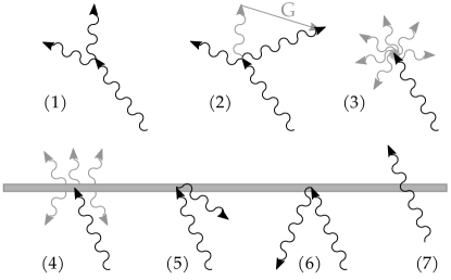
The behaviour of lattice-driven thermal conductivity as a function of temperature has a typical shape which is mostly independent of the material : at high temperature it decreases as , at lower temperature it has a maximum, then going towards zero temperature it decreases sharply to a finite value. The behavior of the lattice thermal conductivity at high temperature is determined by the anharmonic phonon-phonon interactionsPeierls (1955) with a contribution from defects. In the low temperature regime, named after Casimir who studied it in the 1930’sCasimir (1938), thermal conductivity is not a bulk property but it depends on the sample finite size.Casimir (1938)
Theoretical studies of the Casimir regime pre-date the possibility to study thermal conductivity by numerically integrating the phonon anharmonic propertiesCasimir (1938); Berman et al. (1953, 1955). The standard approach consists in modeling the sample boundaries as black bodies that absorb a fraction of the colliding phonons, reflect the rest, and emit phonons to maintain thermal equilibrium. These works use geometric calculations, valid in the linear regime where only the acoustic phonons are taken into account, to predict the low-temperature thermal conductivity, usually with a single free parameter: the surface reflectivity. Invariably they assume a simple geometry for the crystal, such as a long cylinder or a long square parallelepiped with a temperature gradient between its opposite faces; in a shorter cylinder with polished faces the model requires the inclusion of multiple internal reflectionsBerman et al. (1955).
With the arrival of more powerful numerical techniques, it has become more effective to model the surface at the phonon level, as a scattering probability. The probability of scattering from the boundaries can be combined with the probability of scattering due to phonon-phonon interaction in accordance with Matthiessen’s rule.Omini and Sparavigna (1995). This approach has been used in more recent literatureSparavigna (2002) while keeping the assumptions of the long cylindrical geometry, not appropriate for application to thin films, where a temperature gradient can be applied orthogonally to the film lateral extension.
In Fig. 1 we have schematically depicted the possible scattering events responsible for limiting lattice-driven energy flow, we will briefly review them but for detailed discussion we redirect the reader to Ref. Fugallo et al., 2013. Mechanisms (1) and (2) are the intrinsic scattering processes: (1) is the “normal” (N) scattering, it conserves momentum and does not limit thermal conductivy. N scattering is only important at very low temperature (a few K). (2) The umklapp (U) processes, that conserves crystal momentum modulus the addition of a reciprocal lattice vector, are the main limiting factor at high temperature and the prevalent intrinsic scattering mechanism. When studying thermal conductivity in the single-mode relaxation-time approximation (SMA), it is assumed that U scattering is dominant and that the scattered phonons are thermalized, i.e. that on average they are scattered toward the equilibrium thermal distribution. This approximation is very robust and works to within a few percent in a large range of temperatures and materials.Fugallo et al. (2014)
Diagram number (3) depicts the Rayleigh scattering with a point defect, which could be a vacancyRatsifaritana and Klemens (1987), a substitutional defect or isotopic disorderOmini and Sparavigna (1995). Finally, events (4), (5) (6) and (7) are possible interactions between a phonon and the sample boundary: (4) is adsorption and re-emission by the surface; (5) is inelastic reflection by a “white” surface. We remark that, as it has been shown in Ref. Berman et al., 1955, events (4) and (5) are equivalent from a thermal-transport point of view, we will just use (4) from here on. Further on, (6) is elastic reflection, where the momentum component parallel to the surface is conserved but the orthogonal component is inverted. Reflections can limit thermal conductivity in the direction orthogonal to the surface. Finally, in (7) a phonon can cross the boundary without scattering, this is of course not possible if the sample is suspended in vacuum, but can be the case if the sample is composed by multiple mis-matched segments, or if it contains stacking defects.
In order to describe the interface, we introduce three dimensionless parameters: the absorption fraction , the reflection fraction and the transmission , these are the probabilities that a phonon will undergo process (4), (6) or (7) respectively when it collides with the boundary. The condition holds. In general these parameters may depend on phonon energy and its incidence angle, they can be computed using molecular dynamics techniquesAlkurdi et al. (2017). A special limit case is a very rough surface for which .
III.2 Thermal transport in the single-mode approximation
In the single mode approximation (SMA) the thermal conductivity matrix is:
| (2) |
Where is a composite index running over the phonon wavevectors q in reciprocal space and the phonon bands ; are the number of q-points used to sample the Brillouin zone, is the unit-cell volume, is the Boltzmann constant and is temperature. Inside the sum, the composite index stands for the band index and the wavevector ; then is the phonon frequency, is the phonon group velocity; and are cartesian directions () is the Bose-Einstein distribution and is the phonon relaxation time, or inverse full-width half-maximumPaulatto et al. (2013).
The SMA is accurate when umklapp or dissipative scattering is dominant over "normal" and elastic scattering, we have checked that this is always the case in Bi2Se3 above 1 K: above this temperature the exact solution of the Boltzmann transport equation (BTE)Fugallo et al. (2013) only increase by a couple percent. As the SMA equation is much cheaper to compute, easier to manipulate and has a more straightforward interpretation, we will use it exclusively in the rest of the paper.
III.3 Thermal transport in thin film crystals
In order to progress further we have to take into account the real geometry of our sample. In this paper we will consider two cases: (i) a thin film of Bi2Se3 of thickness along direction and virtually infinite in the other two directions with two very rough opposing surfaces; (ii) bulk Bi2Se3 intercalated with partial planes of Bi2, which is a common kind of crystal defect,Eddrief et al. (2014); Huang et al. (2012) at an average distance .
In case (i) we consider a phonon emitted from a surface that moves toward the opposite surface with a component of its group velocity . After a time , the phonon will reach the other surface and be absorbed with probability , giving the first phonon scattering rate and the relaxation time . If it is not absorbed (probability ), the phonon will be reflected back toward the initial surface with identical speed and it will undergo a second absorption/reflection process. The probability of a third reflection is , for the th reflection is is . After summing the geometric series, the total effective lifetime is:
| (3) |
For boundary scattering, conveniently cancels out giving , but we prefer to leave eq. 3 in a general form to consider more general cases. Furthermore, if a phonon is reflected, its velocity component that is orthogonal to the surface will be inverted. We can account for this possibility in eq. 2 renormalizing in the following way: a fraction of the phonons will change the sign of , a fraction of them will hit the opposite boundary, be reflected a second time and change sign again, and so on. The material is traversed in a “flying” time . During this time phonons are scattered at a rate , resetting the process. With being its total (intrinsic and extrinsic) relaxation time. This can be expressed as:
| (4) |
Again, we do not replace with because we want to keep this equation as general as possible.
In case (ii), a bulk material intercalated with planes, the reasoning is very similar, with the caveat that , although for an atom-thin intercalated layer we can safely assume that is almost zero.
The final formula for becomes:
| (5) |
With from eq. 4, and comprises all the scattering terms, summed with the Matthiessen’s rule:
| (6) |
where additional scattering terms like point-defect scattering, can be added. In the case of Bi2Se3 we will see in Sec. V.4 the impact that internally reflected phonon have on the conductivity. We also underline that while our samples are not free-standing in the experiment, we assume that, on the time-scale of the measurements, the transmission of heat from Bi2Se3 to the GaAs substrate can be ignored.
IV Technical details of first-principles simulations
IV.1 Computational method
All calculations have been performed using the Quantum-ESPRESSO suite of codesGiannozzi et al. (2009, 2017), and in particular phDal Corso et al. (1993) and d3qPaulatto et al. (2013) modules. D3q efficiently computes 3-body anharmonic force constants from density functional perturbation theoryBaroni et al. (1987); Giannozzi et al. (1991); Baroni et al. (2001) and the "2n+1" theoremGonze and Vigneron (1989); Debernardi and Baroni (1994). We also used the related Thermal2 codesPaulatto et al. (2013); Fugallo et al. (2013) to compute intrinsic phonon lifetime, scattering with isotopic defectsOmini and Sparavigna (1995) and border effects and to compute lattice-driven thermal conductivity in the single-mode relaxation time approximation (RTA) and by solving iteratively the full Peierls-BoltzmannPeierls (1955) transport equation via a functional minimizationFugallo et al. (2013).
We used the generalized gradient approximation with the PBEPerdew et al. (1996) parametrization. We employed norm-conserving pseudopotentials from the SG15-ONCV libraryHamann (2013); Schlipf and Gygi (2015); Scherpelz et al. (2016), which include scalar-relativistic effects, and custom made pseudopotentials based on the SG15-ONCV pseudisation parameters, but including full-relativistic spin-orbit coupling (SOC). The ph code includes SOC effectsDal Corso (2007), but the d3q code does not, hence we always used scalar-relativistic pseudopotentials for the third order calculations.
We used a kinetic energy cutoff of 40 Ry for the plane wave basis set, and we integrated the electronic states of the Brillouin zone (BZ) using a regular Monkhorst-Pack grid of k-points, except when computing the effective charges and static dielectric constant via linear response, which only converged with a much finer grid of points.
The phonon-phonon interaction was integrated using a very fine grid of q-points, when computing the linewidth along high-symmetry direction or the phonon spectral weight. A coarser grid of points was used when computing the thermal conductivity. The SMA thermal Boltzmann equation was itself integrated over a grid q-points. All the grids in this paragraph were shifted by a random amount in order to improve convergence avoiding symmetry-equivalent points. The finite size effects of section III.3 where included in the calculation of using an in-house OctaveEaton et al. (2019) code available upon request.
IV.2 Simulated crystal structure
Bi2Se3 belongs to the tetradymite-type crystal with a rhombohedral structure (point group Rm, Wyckoff number 166). In the rhombohedral unit cell there are three Se and two Bi atoms. One Se atom is at the (1a) site , the remaining Se and Bi atoms are at the two-fold (2c) sites of coordinates and , with one free parameter for each species, which we indicate as and respectively. Structural parameters obtained from experimental measurement and from ab-initio simulations are shown in Tab. 1. Both the scalar relativistic and the fully relativistic PBE calculations give substantially expanded structures, both in and , as is customary in this approximation. As the electronic band gap is quite sensitive to the geometry, we also calculated the bandgap for the experimental volume. In all fully relativistic calculations the gap is substantially overestimated, in agreement with previous theoretical calculations.
| structure | a (Å) | c (Å) | V (Å3) | gap (meV) | |||
| Experimental: | 4.138 | 28.64 | 422.8 | - | - | 2005 | |
| approximation | structure | a (Å) | c (Å) | V (Å3) | gap (meV) | ||
| this paper: | |||||||
| SR | theoretical | 4.198 | 30.12 | 459.6 | 0.217 | 0.398 | 471 |
| SOC | theoretical | 4.211 | 29.76 | 457.0 | 0.215 | 0.399 | 373 |
| SR | experimentala | 4.138 | 28.64 | 422.8 | 0.211 | 0.400 | 183 |
| SOC | experimentala | 4.138 | 28.64 | 422.8 | 0.209 | 0.401 | 333/444b |
| DFT simulations in literature: | |||||||
| SOC/vasp | experimentalZhang et al. (2012) | 4.138 | 28.64 | 422.8 | - | - | 320 |
Bi2Se3 thin films measured here had thicknesses between 18 nm and 191 nm. The stack of 2 Bi and 3 Se atoms (one Q-layer) is nm thick, which means that even for the thinnest slab we have 18 or 19 Q-layers.
IV.3 Electronic contribution to thermal conductivity
Commercially available bulk Bi2Se3 samples, and our epitaxial Bi2Se3 thin film samples, are always doped to a certain extent by the presence of vacancies and imperfect stoichiometry. For this reason, even if the perfect material is a small gap insulator, we expect to measure a certain amount of electron/hole driven thermal and electric transport. Although there is no simple way to isolate the electronic contribution to thermal transport (), we can estimate it from electric conductivity.
Mobility (), doping and electrical resistivity () of most of the thin films have been measured by conventional Hall bar measurements performed in the plane perpendicular to the trigonal axis, , of Bi2Se3 thin films.
It turns out that, at 300 K our thin films are -doped and present a metallic behavior with a carrier concentration between cm-3, cmVs and mcm. A coarse evaluation of the electronic contribution to the in-plane thermal conductivity, , can be given by using the Wiedemann-Franz law , with ranging between and V2K-2.Navrátil et al. (2004) Consequently, at 300 K ranges between W/mK.
Concerning the out-of-plane resistivity term, , a rough estimation can be given by since such a ratio is found in bulk Bi2Se3Stordeur et al. (1992) leading to between W/mK. It is worthwhile to underline that measurements performed in very thin Bi2Se3 samples (9 QL) give a slight lowering of the resistivity (0.7 mcm), which may be caused by slightly increasing at very low thickness.
V Results and discussion
V.1 Electronic structure
Theoretical lattice parameter: Experimental lattice parameter:


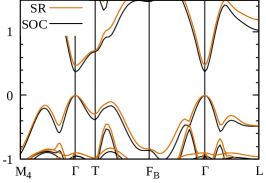


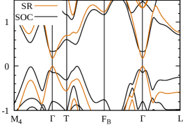
Before delving in the calculation of the vibrational properties, we have taken care to verify that the approximations used to deal with the ab-initio problem are valid. A few potential difficulties have to be accounted for: the first is that Bi2Se3 is a small gap semiconductor, special care is needed in order to prevent the gap from closing. The gap magnitude depends both on the kind of local- or semi-local- exchange and correlation kernels and on the lattice geometry used. In any case, the Kohn-Sham single particle gap is not guaranteed to be correct, as it is not a ground-state property. However, if its character is different from the experimental one it can indicate that the employed approximation is non appropriate. The optical gap has been measured experimentally as being direct and meV wideMartinez et al. (2017).
Another difficulty is treating the inter-layer Van der Waals bond; the inter-layer distances are usually over-estimated by standard local density approaches. However it is possible to improve the agreement with experiment of vibrational frequencies using the experimental lattice parameters. For this reason, we have simulated the electronic structure using both the experimentally measured lattice parameter and the theoretically calculated values. In both cases we optimize the internal degrees of freedom to avoid unstable phonons.
In Fig. 2 we plot the electronic band structure, in a range of a few eV around the Fermi energy. We note that the band structure is very similar except for the case where relativistic effects are included in conjunction with the experimental lattice parameter (Figure 2b). When using the theoretical lattice parameter, (values give in Table 1) the gap is of 471 meV in the scalar relativistic case and it decreases to 373 meV in the fully relativistic calculation. Conversely, if we use the experimental volume and optimize the internal coordinates, the gap is smaller for the scalar relativistic calculation 183 meV (Fig. 2c) while in the fully relativistic case the indirect gap is at 333 meV and the direct gap at 444 meV (Fig. 2d).
V.2 Phonon dispersion
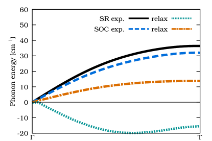
The phonon dispersion does not change dramatically with the different choices of SOC treatment, however we do observe a global, relatively constant, rescaling of the frequencies which can be associated with the difference in the unit cell volume. When not including SOC, if the theoretical lattice parameter is used, the phonon dispersion exhibits negative frequencies. However, when using the experimental lattice parameters, which correspond to a 5% smaller unit cell volume, this instability is removed. Furthermore, if SOC is included, both theoretical and experimental lattice parameters yield stable phonons, as long as the internal degrees of freedom are properly relaxed. Because inter-planes binding is mediated by Van der Waals forces, which usually leads to an over-estimation of the bond length in the PBE approximation, we expect that the modes changing the inter-layer distance will be too soft. For this reason, we show in Fig. 4 the phonon band that is more sensitive to a change in lattice parameter, it is the longitudinal acoustic (LA) mode along the [111] direction which, in the trigonal geometry, is orthogonal to the planes of Bi or Se.
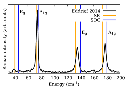
We have compared the phonon frequencies at the point with available data from infrared and Raman spectroscopy, in order to establish which method gives a closer match to the phonon frequencies. These comparisons are summarized in table 2. We note that using the experimental lattice parameter gives a consistently better match for the Raman active modes than using the theoretical one, hence we will focus on the former. The SR calculations slightly under-estimate the phonon frequencies, while with the inclusion of SOC the theoretical frequencies tend to over-estimate the measured ones. SOC is more accurate for the highest optical bands, but less so for the low-energy bands; as the latter are more important for thermal transport, due to the Bose-Einstein factor of eq. 2, we expect that not including SOC may give a better match for the value of . We verified that our calculations at the theoretical lattice parameter agree with those of Ref. Cheng and Ren, 2011.
V.2.1 Effective charges and LO-TO splitting
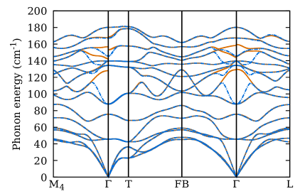
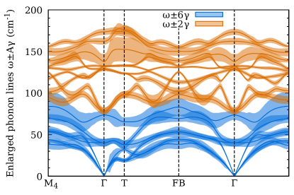
Even high-quality Bi2Se3 single crystals are doped by a relatively large amount ( ecm3) of lattice defects. Below we will see that this doping has no significant effect on the electronic structure nor on the geometry of the crystal, but it is sufficient to effectively screen long-range/small-wavevector splitting of longitudinal and transverse optical modes (LO-TO splitting). In figure 5 we have plotted the phonon dispersion with and without the LO-TO splitting. We can see that a couple of modes are particularly affected. If we number the modes in order of increasing energy, these are the modes 8 and 9 where the atoms move in the plane perpendicular to [111] with Se ions going in the direction opposite to that of Bi ions. These modes are degenerate without LO-TO at an energy of 87 cm-1, but the mode which is aligned with the q-vector jumps to 130 cm-1 when long-range effects are included. When coming from the [111] direction itself, along the - line, the two modes remain degenerate, because the q wavevector is parallel to the polarisation.
| experiments: | ||||||||
|---|---|---|---|---|---|---|---|---|
| IR active (Ec) | Raman active | |||||||
| Symmetry | ||||||||
| Ref. Richter and Becker, 1977 (50 K)a | 61 | 134 | ||||||
| Ref. Richter and Becker, 1977 (300 K)a | 65 | 129 | 72 | 131.5 | 174.5 | |||
| Ref. Eddrief et al.,2014 | 39 | 74 | 135 | 177 | ||||
| simulations harmonic level: | ||||||||
| SR theo. | 76.2-123.8 | 129.7 | 143.4 | 161.2 | 38.3 | 61.8 | 130.5 | 171.5 |
| SOC theo. | 64.7-111.2 | 123.6 | 135.6 | 154.7 | 38.7 | 63.3 | 121.6 | 166.3 |
| SR exp.b | 87.8-129.8 | 134.2 | 145.2 | 166.4 | 45.6 | 75.6 | 139.7 | 180.1 |
| SOC exp.b | 78.0-123.0 | 128.5 | 138.0 | 162.3 | 40.2 | 73.6 | 132.2 | 173.6 |
-
a
Infrared peak position are at 50 K and 300 K respectively.
-
b
Lattice parameters from Ref. Wyckoff, 1963
V.3 Thermal transport in bulk
.
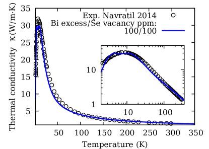
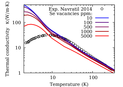
Ref. Wonlinee have initially studied the phonon-driven thermal conductivity in the bulk phase as experimental data are available with good precision over a wide range of temperature. In particular we have taken as reference the data of Navratil and coworkersNavrátil et al. (2004), where they estimate the fraction of lattice-driven and electron-driven transport.
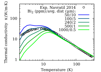
In Fig. 7 we plot the experimental data of the in-plane thermal conductivity measured in Ref. Navrátil et al., 2004, side by side with calculations from 2 K up to 400 K, in the RTA (we checked that the exact inversion of the Boltzmann transport equation yield practically identical values). As it can be seen, the room temperature behaviour of the lattice contribution to is in perfect agreement with our calculation of the intrinsic thermal conductivity. This agreement is possible thanks to the inclusion of lattice defects in the model, as explained in the rest of this section.
Below 20 K, is limited by extrinsic scattering processes such as the scattering with sample borders, with the isotopes or/and with lattice defects. As Navratil et al. used a large mono-crystal, and isotopical effects are negligibles in Bi2Se3,111The relative mass variance of Selenium isotopes is only , while Bismuth has only one stable isotope only lattice defects can explain the low temperature behaviour.
According to literature,Huang et al. (2012) two kind of defects are common in Bi2Se3 crystals: point-defect vacancies of Se, and Bi2 partial-layer intercalation. Each Selenium vacancy contributes around two charges to the total doping, which means that at a doping concentration of around ecm3 the fraction of missing Se atoms is of order ppm. We have simulated this defect concentration using an effective Rayleigh point-scattering model, assigning to each vacancy an effective mass as in Ref. Ratsifaritana and Klemens, 1987. We found that it is far too low to explain the low-temperature drop in thermal conductivity. Even taking an unrealistically high point-defect concentration, such as ppm (5%), the correct curve shape at low temperature is not reproduced. Finally, we remark that using a more accurate, i.e. ab-initio, estimate of the defect cross-section would be equivalent to a change in defect concentration, but would not change the shape of the curve.
On the other hand, if we assume the presence of Bi2 partial layers, we can include it in the simulation using Sparavigna-Casimir scattering theory, i.e. using an effective model that includes a scattering time which is proportional to the ratio between the phonon mean free path and the sample size. We tuned the average inter-defect distance to fit the temperature of maximum , around 10 K. The theoretical position of the maximum is a better fitting parameter than its absolute value, as the latter is very difficult to converge at low temperature in simulations. Notwithstanding that, the calculation reproduces the absolute value quite well, which strengthens the validity of our assumption. In Fig 8, the best agreement is found when the average distance between Bi2 planes is fixed at 5 m. Comparing this value to the size of the unit cell along gives a concentration of excess Bismuth of around ppm, and considering that each additional Bi atom provides three charges, this is compatible with the measured doping concentration.
We note that the effect of Selenium vacancies and Bismuth partial layer intercalation is qualitatively different: a increasing concentration of Selenium vacancies causes a global reduction of , on the other hand increasing the frequency of Bismuth partial layer intercalation moves the maximum of toward higher temperatures, without changing its high-T value. If we combine the two types of defects, we observe that Selenium vacancies have virtually no effect until their concentration is greater than 100ppm, after which scattering from vacancies lead to a considerable reduction in at higher T. As a consequence, the best match remains a concentration of around 100 ppm Bismuth partial layer intercalation with 100 ppm or less Selenium vacancy. This is compatible with the high n-type concentration ( cm-3) of the bulk material measured.
V.4 Thermal transport in thin films
| Thermal conductivity: | ||
| Thickness | Total (measured) | Lattice (estimated) |
| (nm) | (W/mK) | (W/mK) |
| 18 | 0.39 | 0.19 |
| 30 | 0.52 | 0.32 |
| 53 | 0.53 | 0.33 |
| 105 | 0.56 | 0.36 |
| 191 | 0.68 | 0.48 |
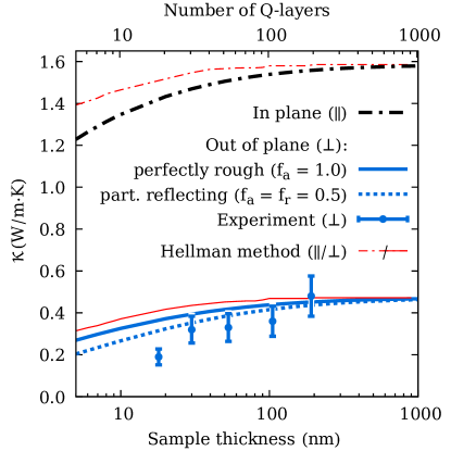
Thermoreflectance measurements provide the total out-of-plane () thermal conductivity which is the sum of the electronic and lattice contributions. As described in section IV.3, we estimate the lattice contribution after measuring the in-plane electronic conductivity in thin films and estimating the out-of-plane electronic conductivity from the measured conductance anisotropy of bulk Bi2Se3.
Transport measurements performed attest that our thin films are doped and present a metallic behavior with a carrier’s concentration bracketed by cm-3, cmVs and mcm at room temperature.
Thus a coarse evaluation of the electronic contribution to the in-plane conductivity can be given using the Wiedmann-Franz law with L the Lorentz number, ranging between 2 and V2K-2. Consequently is bracketed between W/mK.
In table 3 we report the measured values for the total and lattice thermal conductivity, obtained by subtraction the estimated electronic contribution. In Fig. 9, we compare the measured lattice thermal conductivity with the simulations. The agreement is within the experimental errorbar. Including internal reflection effects (dashed line in the figure) does improve the agreement but is not sufficient to explain completely the discrepancy for the smallest slab. This may indicate that a simple Casimir model is not sufficient for such a thin sample, a more detailed description of the interaction of phonon with the surface, including q and dependence could improve the agreement. Finally, the laser penetration depth in the sample (around 10 nm) could play a role for the thinnest slabs, although there is no simple way to include it in the simulation.
We have also tested the approach of Ref. Hellman and Broido, 2014 (red lines of Fig. 9), which consists in cutting off completely the contribution of phonons that have mean free path larger than the sample dimension. The behaviour is relatively similar, but the predicted value of is considerably larger for the smaller samples.
VI Conclusions
We calculate the phonon-component in-plane and out-of-plane thermal conductivity of Bi2Se3 bulk and films with different thicknesses by using the Boltzmann equation with phonon scattering times obtained from anharmonic third order density functional perturbation theory. Our results agree with existing measurements on bulk samplesNavrátil et al. (2004, 2001) and with our room-temperature thermoreflectance measurements of on films of thickness ranging from nm to nm.
The calculated thermal conductivity of bulk Bi2Se3 is in excellent agreement with the experimental data of Ref.Navrátil et al., 2004 at all temperatures. While the high temperature limit (e. g. room temperature) is essentially determined by the intrinsic thermal conductivity, the low temperature regime, in the past attributed to Se vacancy, can be very well accounted for by assuming ppm Bismuth insertion and ppm of Se vacancies. In contrast, Se vacancies alone do not explain the low-T behaviour of the conductivity.
In thin films, we find that the thermal conductivity measured at room temperature, monotonically decreases with reducing film thickness . We can attribute this reduction to incoherent scattering of out-of-plane momentum phonons with the film upper and lower surfaces. Our work outlines the crucial role of sample thinning in reducing the out-of-plane thermal conductivity.
VII Acknowledgements
MC acknowledges support from the European Graphene Flagship Core 2 grant number 785219. Computer facilities were provided by CINES, CCRT and IDRIS (projects 907320 and 901202). MM and DF thank Haneen Sameer Abushammala and Heba Hamdan for assistance at the very beginning of thermoreflectance experiments.
References
- Behnia (2015) K. Behnia, Fundamentals of Thermoelectricity -, 1st ed. (OUP Oxford, New York, London, 2015).
- Dresselhaus et al. (2007) M. Dresselhaus, G. Chen, M. Tang, R. Yang, H. Lee, D. Wang, Z. Ren, J.-P. Fleurial, and P. Gogna, Advanced Materials 19, 1043 (2007).
- Navrátil et al. (2004) J. Navrátil, J. Horák, T. Plecháček, S. Kamba, P. Lošt’ák, J. Dyck, W. Chen, and C. Uher, Journal of Solid State Chemistry 177, 1704 (2004).
- Navrátil et al. (2001) J. Navrátil, T. Plecháček, J. Hork, S. Karamazov, P. Lošt’ák, J. Dyck, W. Chen, and C. Uher, Journal of Solid State Chemistry 160, 474 (2001).
- Hor et al. (2009) Y. S. Hor, A. Richardella, P. Roushan, Y. Xia, J. G. Checkelsky, A. Yazdani, M. Z. Hasan, N. P. Ong, and R. J. Cava, Phys. Rev. B 79, 195208 (2009).
- Uhrer and Morelli (1999) C. Uhrer and D. Morelli, Thermal Conductivity 25 / Thermal expansion 13 (Technomic Publishing, 1999).
- Fournier et al. (2018) D. Fournier, M. Marangolo, M. Eddrief, N. N. Kolesnikov, and C. Fretigny, Journal of Physics: Condensed Matter 30, 115701 (2018).
- Rosencwaig et al. (1985) A. Rosencwaig, J. Opsal, W. L. Smith, and D. L. Willenborg, Applied Physics Letters 46, 1013 (1985).
- Pottier (1994) L. Pottier, Applied Physics Letters 64, 1618 (1994).
- Fabbri et al. (1996) L. Fabbri, D. Fournier, L. Pottier, and L. Esposito, Journal of Materials Science 31, 5429 (1996).
- Li et al. (1999a) B. Li, L. Pottier, J. Roger, D. Fournier, K. Watari, and K. Hirao, Journal of the European Ceramic Society 19, 1631 (1999a).
- Plamann et al. (1996) K. Plamann, D. Fournier, B. C. Forget, and A. Boccara, Diamond and Related Materials 5, 699 (1996), proceedings of the 6th European Conference on Diamond, Diamond-like and Related Materials Part 2.
- Li et al. (1999b) B. Li, J. P. Roger, L. Pottier, and D. Fournier, Journal of Applied Physics 86, 5314 (1999b).
- Pélissonnier-Grosjean, C. et al. (1999) Pélissonnier-Grosjean, C., Fournier, D., and Thorel, A., J. Phys. IV France 09, 201 (1999).
- Frétigny et al. (2012) C. Frétigny, J.-Y. Duquesne, D. Fournier, and F. Xu, Journal of Applied Physics 111, 084313 (2012).
- Eddrief et al. (2014) M. Eddrief, P. Atkinson, V. Etgens, and B. Jusserand, Nanotechnology 25, 245701 (2014).
- Peierls (1955) R. S. Peierls, Quantum theory of solids (Oxford University Press, 1955).
- Casimir (1938) H. Casimir, Physica 5, 495 (1938).
- Berman et al. (1953) R. Berman, F. E. Simon, and J. S. Ziman, Proceedings of the Royal Society of London A: Mathematical, Physical and Engineering Sciences 220, 171 (1953).
- Berman et al. (1955) R. Berman, E. L. Foster, and J. S. Ziman, Proceedings of the Royal Society of London A: Mathematical, Physical and Engineering Sciences 231, 130 (1955).
- Omini and Sparavigna (1995) M. Omini and A. Sparavigna, Physica B: Condensed Matter 212, 101 (1995).
- Sparavigna (2002) A. Sparavigna, Phys. Rev. B 65, 064305 (2002).
- Fugallo et al. (2013) G. Fugallo, M. Lazzeri, L. Paulatto, and F. Mauri, Phys. Rev. B 88, 045430 (2013).
- Fugallo et al. (2014) G. Fugallo, A. Cepellotti, L. Paulatto, M. Lazzeri, N. Marzari, and F. Mauri, Nano Letters 14, 6109 (2014), pMID: 25343716.
- Ratsifaritana and Klemens (1987) C. A. Ratsifaritana and P. G. Klemens, International Journal of Thermophysics 8, 737 (1987).
- Alkurdi et al. (2017) A. Alkurdi, S. Pailhès, and S. Merabia, Applied Physics Letters 111, 093101 (2017).
- Paulatto et al. (2013) L. Paulatto, F. Mauri, and M. Lazzeri, Phys. Rev. B 87, 214303 (2013).
- Huang et al. (2012) F.-T. Huang, M.-W. Chu, H. H. Kung, W. L. Lee, R. Sankar, S.-C. Liou, K. K. Wu, Y. K. Kuo, and F. C. Chou, Phys. Rev. B 86, 081104 (2012).
- Giannozzi et al. (2009) P. Giannozzi, S. Baroni, N. Bonini, M. Calandra, R. Car, C. Cavazzoni, D. Ceresoli, G. Chiarotti, M. Cococcioni, I. Dabo, A. Dal Corso, S. De Gironcoli, S. Fabris, G. Fratesi, R. Gebauer, U. Gerstmann, C. Gougoussis, A. Kokalj, M. Lazzeri, L. Martin-Samos, N. Marzari, F. Mauri, R. Mazzarello, S. Paolini, A. Pasquarello, L. Paulatto, C. Sbraccia, S. Scandolo, G. Sclauzero, A. Seitsonen, A. Smogunov, P. Umari, and R. Wentzcovitch, J. Phys.: Condens. Matter 21, 395502 (2009).
- Giannozzi et al. (2017) P. Giannozzi, O. Andreussi, T. Brumme, O. Bunau, M. B. Nardelli, M. Calandra, R. Car, C. Cavazzoni, D. Ceresoli, M. Cococcioni, N. Colonna, I. Carnimeo, A. D. Corso, S. de Gironcoli, P. Delugas, R. A. D. J. A. Ferretti, A. Floris, G. Fratesi, G. Fugallo, R. Gebauer, U. Gerstmann, F. Giustino, T. Gorni, J. Jia, M. Kawamura, H.-Y. Ko, A. Kokalj, E. Küçükbenli, M. Lazzeri, M. Marsili, N. Marzari, F. Mauri, N. L. Nguyen, H.-V. Nguyen, A. O. de-la Roza, L. Paulatto, S. Poncé, D. Rocca, R. Sabatini, B. Santra, M. Schlipf, A. P. Seitsonen, A. Smogunov, I. Timrov, T. Thonhauser, P. Umari, N. Vast, X. Wu, and S. Baroni, J. Phys.: Condens. Matter 29, 465901 (2017).
- Dal Corso et al. (1993) A. Dal Corso, S. Baroni, R. Resta, and S. de Gironcoli, Phys. Rev. B 47, 3588 (1993).
- Baroni et al. (1987) S. Baroni, P. Giannozzi, and A. Testa, Phys. Rev. Lett. 58, 1861 (1987).
- Giannozzi et al. (1991) P. Giannozzi, S. de Gironcoli, P. Pavone, and S. Baroni, Phys. Rev. B 43, 7231 (1991).
- Baroni et al. (2001) S. Baroni, S. de Gironcoli, A. Dal Corso, and P. Giannozzi, Rev. Mod. Phys. 73, 515 (2001).
- Gonze and Vigneron (1989) X. Gonze and J.-P. Vigneron, Phys. Rev. B 39, 13120 (1989).
- Debernardi and Baroni (1994) A. Debernardi and S. Baroni, Solid State Communications 91, 813 (1994).
- Perdew et al. (1996) J. Perdew, K. Burke, and M. Ernzerhof, Phys. Rev. Lett. 77, 3865 (1996).
- Hamann (2013) D. R. Hamann, Phys. Rev. B 88, 085117 (2013).
- Schlipf and Gygi (2015) M. Schlipf and F. Gygi, Computer Physics Communications 196, 36–44 (2015).
- Scherpelz et al. (2016) P. Scherpelz, M. Govoni, I. Hamada, and G. Galli, Journal of Chemical Theory and Computation 12, 3523 (2016), pMID: 27331614.
- Dal Corso (2007) A. Dal Corso, Phys. Rev. B 76, 054308 (2007).
- Eaton et al. (2019) J. W. Eaton, D. Bateman, S. Hauberg, and R. Wehbring, GNU Octave version 5.1.0 manual: a high-level interactive language for numerical computations (2019).
- Zhang et al. (2012) J.-M. Zhang, W. Zhu, Y. Zhang, D. Xiao, and Y. Yao, Phys. Rev. Lett. 109, 266405 (2012).
- Martinez et al. (2017) G. Martinez, B. A. Piot, M. Hakl, M. Potemski, Y. S. Hor, A. Materna, S. G. Strzelecka, A. Hruban, O. Caha, J. Novák, A. Dubroka, Č. Drašar, and M. Orlita, Scientific Reports 7 (2017), 10.1038/s41598-017-07211-x.
- Wyckoff (1963) R. Wyckoff, Crystal Structures, Crystal Structures No. v. 1 (Interscience Publishers, 1963).
- Chen et al. (2011) X. Chen, H. D. Zhou, A. Kiswandhi, I. Miotkowski, Y. P. Chen, P. A. Sharma, A. L. Lima Sharma, M. A. Hekmaty, D. Smirnov, and Z. Jiang, Applied Physics Letters 99, 261912 (2011).
- Stordeur et al. (1992) M. Stordeur, K. K. Ketavong, A. Priemuth, H. Sobotta, and V. Riede, physica status solidi (b) 169, 505 (1992).
- Cheng and Ren (2011) W. Cheng and S.-F. Ren, Phys. Rev. B 83, 094301 (2011).
- Richter and Becker (1977) W. Richter and C. R. Becker, physica status solidi (b) 84, 619 (1977).
- Note (1) The relative mass variance of Selenium isotopes is only , while Bismuth has only one stable isotope.
- Hellman and Broido (2014) O. Hellman and D. A. Broido, Phys. Rev. B 90, 134309 (2014).