Quasiparticle conductance in Spin Valve Josephson Structures
Abstract
We study the quasiparticle current in clean ferromagnetic Josephson structures of the form , where , , and denote superconducting, ferromagnetic or normal layers respectively. Our focus is on the structure of the conductance as a function of bias , emphasizing the subgap region. We use a fully self consistent numerical method, coupled to a transfer matrix procedure to extract . We choose material parameters appropriate to experimentally realized Co Cu Nb structures. We find a resonance peak structure as a function of the intermediate layer thickness and of the misalignement angle between layers. To understand this resonance structure, we develop an approximate analytic method. For experimentally relevant thicknesses, the conductance has multiple subgap peaks which oscillate in position between low and critical bias positions. These oscillations occur in both and the layer thicknesses. We compare our results with those obtained for the spin valve structures and discuss the implications of our results for the fabrication of spin Josephson devices.
I Introduction
In the continuing search for improved and more efficient computing and memory devices involving spin manipulationtsyzu ; esch , many new possibilities have opened up involving ferromanetic () superconducting () hybrid structures. These devices allow for the manipulation of spin states while taking advantage of the low power consumption in superconducting devices. The fundamental phenomena are proximity effects arising from AndreevAndreev reflection together with, in hybrid samples with a nontrivial magnetic structure, the conversion of singlet Cooper pairs into odd-parityberezinskii ; Halterman2002 triplets, whose existence has been experimentallyKeizer2006 demonstrated. Triplet formation drastically changes the proximity effect since the pairs are transmitted through the electrodes over a much larger length scale. Charge and spin transport are coupled and can be reciprocally manipulated via spin transfer torques (STT) or applied fields. In structures involving two layers, such as hybrids, the misalignement angle between layer magnetizations can be changed experimentallyalejandro . Thus the triplet formation, and hence the proximity effect, depends drastically on (such triplets are precluded when or ) and the equilibrium and transport phenomena involved can drastically depend on such manipulations. Hence, hybrid structures involving either spin valve or Josephson configurations continue to be the focus of intensive workSatchell2018 ; birge2018 ; birge2012 ; birge ; Bergeret2017 .
There is growing interest in using Josephson junctions in digital electronics, such as the Rapid Single Flux Quantum (RSFQ)RSFQ ; RSFQ2 ; Manheimer device, where information is stored and transmitted rapidly via the flux quanta. These devices could be made to be more efficient if one were to trade its transistor components for magnetic memory elements such as the spin valve () Holmes2013 . Most of the focus of recent work on Josephson ferromagnetic junction devices has been on the current-phase relationshipRyazanov2001 ; Kontos2002 ; birge2018 ; Maekawa ; hvw15 . The relative phase of the superconductors, at zero current, is either or . For the Josephson structures, the equilibrium state can be changed between the and state by varying the thickness of the ferromagnetic layer hv2004 or the relative magnetization angle hvw15 . In addition, the critical current is also oscillatory with the layer thickness and exchange field strength Buzdin1982 ; Buzdin1991 . However, there are other important aspects of the Josephson structure that are independent of the phase. In this paper, and following up on previous work on the valve configurationwvhg ; Moen2018 ; condpaper ; spinsplitpaper , we focus on the quasiparticle current in the Josephson structures.
The most prominent phenomenon in Josephson structures is of course the Josephson current, the existence of supercurrents in the presence of a non-superconducting junction. In ordinary Josephson junctions there are two Josephson effects: the DC effect and the AC effect Josephson . In the DC effect, an applied DC current runs through the Josephson junction at zero bias, up to a critical value, via the tunneling of the Cooper pairs. The AC effect describes the AC current driven by an applied bias with frequencies in the GHz range for an applied bias of order eV Kittel . In general, the Josephson current is not the only current that runs through a Josephson junction, as there is also the contribution of normal electron transport. In the two-fluid model, we can express the net current in a Josephson structure using the Resistively and Capacitively Shunted Josephson (RCSJ) model RCSJ as:
| (1) |
This equation describes a resistive and capacitive circuit element running in parallel with a pure Josephson junction of tunneling Cooper pairs. This is a non-linear equation and will result in a hysteresis Orlando in the current vs voltage (I-V) curves if the time scale of the RC element is greater than that of the Josephson junction where is the normal resistance of the junction. The term is known as the quasiparticle current and represents the contribution due to normal electron transport. It can be characterized via the conductance, . One can measure the quasiparticle current by shunting the junction. This leaves a hysteretic I-V characteristic at very low biases where the “capture” current is small (and the minimum nonzero voltage is small) in the DC Josephson effect for decreasing current. In the case of a non-tunnel junction, such as a clean or weak-link junction, there may exist unique subgap conductance features. A metallic weak-link is an structure in which the Josephson junction is separated by a thin metal, sometimes the same material as the superconductor. For example, a point contact may be formed with one superconductor in contact with a superconducting substrate. Another example is the microbridge, where a thin bridge is etched between two superconducting “banks” Orlando . Although continuously connected, the intermediate region in each case is considered a normal metal constriction. This is because the constriction is smaller than the coherence length () which destroys superconductivity within the region. These constrictions are therefore studied in the dirty limit Parks . In the clean limit theory, the transport properties are not affected by a constriction or by impurity scattering Orlando .
Here we wish to study the quasiparticle current in the clean limit for structures using a self-consistent method which we present below. For such structures, the standard DC Josephson current has a more complicated form than the simple structure of Eq. (1). Assuming a fixed phase difference , the structure of that term has been previouslyhvw15 studied. Here, however, we are particularly interested in the subgap structure of the quasiparticle current, as described by the conductance .
In 1969, L. J. Barnes discovered multiple conductance peaks within the subgap bias region, using superconducting Nb point contacts Barnes . In these Josephson structures, the subgap region is considered to be any bias below (or in the case of two different superconductors). Barnes found conductance peaks for values of the bias of approximately where is an integer. This subgap structure (SGS) has since been verified in other experiments on metallic weak-link junctions Hansen ; Baturina ; Giubileo . In 1982, Blonder, Tinkham, and Klapwijk (BTK) determined btk how Andreev reflections change the conductance features of an heterostructure where in the subgap region ( in this case) the conductance may be twice that of the normal conductance. For nonzero interfacial scattering, this leads to peaks in the conductance at the critical bias (). This peak represents the increase in energy needed for an electron in the normal metal to transport into the superconductor just above the superconducting energy gap, where the density of states is the highest. For biases less than the gap potential, the right-moving electron will instead Andreev reflect as a left-moving hole. In 1983, Octavio, Blonder, Tinkham, and Klapwijk (OBTK) described the phenomenon known as multiple Andreev reflection (MAR) OBTK . In a superconducting junction that is biased between the two superconductors, an electron leaving the left superconductor will gain in energy before impinging on the right superconductor. If the energy is lower than the gap, it will reflect as a hole which then gains energy before impinging on the left superconductor. This process repeats itself until the original electron has gained enough energy to escape the gap, making multiple reflections in the process. There is thus a peak in conductance when the number of reflections times the bias applied is equal to the energy gap . OBTK went on to describe the subgap structure in junctions via the MAR, although what they find are peaks in the resistance for non-zero temperatures and/or non-zero scattering at the interfaces. One important distinction is the plane wave assumptions of the clean limit theory as opposed to diffusive theory describing the weak-links. In Ref. OBTK, , plane waves were used to describe the reflection coefficients at the interfaces, but no interference of the reflected waves from each interface was included. In general, the plane waves may interfere upon multiple reflections which would diminish the subgap structure. However, as with any junction, there are quantum resonance effects due to the finite thickness of the layers separating the superconductors. There are alsolu2019 spin effects in the MAR spectrum. In addition, OBTK assume a non-self-consistent pair potential, and we have showncondpaper ; spinsplitpaper that a self-consistent pair potential is necessary to accurately describe transport wvhg ; condpaper ; spinsplitpaper ; Moen2018 . Other theoretical work on MAR in weak-link metallic junctions Kummel ; Cuevas has been in the dirty limit Anderson ; Gorkov ; Usadel . We study these reflections and the resulting interference and resonance phenomenon in our ballistic, self-consistent theory for the ferromagnetic Josephson structure.
In previous workcondpaper ; spinsplitpaper we have studied the quasiparticle transport in superconducting spin valve structures (). In these structures, the singlet Cooper pair correlations are short-ranged and oscillatory within the ferromagnet Buzdin1990 ; Halterman2002 . The presence of a second ferromagnet allows for the formation of induced same-spin triplet correlations of the Cooper pairs which are long ranged within the ferromagnet bvermp ; Eschrig2008 ; leksin ; Bergeret2007 ; kalcheim ; singh ; ha2016 . Due to this, and the oscillatory nature of the singlet pair, we found that the subgap features of the system are highly dependent on the magnetic misalignment angle and the thickness of the layer. In Ref. condpaper, we found that the critical bias (CB), i.e. the bias value equal to the saturated pair potential , was spatially and angularly dependent. In Ref. spinsplitpaper, we saw that the conductance features are spin-split between contributions from incoming spin-up and spin-down electrons where, in the subgap region, one spin-band features a peak in conductance while the other spin-band has a minimum. This lead to a peak conductance that is oscillatory with between zero and the critical bias. It was also shown that these conductance features were highly dependent on the interfacial scattering. In fact, nonzero scattering is paramount to the formation of conductance peaks. These dependencies also apply to the system, and we will study the thickness and angular dependence in the results of this work.
In Sec. II, we review our methods, which are the same as those used in Refs. condpaper, and spinsplitpaper, , to study the spin valve Josephson structure. In that section, we also review our analytic approximation of the system to determine the relationship of the electron-hole resonance in and multilayers with interfacial scattering due to a normal metal contact. In Sec. III we present our results, starting with our approximate analytic calculations on the simple and models, before moving on to the fully self-consistent, numerical calculations of the heterostructure. In all our calculations, we determine the thickness dependence of the (or ) layer in relation to the resonance effects determined in Sec. II.3. In addition, we determine the angular dependence for our numerical calculation. We find that the angular dependence is different from that found in the systems previously studied. We present our results for two sets of interfacial scattering parameters: clean interfaces and imperfect interfaces. We also consider nonzero scattering due to a normal metal contact. Finally, we summarize our results in Sec. IV.
II Methods
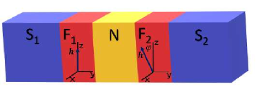
II.1 Self-consistent calculation of the pair potential
The methods in this section are very close to those used in the Refs. wvhg, ; hvw15, ; condpaper, ; spinsplitpaper, (and references therein) for the calculation of the pair potential, and those used in Refs. wvhg, ; condpaper, ; spinsplitpaper, for calculating the conductance. The primary difference is the inclusion of the second superconducting layer. The geometry we consider is depicted in Fig. 1. The layers are assumed to be infinite in the transverse direction (- plane) and the quasiparticle current is along the axis. The eigenvalue equation for the multilayer, in the quasi one-dimensional geometry considered here is:
| (2) |
where is the usual single particle Hamiltonian with interfacial scattering where is the barrier strength at the th interface located at . Also, is the transverse kinetic energy, is the exchange field within the ferromagnetic layers, and is the pair potential within the superconducting layers. Each element in the matrix equation is implicitly a function of the position () within the multilayer. The form of the Hamiltonian is the same as was given in previous workwvhg ; hvw15 ; condpaper ; spinsplitpaper and, because of the presence of two superconductors we, must keep in mind thathvw15 the pair potential is not necessarily real: there may exist a phase difference between the two layers, and we have therefore introduced the complex conjugate of the pair potential . With a single superconductor, there is only one phase associated with the s-wave symmetry and thus the pair potential can be taken to be real. Using our self-consistent method, as described in the above references, we initialize the pair potential within each layer to a selected starting phase difference, and where is the value of for values within the layer, and similarly for . We assume here that the two superconducting layers are made of the same material. We then solve the eigenvalue Eq. (2) and then evaluate the self consistent equation,
| (3) |
where is zero except in the layers and the sum is over all eigenstates with energies less than from the Fermi level. We iteratively solve for by cycling through Eqs. (2) and (3) The phase of the complex pair potential will also iterate using this method. For the equilibrium calculation (zero current), there are always two local stabilities in the phase: and . For an initial guess where the phase difference is not equal to or , the final self-consistent phase will always converge to the value which minimizes the free energy. This value is dependent on the thickness hv2004 and relative magnetization angle hvw15 of the ferromagnets. In non self consistent calculations (such as our approximate analytic calculations below), the and phases are degenerate, and thus we leave the phase to be zero. In our numerical, self-consistent results presented, the overall phase corresponding to the plot displayed is that which minimizes the free energy, i.e. the equilibrium phase. The self-consistent method is necessary to preserve the fundamental property of charge conservationbagwell ; sols2 ; sols ; baym , as explained in Ref. condpaper, .
Using this method, it is possible to allow for two different superconductors () where the coherence length is different for each layer. We focus our attention here to the case in which the two superconductors are made of the same material. This does not mean that the pair potential will be symmetric or have the same magnitude in each layer, as the proximity effect does not impact both superconductors equally as we vary the layer thicknesses. The same asymmetry occurs if one varies the thickness of the individual layers.
II.2 Quasi-particle Conductance
In the previous subsection, we reviewed the determination of the equilibrium properties of the system, in particular the spatial dependence of the pair potential. Now we explain our methods for calculating the conductance. Basically, we use here the same BTK btk method to calculate the conductance as in previous workcondpaper ; spinsplitpaper . Hence, we will not repeat any of the details here. In the BTK method one calculates the conductance from the reflection amplitudes of the spin-dependent ordinary () and Andreev () reflection amplitudes within the left-most layer. In order to simplify our calculations, we introduce a thin normal metal contact, denoted by ’’, located to the left of the layer (see Fig. 1). This makes the ferromagnetic Josephson structure effectively . This contact layer is taken to be thin enough to not affect the calculation of the pair potential through the proximity effect. For this reason, it is not necessary to include it in the equilibrium calculation above. We further explain our reasoning for introducing this contact below. We determine the reflection amplitudes by writing the incoming wavefunctions using these amplitudes and applying the boundary conditions at the end layers and the continuity conditions at the interfaces. If a spin-up incoming electron in the left-most layer is traveling in the normal metal contact , the incoming wavefunction is:
| (4) |
and for a spin-down incoming electron:
| (5) |
where the second spin index of the reflection amplitudes denotes the spin of the incoming particle and is the normal metal wavenumber. The continuity condition of the wavefunctions at each interface can be represented by a matrix equation where and are the wavefunction coefficients of the th layer evaluated at the right and left interface respectively, and is the vector of the reflection/transmission amplitudes. At the layer, this equation becomes where is the vector of the incoming spin electron coefficients. The wavefunctions are described in Ref. condpaper, for the ferromagnetic () and superconducting () layers. The addition of a second superconducting layer is straightforward as one uses the same self-consistent approach as for one layer (see Ref. condpaper, ).
The conductance is then calculated via the BTK method, in the low limit, using (see e.g. Eq. (10) of Ref. spinsplitpaper, ):
| (6) | ||||
where the index refers to the leftmost layer. is given in the customary natural units of conductance . The factors take into account any possible different density of incoming spin up and spin down states. The energy dependence of arises from the applied bias voltage . We measure this bias in terms of the dimensionless quantity where is the value of the order parameter in bulk material. In general one has for the wavevectors:
| (7) |
where for up (down) spins, and is the wavevector corresponding to energy and the internal field of the leftmost layer. All wavevectors are in units of and all energies in terms of . The presence of the normal metal contact means that we can describe the left-most layer using incoming electrons and holes, as opposed to the electron-like and hole-like quasiparticles of the superconductor (see e.g. Ref. btk, ). Hence are actually spin independent, and . Although a description using incoming electron/hole-like quasiparticle amplitudes has been used in studies on the phase relationship in Josephson structures Furusaki , this approach is not well suited for determining the transport properties within the subgap region as these amplitudes can not describe excitations with a subgap energy – only energies above the gap. To probe the subgap energies means describing incoming Cooper pairs instead of the excitation amplitudes. With the layer we are able to describe the quasiparticle states for the subgap in terms of the incoming electron/hole excitation amplitudes. In addition, in the BTK method (see Eq. (6)), is described via the reflected electron and Andreev reflected hole amplitudes. To describe the system using the electron-like and hole-like quasiparticle reflection coefficients would require an entirely new formalism. Adding a normal metal contact is also justified on the basis that experimental systems have contacts from which measurements are made. In addition, we can study the effects of the interfacial scattering due to imperfect contact interfaces. The introduction of a scattering interface allows for multiple Andreev reflections in both single superconductor heterostructures and the Josephson structures, the results of which are conductance peaks in the subgap region sometimes known as the subgap structure (SGS).
II.3 Analytic Approximation
We use also in this paper an analytic approximation. Its purpose is to provide some physical intuition and a quantitative description of the finer details in the full numerical results. To do this we start with a simple model (see Figs. 2 and 3) and go on to a ferromagnetic Josephson structure with normal metal contact (see Figs. 4 and 5). To make our calculation analytic, we need to make many approximations: we assume a one-dimensional (as opposed to quasi-one dimensional) system with infinite layer thicknesses at the left and right ends. Therefore, the only thickness dependencies come from the intermediate layers and . We must assume also a non-self consistent pair potential where is a constant for both the single and Josephson structures. The calculation of the conductance is then a simpler version of that in the numerical calculation. The reflection amplitudes can be solved for using in the case and in the case with normal contact . The matrices are obtained just as the matrices below Eq. (5) from the continuity conditions, of which now there is only at each interface. This can be extended to the case of an intermediate normal metal instead of a ferromagnet simply by taking the exchange field to be zero.
The conductance is then calculated via the BTK method and Eq. (6). The analytic solution involves inverting multiple matrices (which can be done simply using Mathematica). However, the full solution is lengthy, excessively inscrutable and can not be simplified easily. Despite having an analytic solution, the form of the conductance is still complicated due to the sheer number of plane wave combinations of the coefficients that are present in each reflection amplitude. Therefore, we do an analysis similar to that in Ref. spinsplitpaper, for the system by considering some of the possible relevant plane wave combinations to extract periodic behavior. In that work we found that the reflection amplitudes have a periodicity of (in dimensionless units) on the thickness of the layer. This lead to a periodicity of the conductance peak position of , with the subgap peak conductance oscillating between the zero bias and critical bias for increasing thickness of the layer. However, there is another plane wave combination we should consider which describes the SGS for .
Below, and in the rest of the paper, we denote dimensionless lengths by capital letters, e.g. . Consider first an system (for example, a normal metal contact coupled to an bilayer). If there is an interfacial scattering barrier at the interface, it is possible for the Andreev reflected holes from the interface to interfere with the reflections at the interface. We may look for resonance effects in the system by examining the plane wave combination at the critical bias . The wavenumber in the normal metal is then
| (8) |
The combination is in resonance when where is the integer of the harmonic resonance. Thus, the resonance in the amplitudes is expected to occur for
| (9) |
where the normalized pair potential is related to Kittel ; BCS the (dimensionless) coherence length by . The conductance is proportional to the absolute square of the amplitudes, thus the periodicity in the conductance peak resonance occurring at the critical bias should be
| (10) |
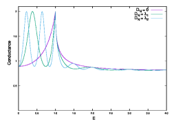
In Sec. III.1 we will discuss (see Fig. 2) the calculated conductance for varying thicknesses . We will see that the periodicity describes the formation of new peaks at the critical bias, shifting the previous numbered peak into the subgap. This resonance is the result of multiple Andreev reflections, where an electron/hole is Andreev reflected off the layer and is again reflected at the interface. The integer is the harmonic of this resonance effect. For , there is an additional oscillatory behavior due to the spin-split effect described in Ref. spinsplitpaper, , which we discuss in Sec. III.1 as well (see Fig. 3).
In the Josephson structure , the additional layer leads to another layer thickness dependence on the conductance. Andreev reflected electrons and holes from the interface may be Andreev reflected again at the interface. If we again consider a normal metal contact with interfacial scattering at the contact, the quasiparticles which transmit through the layer may also reflect at the contact. The net result is a complex resonance effect that can be divided into two parts: resonance from reflections at the interface and from refections at the boundary. We do not have a simple argument for the exact resonance behavior and use a phenomenological approach. We first assume a resonance effect similar to Eq. (10). Then, we introduce a term to take into account the actual computed dependence of the resonance on . We find two harmonic resonance effects on , labeled as the even and odd harmonics:
| (11) |
where we find that approximates the resonance values. The even terms are due to reflections at the interface and have the same form as Eq. (10) while the odd terms are due to reflections at the contact interface. The odd resonance values are reduced by a term which depends only on the ratio . A new peak forms at the critical bias for , shifting lower order harmonic peaks to lower bias, into the subgap as increases. These peaks are equally separated between even/odd pairs for constant . We study these peaks for multiple harmonics in the case and the case in Sec. III.2, see the discussion below associated with Figs. 4 and 5.
We will not consider the higher harmonics () when using our numerical method. This is for two reasons: first, the peak positions are much more difficult to predict as the saturated pair potential (or the “effective” coherence length ) is not constant as one varies layer thicknesses due to the proximity effect. Second, the harmonic occurs for very large intermediate thicknesses: about five times the coherence length of the superconductor. The ballistic nanostructures we wish to study (those built by experimentalists) typically have a total intermediate thickness less than or on the same order as the coherence length. By introducing ferromagnets we can probe the higher harmonic peaks at lower intermediate thicknesses due to the oscillatory behavior of the peaks. We present analytic results in Sec. III.2 and numerical ones in Sec. III.3 for the ferromagnetic Josephson structure.
III Results
In this section we present our results on the conductance in the ferromagnetic Josephson structures ( and ). Preliminarily to our numerical results, we will consider a simplified model of the structure, which can be treated analytically, and work our way up to the structure. Although this model is quantitatively inaccurate, it does help highlight the qualitative features of the subgap conductance in a more intuitive manner. This qualitative understanding is very useful when describing the fully self-consistent numerical results of the structure. We include a normal metal contact as discussed in Sec. II.2, in all our results on Josephson structures. In our numerical results, we determine their dependence on the thickness of the layer as well as on , the misalignment angle of the layer magnetizations. The thickness dependence will be described in relation to the analytic results.
Our results are parameterized by the layer thicknesses and the coherence length of the superconductor. As mentioned above, length scales are all normalized to , the Fermi wavevector of the superconductor. All energies are understood to be normalized to except the dimensionless bias , which is is normalized to the bulk pair potential . The conductance is in units of . The interfacial scattering barriers are normalized by . In each figure below, we take the scattering at the left-side contact interfaces (, , and ) to the intermediate value, . This barrier enhances many of the subgap conductance features by making the peaks sharper and we believe it better represents a realistic experimental situation. In the numerical results, we also consider ideal contact interfaces for comparison. In the analytic results we assume no interfacial scattering at the and interface, for simplicity, but in the numerical calculations we consider both zero and non-zero interfacial scattering at the intermediate interfaces. We take the normalized ferromagnetic exchange field to be , and the dimensionless coherence length to be for each ferromagnetic and superconducting layer respectively. These values have been found to be suitable to describe experimental samples using cobalt and niobium alejandro .
III.1 N′/N/S and N/F/S analytic results
We start our discussion with the analytic results (see Sec. II.3) for and structures. In Fig. 2 we plot the conductance of an multilayer for layer thicknesses such that and a single barrier at the interface. This interfacial scattering is representative of an imperfect metallic contact interface, but it is still far from the tunneling limit. The left- and right-most layers ( and ) are infinite in thickness in the analytic approximation. The thicknesses are the resonance values found in Eq. (10) and represent the interference of the Andreev reflected electrons and holes with those reflected at the interface. The case is equivalent to the system studied by BTK. As seen there, the effect of the barrier decreases the conductance in the subgap region (and at the high bias limit) without decreasing the conductance at the critical bias (CB) . This leads to a sharp peak in the conductance. As the thickness increases, the critical bias peak shifts into the subgap region and a new peak is formed at the CB when reaches a resonance value. Increasing further, other peaks form, shifting the previous peaks further towards zero bias, for each resonance value. We see that the peaks are evenly spaced for each thickness plotted. Also, we see an additional oscillatory behavior in the conductance just above the critical bias. This oscillatory pattern decays at the same rate as in the case () towards the normal conductance. The frequency of the oscillations is proportional to the harmonic of the layer thickness resonance. The thicknesses of the intermediate layer depicted in Fig. 2 are quite large, about five times the coherence length of the superconductor for and ten times for . This makes the results less relevant to the experimental nanoscale heterostructures that we have in mind, where the intermediate layer thicknesses are on the order of the coherence length or less. However, this analytic calculation provides an excellent illustration of the subgap peak structure. We will see that this structure plays a prominent role in ferromagnetic Josephson structures .
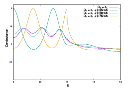
In Ref. spinsplitpaper, we discussed the spin-split conductance for the superconducting spin valve (). There we also used a similar analytic approximation for the model, although only for small thicknesses . We found that the peak conductance oscillates between the critical bias and near zero bias with increasing thickness. This is due to the spin-split conductance: the conductance features differ for incoming spin up and spin down electrons. From our analysis we found the wavelength of the oscillations to be . For these small thicknesses, there is only one resonance peak, attributable to the harmonic. In Fig. 3 we plot the conductance for the system, but for values close to the resonance thickness. The periodicity of the spin-split conductance peak is significantly smaller () than the resonance thickness ( as mentioned above). We plot in Fig. 3 one full period of the spin split oscillation. We see that the conductance oscillates between two different two-peak states: one with the peaks located at the CB and at lower bias, near the middle of the subgap, and one with the peaks located from near zero bias and right to the middle of the subgap. As the thickness increases, the set of two peaks oscillates between low biases and the critical bias, as is the casespinsplitpaper for small thicknesses. Between these states, each peak splits into two, which corresponds to the subgap peaks found in the small case, and features a cusp peak near the CB. These subgap peaks are a split of the two resonance peaks for the first () harmonic. Because this oscillatory behavior effectively shifts all resonance peaks further into the subgap, it is possible to have multiple subgap peaks for thicknesses less than the first harmonic resonance thickness as the higher order resonance peak will shift from the CB into the subgap region. However, the thickness must still be much larger than the coherence length to see this effect in systems.
III.2 S/N/S and S/F/S analytic results
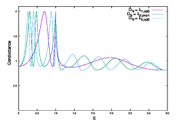
We now turn our attention to analytic results for and Josephson structures. In Fig. 4 we plot the conductance for the structure with and resonance values of the layer thickness (Eq. II.3). The interfacial scattering at the contact is . As discussed in Sec. II.3 the Josephson structure has two sets of resonance values on : the “even” and “odd” resonances. The even resonances are the same as for the case, but the odd resonances have an extra term (see Eq. II.3) that decreases the resonance thickness for the odd harmonics (from to ). This split in resonances is due to the difference in the reflections at the and the interfaces. The exact form of the additional term was not determined, but from analyzing results such as those shown in Fig. 4 we were able to estimate the value of as in Eq. (II.3). We plot a range of thicknesses which include the first two odd resonances () as well as the even resonance. As increases, we see the same shift of the critical bias peaks into the subgap region. However, due to the dual resonance structures, these peaks are not evenly spaced. Furthermore, the oscillations above the gap are not in phase and the frequency is not directly proportional to the harmonic for the odd resonances.
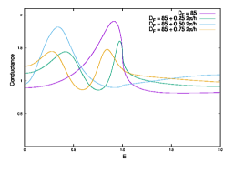
In Fig. 5 we plot the conductance for the structure in our analytic approximation. We have previously establishedspinsplitpaper that the conductance peak is oscillatory between low biases and the CB for varying thicknesses in structures. In the previous subsection, we have shown that this extends to all resonance peaks. We now do the same analysis for the ferromagnetic Josephson structure. We see an oscillatory behavior due to the spin-split conductance that is similar to that in the case, except that the total periodicity is now . We have set the minimum thickness to be which is less than the first resonance value (). This is for two reasons: First, this value is the minimum total thickness of the intermediate layers (between and ) in our numerical calculations on the ferromagnetic Josephson structure. Second, we wish to show how the oscillations of the resonance peaks can shift a higher order harmonic peak into the subgap region, allowing for multiple subgap peaks. Indeed, in Fig. 5 we see a single conductance peak at . As increases, it splits into two subgap peaks (with one being very near the CB). Then, the two peaks reform at into a single subgap peak. Increasing further, this peak splits into two subgap peaks with one being at very low biases. This is quite different from what was found in the structure. Not only is the overall periodicity of the behavior doubled, but here there may exist multiple, distinct subgap peaks instead of a single peak and a cusp at the critical bias. This occurs for realistic thicknesses of the intermediate layers, at least in our analytic approximation. In the next subsection, we analyze the fully self-consistent structure.
III.3 Self-consistent, numerical results for the S1/F1/N/F2/S2 conductance: F2 layer thickness dependence
Through our approximate analytic study, we have found that there are two sources of resonance in the Josephson structure that give rise to conductance peaks in the subgap region. Furthermore, these peaks are oscillatory with increasing thickness of the layer. We now discuss the numerical results of the ferromagnetic Josephson structure . We include a thin normal metal contact which allows us to simplify our methods as explained in Sec. II.2, the structure being then . We will consider both zero and nonzero interfacial scattering at the contact, and we compare the dependence of the conductance on the and interfacial scattering. In numerical calculations, the pair potential within each superconductor is a function of position within the multilayer, as determined by our self-consistent method. Furthermore, in the numerical calculation, all layers are finite in width. We keep all layer thicknesses constant except the layer: , and . The normal metal contact thickness is . We set again and . Our results focus on the quasiparticle current, and do not reflect the zero bias current due to the Josephson effect. Therefore, in interpreting our results, it should be noted that the ultra-low bias conductance may be inaccessible in experiment, even with a hysteresis current from a shunted Josephson circuit, due to the Josephson current.
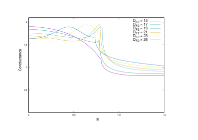
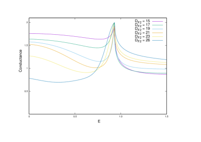
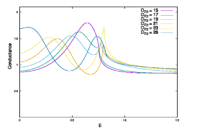
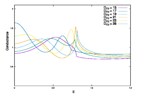
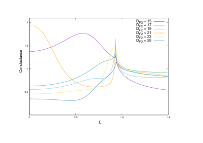
In this subsection, we determine the dependence of the conductance features on . The magnetization of the ferromagnetic layers are assumed to be parallel (). In Sec. III.4 we will consider the dependence of on the misalignment angle at fixed . We consider several sets of interfacial scattering strengths. The interfacial scattering strengths are indexed from the far left to the right starting from zero () thus the barrier strength is , the interfacial barrier strengths are and , and the barrier strengths are and . The barrier strengths are either zero or . We do not consider the situation with all transparent interfaces, i.e. , as this leads to minimal subgap structure and it would be quite unrealistic experimentally.
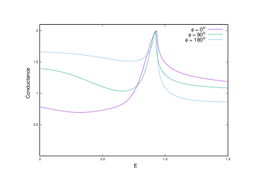
In Fig. 6 we study the conductance dependence for a transparent interface (). It has two subfigures: (a) with interfacial scattering, , and (b) with interfacial scattering, . Conversely, in Fig. 7 we consider the effect of interfacial scattering at the contact interface, , in three subfigures (a) no additional barriers, (b) interfacial scattering, and (c) interfacial scattering. In both of these figures we plot the dimensionless conductance for and varying . In Fig. 6(a) we see in the subgap region a single peak structure, where the peak of the conductance moves from low bias to the critical bias over the range of shown. This single peak structure is similar to that studied in Ref. spinsplitpaper, in which a subgap peak was shown to oscillate in bias position with the ferromagnetic layer thickness in spin valve structures which also had interfacial scattering at the interfaces. The periodicity of the oscillations was shown to be . When the peak is located between zero bias and the critical bias, there is a cusp feature in the critical bias conductance. In subfigure Fig. 6(b), where we plot the conductance for nonzero scattering, we see a very different phenomenon: there is now a subgap minimum as opposed to a subgap peak. There is a marked peak at the critical bias. The subgap minimum is also dependent on . We see that the subgap minimum goes from being near the critical bias at to being near zero bias at . This thickness dependence is different from the oscillatory peak structure in Fig. 6(a); the periodicity of the minima is not . This minimum, or dip structure is not unprecedented. In Ref. OBTK, , a subgap peak structure is found in the resistance when considering nonzero interfacial scattering at the interfaces in Josephson junctions. This translates to dips in the conductance.
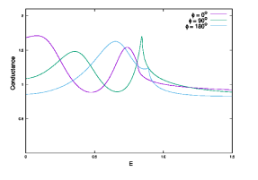
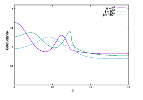
In Fig. 7 we plot the conductance with a nonzero barrier at the interface . The results are more qualitatively similar to the analytic results presented in Sec. III.2. From to the behavior of with bias changes from a single peak near the CB to a two-peak structure, one at low bias and one just below the critical bias. As increases from , we see the single peak shift into the subgap region until a second peak forms at the CB at around . The thickness difference between and is about , which is one quarter of the total oscillatory pattern (see Fig. 5 for comparison). This means the periodicity is doubled by the presence of the layer. This is due to the reflections at the interface which form a second resonance effect as described in Sec. III.2. Comparing Figs. 7(a) and 7(b), we see the effect that the barriers have on the conductance. We observe that the phase of the oscillatory spin-split behavior shifts slightly and the conductance decreases. The subgap peak structure is not enhanced by the barriers, but instead the conductance is decreased in all peak values. The biggest change occurs when we shift focus to the barriers in Fig. 7(c) where the subgap sctructure is much more complicated: there is no subgap peak, except at and , but there is a noticeable inflection point in the subgap at the other thicknesses. We ascribe this to the combined effect of the peak structure we see in Fig. 7(a) and the dip, or minima structure we see in Fig. 6(b). The presence of the barriers forms dips while the barrier provides a peak resonance in the MAR. These two effects do not share the same periodicity with the thickness, which complicates the overall effect. From this we conclude that the barriers have the most impact on the subgap structure. The barrier is also important as it leads to a resonance effect in the MAR which can lead to a second conductance peak or a complex inflection structure within the subgap, depending on what other barriers are in play.
III.4 Self-consistent, numerical S1/F1/N/F1/S1 conductance: angular dependence
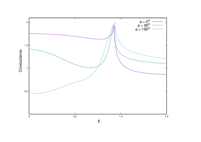
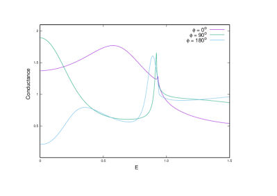
Much of the interest in the spin-valve Josephson structure arises from its putative capability to store information in the relative orientation of the magnetization in the layers. The angular dependence of the conductance constitutes a valve effect in the system. In the superconducting spin valve structure () studied in Ref. spinsplitpaper, , we found a large valve effect in the subgap conductance for certain thicknesses of the layer. We aim here to determine the angular dependence of the structure and the viability of the valve effect found. To do this, we analyze for two of the thicknesses plotted in Sec. III.3, and . We choose these two thickness values because they are separated by a value of , one quarter of the full periodicity with and half the full periodicity for . We will then compare the angular dependence of with the spatial dependence found in Figs. 6 and 7. For each thickness, we will study the case (Figs. 8 and 10) and the case (Figs. 9 and 11). Then, within each figure we compare the effects that the other interfacial barriers have on the angular dependence of the conductance.
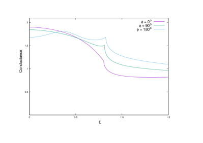
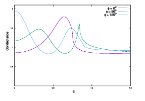
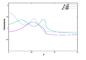
In Figs. 8 and 9 we plot the conductance for and display its dependence. The results are the same as those in Figs. 6 and 7 respectively. In Fig. 8(a) we plot the conductance for . We see a peak in the conductance at low bias for which then transitions to a subgap peak at . This is reminiscent of the thickness dependence, where the single low bias peak at transitions into a subgap peak at in Fig. 6(a). This parallel extends to the case in Fig. 8(b). At there is only a small dip in the conductance near the critical bias. At the low bias conductance drops to a minimum value, similar to the case in Fig. 6(b). However, in addition to the dip structure, there appears to be a small inflection near which was not seen for in the case. This feature is more similar to those found in Fig. 7(c).
In Fig. 9(a) we see a single-peaked conductance at . At the single peak splits into a subgap peak and a CB peak. Then, at , the conductance has two subgap peaks, one at low bias and one just below the critical bias. This angular dependence is also qualitatively the same as the thickness dependence going from to as in Fig. 7. For more realistic interfacial scattering at the interfaces, such as in Fig. 9(b), we see the same qualitative features in the angular dependence. However, unlike in the superconducting spin valve case, the introduction of these barriers does not enhance the valve effect. The peaks decrease in value with increased barrier. If we consider the barriers instead, such as in Fig. 9(c), we see a very different angular dependence from that of the other two subfigures. It maintains similarities with the dependence, where we see a complex angular dependence with both a peak and dip structure. However at , the inflection point now forms a small peak which is substantially lower than the critical bias conductance, while maintaining a minimum near zero bias.
In general, what we can conclude is that the angular dependence between and is quantitatively similar to the thickness dependence going from to for the parallel configuration. This is a striking result: in the superconducting spin valvespinsplitpaper the angular dependence constitutes a uniformly increasing or decreasing conductance peak going from a parallel to antiparallel configuration with the position of the peak being dependent on only. In the ferromagnetic Josephson structure, the angular dependence does not affect the height of the peaks, but instead the position of the peaks just as with the dependence. This allows for an extremely large valve effect for almost any bias value, as seen in Fig. 9(a) where we see a difference in conductance on the order of the quantum of conductance between and at low biases, and and near the CB. Just as with the thickness dependence, the barriers have the greatest impact on the angular dependence of the system. The barrier allows for a more complex subgap structure with multiple peaks which oscillate and combine, which is reflected in the angular dependence.
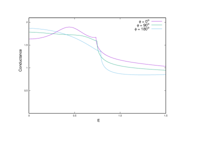
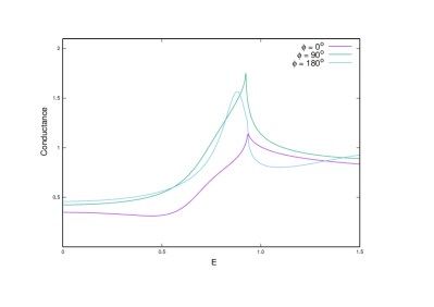
In Figs. 10 and 11 we show the angular dependence for . In the case in Fig. 10 we see that the angular dependence closely resembles the angular dependence in Fig. 8 for supplementary angles: that is, the conductance for and is similar to the conductance for and and vice versa. This corresponds to the periodicity, where the thickness difference between and represents half the period in the thickness dependence. Between the parallel () and antiparallel () configuration, the phase advances by .
We see a similar pattern in the angular dependence in the cases as well. The conductance for is the same as in Fig. 7 where at we see two peaks: one at low bias and one within the subgap region. For we see the two peaks shift to the right, with the higher peak moving into the critical bias. Finally at the conductance has merged into a single peak just below the critical bias. This is the same behavior as seen in Fig. 5, except that the periodicity in the thickness is . Indeed, the angle advances the phase of the overall oscillatory spin-split behavior by when going from a parallel to an antiparallel configuration. In the case, only for certain ranges of thicknesses would the valve effect be noticeable (when the peak was in the middle of the subgap region). We see now that in the structure, the peaks change in position with . This means the valve effect is apparent for any thickness, as any minimum found at will become a maximum when the magnetization is rotated by a certain angle . We also note that the barrier doubles the effective periodicity in the conductance subgap features, but the angular dependence between parallel and antiparallel advances the phase of the thickness by the equivalent wavelength in both cases.
In Sec. IV we summarize our results and how they may apply to real devices and experiments.
IV Conclusion
In this paper we have analyzed the quasiparticle conductance ferromagnetic Josephson structure using a numerical approach. Our analysis is in the ballistic limit, and it includes interfacial scattering characterized by delta-function barrier parameters. We have included a normal metal contact , with interfacial imperfections, which simplifies the calculation of the conductance via the BTK method. In the calculation of the pair amplitude we use a self consistent method that allows both superconductors to have an independent phase. We found that the total phase difference in equilibrium is either or .
To better understand the numerical results, we have used an analytic approximation for both the and systems. In this approximation, we assumed a one-dimensional multilayer with a constant pair potential . We also assume an imperfect normal metal contact (with interfacial scattering) for the system as well as interfacial scattering at the interface for the system. We found that for large thicknesses the conductance forms new peaks at the critical bias which we call the resonance peaks. In the case the peaks form at equally spaced intervals which we call the resonance thicknesses, with harmonic number . For higher ordered harmonics () there exists multiple peaks which are also evenly spaced between the zero bias and critical bias conductance. We determined in Sec. II.3 that these resonances are due to the interference of Andreev reflected particles at the interface with those reflected at the interface with non-zero scattering barriers. At higher harmonics () the conductance is oscillatory just above the critical bias and slowly decays at the same rate for all harmonics. The frequencies of these oscillations are approximately proportional to the harmonic number . In the case we found two resonance behaviors: “even” and “odd”. The even harmonic resonances are the same as those in the case for even values of , but the odd harmonics have an additional term that depends on the ratio of (see Eq. (II.3)). This term reduces the resonant thickness of the odd conductance peaks. The oscillatory conductance above the gap is also shifted by this thickness dependence in the odd harmonic thicknesses.
We then applied our analytic approximation to the ferromagnetic and systems. In Ref. spinsplitpaper, we studied the spin-split conductance of the system, where the conductance peak oscillates between the critical bias and near zero bias for varying thicknesses of the layer over a wavelength of . We did so for only small thicknesses of , just above the harmonic. In this paper, we studied the same effects on the harmonic, where there are two conductance peaks. Both peaks oscillate in position together between the subgap region and the zero bias conductance for the low bias peak, and the critical bias and subgap region for the higher bias peak. Between those two thickness values, each peak splits, resulting in multiple subgap peaks in the conductance. This also applies to the case. In our analysis of the Josephson structure, we saw that for even relatively small values of the layer thickness (less than the coherence length of the superconductor), the conductance displays multiple subgap peaks. This is because the spin-split oscillations can pull the higher order harmonic peaks into the subgap region since the first harmonic thickness () is reduced by the presence of the layer.
Armed with this qualitative understanding of the layer thickness dependence of our analytic calculation, we were then ready to consider the results for the fully self-consistent ferromagnetic Josephson structure. We studied the thickness dependence in the parallel configuration of the layer magnetizations () for the case of clean interfaces and imperfect interfaces. In some cases we assume a nonzero scattering barrier due to a normal metal contact , which we found to enhance the conductance peaks by decreasing the average subgap conductance. In our numerical calculations we found the same qualitative features of the subgap conductance as found in the analytic system. We carefully considered the barrier dependence of the conductance. We find that the inclusion of an scattering barrier allows for multiple subgap peaks. For example, by closely observing spin-split oscillation with in Fig. 7(a) we could see how a single subgap peak at becomes two subgap peaks at , with one peak being near the critical bias and one being at low bias. This is in contrast to the case or the superconducting spin valve where, for similar thicknesses of the layers, we only saw a single subgap conductance peak. We found that the inclusion of interfacial scattering does not greatly affect the conductance peak structure, but the barriers have a major impact on the subgap structure by forming dips in the subgap conductance. These dips do not have the same periodicity as the peak structure, which can lead to complex features in the subgap such as points of inflection.
We concluded this work with a study on the the angular dependence of the ferromagnetic Josephson structure. We calculated the conductance for multiple angles of the relative orientation of the ferromagnetic layer magnetizations (see Fig. 1) in the configuration. The angular dependence is similar to that on . By rotating between the parallel and antiparallel configuration, the phase of the spin-split conductance oscillations advances by in the case and by in the case. This is, in both cases, equivalent to increasing the thickness by . This is in stark contrast to the structure, where the angular dependence was found only in the subgap peak height and not in the position of the peaks within the subgap. This allows for a very large valve effect, on the order of the quantum of conductance per channel, which may prove useful in future spintronic devices.
Although we have learned about many new exciting features unique to the ferromagnetic Josephson structures, there are still many unanswered questions. For instance, we were unable to analytically determine the odd resonance thicknesses and had to settle for a phenomenological approximation. In addition, we have not determined how the angular dependence is related to the spin-split conductance oscillations. Many more questions that could be asked, such as the and layer thickness dependencies and even the study of the Josephson structure. We also assumed one imperfect contact, and have not studied the effect of two imperfect contacts. We believe that this paper, however, leaves a good foundation and highlights some of the more unique aspects worthy of future study. We hope that this work will be useful for future experiments into ferromagnetic Josephson structures and their application in spintronic devices.
Acknowledgements.
The authors thank I.N. Krivorotov (University of California, Irvine) for many illuminating discussions on the experimental issues. This work was supported in part by DOE grant No. DE-SC0014467References
- (1) E. Tsymbal and I. Žutić, Handbook on spin transport and magnetism, CRC Press, Boca Raton, Florida (2012).
- (2) M. Eschrig, Rep. Prog. Phys. 78, 104501 (2015).
- (3) A. F. Andreev, Sov. Phys. JETP 19, 1228 (1964).
- (4) V. L. Berezinskii, JETP Lett. 20, 287 (1975).
- (5) K. Halterman and O. T. Valls, Phys. Rev. B66, 224516 (2002).
- (6) R. S. Keizer, S. T. B. Goennenwein, T. M. Klapwijk, G. Miao, G. Xiao, and A. Gupta, Nature 439, 825 (2006).
- (7) A. A. Jara, C. Safranski, I. N. Krivorotov, C.-T. Wu. A. N. Malmi-Kakkada, O. T. Valls, and K. Halterman, Phys. Rev. B89, 184502 (2014).
- (8) N. Satchell and N. O. Birge, Phys. Rev. B97, 214509 (2018).
- (9) B. M. Niedzielski, T. J. Bertus, J. A. Glick, R. Loloee, W. P. Pratt, Jr., and N. O. Birge, Phys. Rev. B97, 024517 (2018).
- (10) C. Klose, T. S. Khaire, Y. Wang, W. P. Pratt, Jr., Norman O. Birge, B. J. McMorran, T. P. Ginley, J. A. Borchers, B. J. Kirby, B. B. Maranville, and J. Unguris, Phys. Rev. Lett. 108, 127002 (2012).
- (11) E. C. Gingrich, B. M. Niedzielski, J. A. Glick, Y. Wang, D. L. Miller, R. Loloee, W. P. Pratt Jr, N. O. Birge, Nature Physics 12, 564-567 (2016).
- (12) M. A. Silaev, I. V. Tokatly, and F. S. Bergeret, Phys. Rev. B95, 184508 (2017).
- (13) D.S. Holmes, A.L Ripple, and M.A. Manheimer, Trans. App.l Supercond. 23 170610 (2013).
- (14) T.I. Larkin et al. Appl. Phys. Lett. 100 222601 (2012).
- (15) M. A. Manheimer, IEEE Trans. Appl. Supercond. 25, 1301704 (2015).
- (16) D. S. Holmes, A. L. Ripple, M. A. Manheimer, IEEE Trans. Appl. Supercond. 23, 1701610 (2013).
- (17) V. V. Ryazanov, V. A. Oboznov, A. Yu. Rusanov, A. V. Veretennikov, A. A. Golubov, and J. Aarts Phys. Rev. Lett. 86, 2427 (2001).
- (18) T. Kontos, M. Aprili, J. Lesueur, F. Genêt, B. Stephanidis, and R. Boursier Phys. Rev. Lett. 89, 137007 (2002).
- (19) T. Yamishita, K. Tanikawa, and S. Maekawa, Phys. Rev. Lett. 95, 097001 (2005).
- (20) K. Halterman, O.T. Valls, and C-T Wu, Phys. Rev. B92, 174516 (2015).
- (21) K. Halterman and O. T. Valls Phys. Rev. B 69, 014517 (2004).
- (22) A. I. Buzdin, L. N. Bulaevskii, and S. V. Panyukov, Pisma Zh. Eksp. Teor. Fiz. 35, 147 (1982) [JETP Lett.35, 178 (1982)].
- (23) A. I. Buzdin and M. Y. Kuprianov, Pisma Zh. Eksp. Teor. Fiz. 53, 308 (1991) [JETP Lett.53, 321 (1991)].
- (24) C-T Wu, O.T. Valls and K. Halterman, Phys. Rev. B90, 054523, (2014).
- (25) E. Moen, O. T. Valls, Phys. Rev. B97, 174506 (2018).
- (26) E. Moen, O. T. Valls, Phys. Rev. B95, 054503 (2017).
- (27) E. Moen, O. T. Valls, Phys. Rev. B98 104512 (2018).
- (28) B. D. Josephson, Physics Letters 1 251 (1962).
- (29) C. Kittel, Introduction to Solid State Physics – 7th ed., (John Wiley and Sons, Inc., New York, NY, 1996).
- (30) P. W. Forder, J. Phys. D: Appl. Phys. 10 1413 (1997).
- (31) T. P. Orlando and K. A. Delin, Foundations of Applied Superconductivity pp. 393-488 (Addison-Wesley Publishing Company, Reading, MA, 1991).
- (32) G. Deutscher and P. G. de Gennes, Proximity Effects in Superconductivity, edited by R. D. Parks (Dekker, New York), pp. 1005-1034 (1969).
- (33) L. J. Barnes, Phys. Rev. 184, 434 (1969).
- (34) J. B. Hansen, M. T. Levinsen, P. E. Lindelof, B. Dueholm, J. Mygind, N. F. Pedersen, and O. H. Soerensen, Appl. Phys. Lett. 35, 28 (1979).
- (35) T. I. Baturina, D. R. Islamov, and Z. D. Kvon, Jetp Lett. 75 326 (2002).
- (36) F. Giubileo, M. Aprili, F. Bobba, S. Piano, A. Scarfato, A. M. Cucolo, Phys. Rev. B 72, 174518 (2005).
- (37) G. E. Blonder, M. Tinkham, and T. M. Klapwijk, Phys. Rev. B25, 4515 (1982).
- (38) M. Octavio, M. Tinkham, G. E. Blonder, and T. M. Klapwijk, Phys. Rev. B 27, 6739 (1983).
- (39) B. Lu, P. Burset, and Y. Tanaka, arXiv:1907.07370 (2019).
- (40) R. Kümmel, U. Gunsenheimer, and R. Nicolsky, Phys. Rev. B 42, 3992 (1990).
- (41) C. Cuevas, J. Hammer, J. Kopu, J. K. Viljas, and M. Eschrig, Phys. Rev. B 73 184505 (2006).
- (42) P. W. Anderson, J. Phys. Chem. Solids 11, 26 (1959).
- (43) A. A. Abrikosov, L. P. Gorkov and I. E. Dzyaloshinski, Methods of Quantum Field Theory in Statistical Physics (Dover, 1963).
- (44) K. D. Usadel, Phys. Rev. Lett. 25, 507 (1970).
- (45) Buzdin, A. I., and M. Y. Kuprianov, Pisima Zh. Eksp. Teor. Phys. 52, 1089-1091 [JETP Lett. 52, 487-491 (1990)].
- (46) F.S. Bergeret, A.F Volkov, and K.B. Efetov, Rev. Mod. Phys. 77, 1321 (2005).
- (47) M. Eschrig and T. Löfwander, Nature physics 4, 138 (2008).
- (48) P. V. Leksin, N. N. Garif’yanov, I. A. Garifullin, Ya. V. Fominov, J. Schumann, Y. Krupskaya, V. Kataev, O. G. Schmidt, and B. Büchner, Phys. Rev. Lett. 109, 057005 (2012).
- (49) F. S. Bergeret, A. F. Volkov, and K. B. Efetov, Appl. Phys. A 89, 599 (2007).
- (50) Y. Kalcheim, O. Millo, A. DiBernardo, A. Pal and J.W. Robinson, Phys. Rev. B92, 060501 (2015).
- (51) A. Singh, S. Voltan, K. Lahabi, and J. Aarts, Phys. Rev. X 5, 021019 (2015).
- (52) K.Halterman and M. Alidoust, arXiv:1607.03899 (2016).
- (53) P.F. Bagwell, Phys. Rev. B49, 6841 (1993).
- (54) F. Sols and J. Ferrer, Phys. Rev. B49, 15913 (1994).
- (55) J. Sanchez-Canizares and F. Sols, Phys. Rev. B55, 531 (1997).
- (56) G. Baym and L.P. Kadanoff, Phys. Rev. 124, 287 (1961).
- (57) A. Furusaki, Superlattices and Microstructures, Vol. 25, 809 (1999).
- (58) J. Bardeen, L. N. Cooper, and J. R. Schrieffer, Phys. Rev. 108, 1175 (1957).