Interaction-induced crossover between weak anti-localization and weak localization in a disordered InAs/GaSb double quantum well
Abstract
We present magneto-transport study in an InAs/GaSb double quantum well structure in the weak localization regime. As the charge carriers are depleted using a top gate electrode, we observe a crossover from weak anti-localization (WAL) to weak localization (WL), when the inelastic phase breaking time decreases below spin-orbit characteristic time as a result of enhanced electron-electron interactions at lower carrier concentrations. The same crossover is observed with increasing temperature. The linear temperature behavior of inelastic scattering rate indicates that the dominant phase breaking mechanism in our 2D system is due to electron-electron interaction.
InAs/GaSb heterostructures have recently been revisited by condensed matter physicists in quest for observing a topological phase of matter namely the quantum spin Hall insulator(QSHI) Liu et al. (2008); Knez et al. (2011, 2012); Suzuki et al. (2013); Knez et al. (2014a); Nichele et al. (2014); Knez et al. (2014b); Spanton et al. (2014); Du et al. (2015); Qu et al. (2015); Pribiag et al. (2015); Li et al. (2015); Karalic et al. (2016); Nichele et al. (2016); Nguyen et al. (2016); Yu et al. (2018); Shojaei et al. (2018); Krishtopenko et al. (2018); Wu et al. (2019); Karalic et al. (2019); Xiao et al. (2019); Sazgari et al. (2019). Topological insulators inherently possess strong spin-orbit coupling (SOC) together with band inversion Hasan and Kane (2010); Qi and Zhang (2011). Strong spin-orbit coupling embodied in InAs/GaSb bilayer QW system has been comprehensively studied both experimentally and theoretically. SOC in crystal structures stems from inversion asymmetry in the crystal potential which builds up an internal electric field. Analogous to the electric field of nuclei, the crystal field generates an effective magnetic field in the rest frame of the moving electrons, which in turn couples the spin and momentum of the electron Winkler (2003); Fabian et al. (2007). This coupling can be in the form of Dresselhaus interaction caused by a bulk inversion asymmetry Dresselhaus (1955), e.g. in zinc blende structures, or Rashba spin-orbit contribution due to structural inversion asymmetry of the confinement potential J. Ohkawa and Uemura (1974); Bychkov and Rashba (1984); Schierholz (2005); Ström et al. (2010); Crépin et al. (2012); Geissler et al. (2014); Manchon et al. (2015). The spin-orbit interaction lifts the spin degeneracy at even a zero magnetic field and provides a versatile tool to manipulate the electron spin without an external magnetic field, which is desired for spintronic applications and quantum information technology Žutić et al. (2004); Qi and Zhang (2011); Fiederling et al. (1999). For example, classical spin Hall effect and its inverse driven by SOC are useful tools for injection and detection of the spin in spintronics Brüne et al. (2012).
The effect of spin-orbit interaction has been widely studied in several low dimensional systems including two-dimensional electron gases (2DEGs) Jusserand et al. (1995); Qiu et al. (2004); Tikhonenko et al. (2008); Studer et al. (2009); Wang et al. (2018), QW heterostructures Luo et al. (1990); Nitta et al. (1997); Engels et al. (1997); Heida et al. (1998); Hu et al. (1999); Brosig et al. (1999); Papadakis et al. (1999); Grundler (2000); Koga et al. (2002); Shojaei et al. (2016); Beukman et al. (2017); Herzog et al. (2017); Nichele et al. (2017); Herling et al. (2017), topological insulators Assaf et al. (2013); Meng et al. (2018), etc. A strong SOC can be reflected in magnetoresistance measurements in two different ways. In high mobility systems a beating pattern in SdH oscillations may be observed as a result of two different SdH frequencies corresponding to carrier densities of each spin orientation split by SOC Grundler (2000); Shojaei et al. (2016); Beukman et al. (2017); Herzog et al. (2017); Nichele et al. (2017). On the other hand, in disordered low mobility structures, the strength of spin-orbit interaction can be quantified by the spin relaxation length () obtained from the low field magnetoresistance measurements where the strong SOC appears as a weak anti-localization phenomenon Herling et al. (2017); Meng et al. (2018).
In weakly disordered electronic systems, various scattering mechanisms in competition with each other determine the transport behavior of mesoscopic devices Hikami et al. (1980); Iordanskii et al. (1994); Niimi et al. (2010). Corresponding scattering rates or equivalently characteristic lengths, including the spin relaxation length , can be extracted from low-field magnetotransport study of the longitudinal conductivity. In a spin-degenerate system, the quantum interference of the electrons moving on time-reversed closed paths is constructive and gives rise to a negative correction to conductivity This phenomenon is called weak localization (WL) and a small magnetic field can suppress the the excess resistance due to this quantum interference. Nevertheless, in presence of SOC, the quantum correction to the zero-field conductivity becomes positive which is manifested by a decreased conductivity upon application of a small magnetic field known as the weak anti-localization (WAL) effect.
In this work, we report a gate-tunable and temperature-induced crossover from WAL to WL. Inelastic scattering rate due to electron-electron interactions is enhanced at low electron densities and leads to reduction of the dephasing length, . By applying a top gate voltage, we were able to tune the electron density and consequently the electron dephasing length to go below the SOC length. The enhancement of the inelastic scattering at lower densities implies that electron-electron interactions are the dominant inelastic scattering mechanism. However, the spin relaxation, and elastic scattering, lengths remain independent of . The WAL-WL crossover is observed also in the magnetoconductance plots as the temperature is varied; at elevated temperatures decreases below transitioning from WAL regime at low temperatures to WL regime at high temperatures.
The heterostructure used in the experiments was grown on a GaAs substrate by molecular beam epitaxy. Following an AlSb buffer layer of 1 thickness, the bilayer QW structure consisting of a 12.5 nm InAs layer on a 10 nm GaSb layer confined between two 50 nm thick AlGaSb barriers was grown. The top barrier was protected from oxidization by a 3 nm GaSb cap layer. A 205 m () Hall bar device was used in the measurements. The device mesa was formed by standard electron beam lithography followed by chemical wet etching. The etched surfaces were passivated by a 200 nm thick PECVD-grown Si3Ni4 layer which also served as the dielectric layer separating the top gate electrodes (Ti/Au) from the heterostructure. The ohmic contacts were made by Ge/Au/Ni metalization without annealing. Transport measurements were performed in a dilution refrigerator with base temperature of 10 mK using standard lock-in techniques with 10 nA current excitation at 7 Hz unless otherwise stated.
Similar to the heterostructure we used in our recent report on the localization of trivial edge states Sazgari et al. (2019), the structure in this study is also disordered by single layer of silicon atoms, however, in different position along the growth direction. In Ref. Sazgari et al. (2019), Si atoms were deposited inside the InAs at 2 atomic layer distance from the InAs/GaSb interface, while in the heterostructure of this work, the silicon atoms were placed at 1 atomic layer distance into the InAs layer with an average density of cm-2. Difference in the delta doping location resulted in a remarkable change in the transport properties which is possibly due to impurity-induced interfacial effects. In our previous study, the bilayer InAs/GaSb heterostructure exhibited a trivial insulator behavior with a sizable gap using dual gate electrodes. However, in the present work, the bilayer QW shows a semi-metallic behavior within the whole range of top and bottom gate voltages Sup .
The hallmark of the present study is the observation of a crossover between WAL and WL regimes in the magneto-resistance measurements that can be induced either by the top gate voltage or temperature. The magnetotransport measurements are well described by Hikami– Larkin– Nagaoka (HLN) interference model Hikami et al. (1980) which characterizes the WL and WAL phenomena in disordered two dimensional electronic systems by different scattering mechanisms and their corresponding length scales. According to HLN model, the quantum interference correction to the low field magnetoconductivity is given by Hikami et al. (1980); Iordanskii et al. (1994):
| (1) |
where is the digamma function and ’s are the characteristic magnetic fields each corresponds to a different scattering mechanism. By fitting the above equation to the magnetoconductance data we obtained the characteristic fields for inelastic dephasing , spin-orbit and elastic scatterings. One can then obtain the corresponding scattering length via the relation .
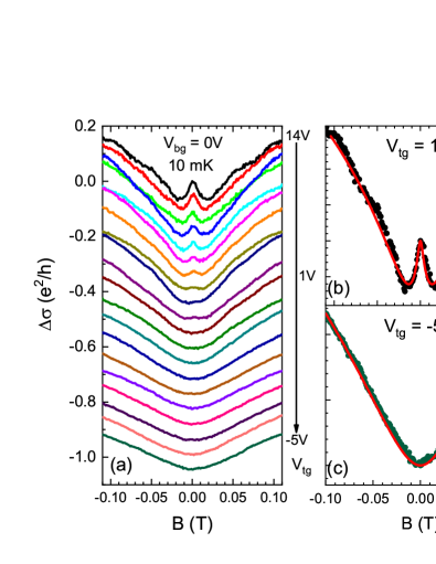
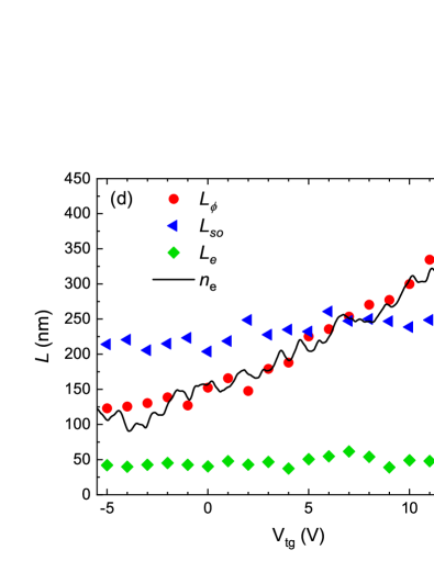
By application of the top gate voltage, a continuous change from WAL to WL regime is observed in the magnetotransport measurements. Figure 1 illustrates the change of the magneto-conductivity for different top gate voltages from +14 V to -5 V with 1 V steps. While at higher gate voltages the device represents a WAL feature, it gradually transforms into WL regime as the inelastic dephasing length declines by lowering the top gate voltage and finally crosses over the spin-orbit scattering length at where the WAL cusp diminishes and the sample acquires a WL feature (Fig. 1(a). The most pronounced WAL and WL characteristics at extreme gate voltages are illustrated in Fig. 1b and 1c, respectively, with perfect fits to the HLN equation. The scattering lengths calculated from each magnetoconductance curve are plotted as functions of top gate voltage in Fig. 1d. The elastic scattering length and the spin-orbit length are nearly independent of gate voltage, however, it can be seen that the inelastic dephasing length is strongly gate-dependent and decreases by decreasing the gate voltage. To demonstrate the correlation between and the carrier density , we plotted the electron density versus top gate voltage in the same graph. It is visible that the dephasing length due to inelastic scattering is linked to the carrier density suggesting that the dominant inelastic process is induced by the electron-electron interactions. It can also be seen in Fig. 1(d) that the density modulation in response to the top gate electric field is slightly nonlinear. This is attributed to surface trap states common to the III-V semiconductor interfaces Sazgari et al. (2019); Suzuki et al. (2011); Shibata et al. (2019) or impurity-induced charge states inside the bilayer QW.
This may explain the gate-independent spin relaxation length which is otherwise expected to change with the external electric field via the Rashba spin-orbit interaction Luo et al. (1990); Jusserand et al. (1995); Nitta et al. (1997); Engels et al. (1997); Heida et al. (1998); Hu et al. (1999); Brosig et al. (1999); Papadakis et al. (1999); Grundler (2000); Shojaei et al. (2016); Beukman et al. (2017); Herling et al. (2017). In other words, the out of plane electric field in the conducting channel is dominated by the crystal fields rather than the external gate-induced field. However, for 2D electron systems, the reported strengths of the Rashba effect are markedly different Luo et al. (1990); Jusserand et al. (1995); Nitta et al. (1997); Engels et al. (1997); Heida et al. (1998); Hu et al. (1999); Brosig et al. (1999); Papadakis et al. (1999); Grundler (2000). There is a puzzling discrepancy between theoretical expectations and experimental observations of the effect of external electric field on the Rashba SOI such that it is sometimes very weak or even absent Brosig et al. (1999) and in some experiments far stronger than what theory predicts Papadakis et al. (1999); Grundler (2000). For instance in Ref. Papadakis et al. (1999), a weak perpendicular electric field (2 orders of magnitude smaller than the typical built-in electric field) applied to the plane of a 2D hole gas was able to change the Rashba SOI by , whereas in reference to Grundler (2000), the Rashba coupling was enhanced by two folds when the field was changed only by within the range of applied gate voltage. Therefore, the exact effect of gate-induced electric field on the Rashba SOI has remained ambiguous. Above all, a precise investigation of Rashba effect incorporates the variation of electric field at constant carrier densities because otherwise the effects of density modulation and electric field variation on the amount of Rashba SOI can not be separated.
On the other hand, we observe the electron dephasing length to be a function of carrier concentration. At low temperatures in disordered electronic systems, the phase breaking length is determined by electron-electron collisions in the form of direct Coulomb interaction between conducting electrons or inelastic scattering by the electromagnetic field fluctuations in the potential landscape generated by the moving electrons. The e-e inelastic scattering is sensitive to the carrier concentration as it changes the potential landscape for cruising electrons. At low temperatures, the scattering rate corresponding to the e-e collisions with small energy transfer, often referred to as Nyquist scattering, is given by Altshuler et al. (1982); Taboryski and Lindelof (1990):
| (2) |
where, is the Fermi energy, is the electron effective mass, and is the transport time also called mean free time i.e. the time between consecutive scattering events. And is the dimensionless conductivity in units of . The characteristic scattering lengths are related to their corresponding times via , where is the electron diffusion coefficient given by:
| (3) |
Referring to Eq. 2, at a given temperature, the Nyquist time thus the dephasing length decreases at lower charge densities (or equivalently smaller ) consistent with our observation of gate-dependent dephasing length. As illustrated in Fig. 1(d), we observe that reduces monotonically with decreasing electron concentration at lower top gate voltages in agreement with the Nyquist interaction model. Therefore, in the heterostructure of this study, the phase breaking time is determined by the characteristic time of the electron scattering by electromagnetic fluctuations with small energy transfer that is the Nyquist time ().
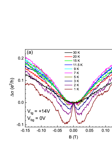
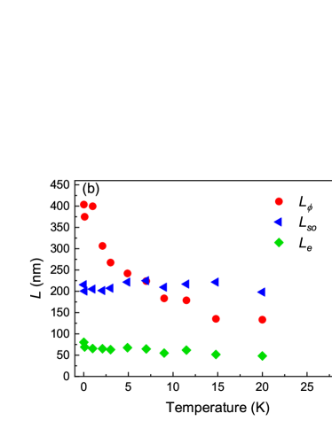
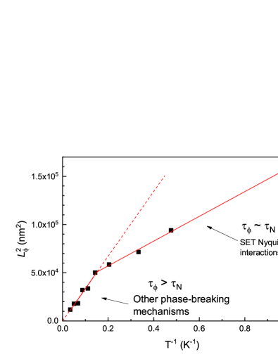
Theory predicts that inelastic scattering rates magnify at higher temperatures. The temperature dependence of the quantum interference corrections due to electron scatterings is quantified by the time during which the electron wavefunction remains phase-coherent. In highly interacting two-dimensional electron systems, the phase breaking scattering mechanisms are dominated by Nyquist scattering rate induced by electron-electron interaction given by Eq. 2. We conducted the temperature study of the magnetoconductance at where a prominent WAL behavior is observed at lowest temperatures which indicates that the elastic and spin-orbit scatterings are dominant over inelastic phase breaking interactions. As expected, the inelastic scattering mechanisms strengthen at increased temperatures leading to a transition from WAL to WL regime when the reduces below the . The temperature study of the magnetoconductance correction is indicated in Fig. 2. The positive cusp of the conductance correction around zero field, that characterizes the WAL, gradually suppresses by increasing the temperature until it enters the WL regime at K where the crossover occurs (Fig. 2a). The extracted characteristic lengths which quantifies the crossover are shown in Fig. 2b where and are insensitive to temperature. Consistent with Eq. 2, , which is here equivalent to , decreases with rising temperature. As illustrated in Fig. 3, the square of the dephasing length () is linearly proportional to the inverse temperature. However, the slopes in the WL and WAL regimes are different. At sufficiently low temperatures ( K), where the WAL effect is dominant, the slope of the fit line is m2K. On the other hand, substituting all the numbers (assuming the effective mass as Beukman et al. (2017)) in equation 2, which is valid for low temperatures, we obtain a slope of m2K which is in perfect agreement with the line slope for WAL (low temperature) regime in Fig. 3. At higher temperatures, however, in the WL regime, the slope at which the dephasing length (the Nyquist scattering rate) decreases (increases) with temperature is higher (lower) than that for low temperature regime. The slope of the fit line for K is m2K more than two fold larger than that for lower temperatures. At elevated temperatures, the inelastic dephasing mechanisms may deviate from small energy transfer Nyquist interactions due to thermal excitations when the larger energy transfer collisions may play the dominant role. Indeed the phase breaking electron-electron interactions reduces at higher temperatures and the inelastic dephasing rate is decreased by the logarithmic factor in Eq. 2 Altshuler et al. (1982).
In conclusion, we observed an interaction-induced crossover between the WAL and WL phenomena in our intentionally disordered InAs/GaSb bilayer QW structure driven by top gate voltage and temperature. The heterostructure with Si delta-doped atoms near the interface of electron and hole QWs demonstrates WAL feature in magnetoconductance measurements at high carrier densities at lowest temperatures as an evidence for strong SOI. Using the theoretical HLN model, we obtained the gate and temperature dependences of the characteristic scattering lengths corresponding to three different scattering mechanisms. The elastic scattering length is found as nm which is consistent with the mean spacing between Si dopants of nm. It is almost independent of gate voltage and temperature, which indicates the short range scattering induced by impurity or interface roughness is dominant. The SO scattering length also shows no dependence on temperature and gate voltage. We believe that the effective gate-induced electric field is reduced by impurity and trap states leading to a gate-independent . The only parameter responsible for the temperature and gate-driven crossover is the electron dephasing length which changes the magnetotransport behavior when it crosses over with an indication of enhanced interactions at lower temperatures and charge concentrations. The temperature and gate dependent analysis of the inelastic phase breaking length indicates that the Nyquist scattering, characterized by electron-electron interactions with SET, is the dominant dephasing mechanism at low temperatures where the spin-orbit scattering is still governing the magneto-conductance behavior with a WAL feature. At higher temperatures the inealastic scattering takes over the SO interaction thus leading to the WL effect. At the same time, the dephasing time increases above the Nyquist time meaning that the Nyquist interactions suppressed at higher temperatures and other inelastic processes perhaps with larger energy transfer becomes important.
References
- Liu et al. (2008) C. Liu, T. L. Hughes, X.-L. Qi, K. Wang, and S.-C. Zhang, Phys. Rev. Lett. 100, 236601 (2008).
- Knez et al. (2011) I. Knez, R.-R. Du, and G. Sullivan, Phys. Rev. Lett. 107, 136603 (2011).
- Knez et al. (2012) I. Knez, R.-R. Du, and G. Sullivan, Phys. Rev. Lett. 109, 186603 (2012).
- Suzuki et al. (2013) K. Suzuki, Y. Harada, K. Onomitsu, and K. Muraki, Phys. Rev. B 87, 235311 (2013).
- Knez et al. (2014a) I. Knez, C. T. Rettner, S.-H. Yang, S. S. P. Parkin, L. Du, R.-R. Du, and G. Sullivan, Phys. Rev. Lett. 112, 026602 (2014a).
- Nichele et al. (2014) F. Nichele, A. N. Pal, P. Pietsch, T. Ihn, K. Ensslin, C. Charpentier, and W. Wegscheider, Phys. Rev. Lett. 112, 036802 (2014).
- Knez et al. (2014b) I. Knez, C. T. Rettner, S.-H. Yang, S. S. P. Parkin, L. Du, R.-R. Du, and G. Sullivan, Phys. Rev. Lett. 112, 026602 (2014b).
- Spanton et al. (2014) E. M. Spanton, K. C. Nowack, L. Du, G. Sullivan, R.-R. Du, and K. A. Moler, Phys. Rev. Lett. 113, 026804 (2014).
- Du et al. (2015) L. Du, I. Knez, G. Sullivan, and R.-R. Du, Phys. Rev. Lett. 114, 096802 (2015).
- Qu et al. (2015) F. Qu, A. J. A. Beukman, S. Nadj-Perge, M. Wimmer, B.-M. Nguyen, W. Yi, J. Thorp, M. Sokolich, A. A. Kiselev, M. J. Manfra, C. M. Marcus, and L. P. Kouwenhoven, Phys. Rev. Lett. 115, 036803 (2015).
- Pribiag et al. (2015) V. S. Pribiag, A. J. A. Beukman, F. Qu, M. C. Cassidy, C. Charpentier, W. Wegscheider, and L. P. Kouwenhoven, Nature Nanotechnology 10, 593 (2015).
- Li et al. (2015) T. Li, P. Wang, H. Fu, L. Du, K. A. Schreiber, X. Mu, X. Liu, G. Sullivan, G. A. Csáthy, X. Lin, and R.-R. Du, Phys. Rev. Lett. 115, 136804 (2015).
- Karalic et al. (2016) M. Karalic, S. Mueller, C. Mittag, K. Pakrouski, Q. Wu, A. A. Soluyanov, M. Troyer, T. Tschirky, W. Wegscheider, K. Ensslin, and T. Ihn, Phys. Rev. B 94, 241402 (2016).
- Nichele et al. (2016) F. Nichele, H. J. Suominen, M. Kjaergaard, C. M. Marcus, E. Sajadi, J. A. Folk, F. Qu, A. J. A. Beukman, F. K. de Vries, J. van Veen, S. Nadj-Perge, L. P. Kouwenhoven, B.-M. Nguyen, A. A. Kiselev, W. Yi, M. Sokolich, M. J. Manfra, E. M. Spanton, and K. A. Moler, New Journal of Physics 18, 083005 (2016).
- Nguyen et al. (2016) B.-M. Nguyen, A. A. Kiselev, R. Noah, W. Yi, F. Qu, A. J. A. Beukman, F. K. de Vries, J. van Veen, S. Nadj-Perge, L. P. Kouwenhoven, M. Kjaergaard, H. J. Suominen, F. Nichele, C. M. Marcus, M. J. Manfra, and M. Sokolich, Phys. Rev. Lett. 117, 077701 (2016).
- Yu et al. (2018) W. Yu, V. Clericò, C. H. Fuentevilla, X. Shi, Y. Jiang, D. Saha, W. K. Lou, K. Chang, D. H. Huang, G. Gumbs, D. Smirnov, C. J. Stanton, Z. Jiang, V. Bellani, Y. Meziani, E. Diez, W. Pan, S. D. Hawkins, and J. F. Klem, New Journal of Physics 20, 053062 (2018).
- Shojaei et al. (2018) B. Shojaei, A. P. McFadden, M. Pendharkar, J. S. Lee, M. E. Flatté, and C. J. Palmstrøm, Phys. Rev. Materials 2, 064603 (2018).
- Krishtopenko et al. (2018) S. S. Krishtopenko, S. Ruffenach, F. Gonzalez-Posada, G. Boissier, M. Marcinkiewicz, M. A. Fadeev, A. M. Kadykov, V. V. Rumyantsev, S. V. Morozov, V. I. Gavrilenko, C. Consejo, W. Desrat, B. Jouault, W. Knap, E. Tournié, and F. Teppe, Phys. Rev. B 97, 245419 (2018).
- Wu et al. (2019) X. Wu, W. Lou, K. Chang, G. Sullivan, and R.-R. Du, Phys. Rev. B 99, 085307 (2019).
- Karalic et al. (2019) M. Karalic, C. Mittag, S. Mueller, T. Tschirky, W. Wegscheider, K. Ensslin, T. Ihn, and L. Glazman, Phys. Rev. B 99, 201402 (2019).
- Xiao et al. (2019) D. Xiao, C.-X. Liu, N. Samarth, and L.-H. Hu, Phys. Rev. Lett. 122, 186802 (2019).
- Sazgari et al. (2019) V. Sazgari, G. Sullivan, and I. I. Kaya, Phys. Rev. B 100, 041404 (2019).
- Hasan and Kane (2010) M. Z. Hasan and C. L. Kane, Rev. Mod. Phys. 82, 3045 (2010).
- Qi and Zhang (2011) X.-L. Qi and S.-C. Zhang, Rev. Mod. Phys. 83, 1057 (2011).
- Winkler (2003) R. Winkler, Springer Tracts in Modern Physics 191, 1 (2003).
- Fabian et al. (2007) J. Fabian, A. Matos-Abiague, C. Ertler, P. Stano, and I. Žutić, Acta Physica Slovaca. Reviews and Tutorials 57, 565 (2007).
- Dresselhaus (1955) G. Dresselhaus, Physical Review 100, 580 (1955).
- J. Ohkawa and Uemura (1974) F. J. Ohkawa and Y. Uemura, Journal of the Physical Society of Japan 37, 1325 (1974).
- Bychkov and Rashba (1984) Y. A. Bychkov and E. I. Rashba, Journal of physics C: Solid state physics 17, 6039 (1984).
- Schierholz (2005) C. Schierholz, Rashba Spin-Orbit Interaction in Low and High Magnetic Fields (Cuvillier Verlag, 2005).
- Ström et al. (2010) A. Ström, H. Johannesson, and G. I. Japaridze, Phys. Rev. Lett. 104, 256804 (2010).
- Crépin et al. (2012) F. m. c. Crépin, J. C. Budich, F. Dolcini, P. Recher, and B. Trauzettel, Phys. Rev. B 86, 121106 (2012).
- Geissler et al. (2014) F. Geissler, F. m. c. Crépin, and B. Trauzettel, Phys. Rev. B 89, 235136 (2014).
- Manchon et al. (2015) A. Manchon, H. C. Koo, J. Nitta, S. M. Frolov, and R. A. Duine, Nature materials 14 9, 871 (2015).
- Žutić et al. (2004) I. Žutić, J. Fabian, and S. Das Sarma, Rev. Mod. Phys. 76, 323 (2004).
- Fiederling et al. (1999) R. Fiederling, M. Keim, G. Reuscher, W. Ossau, G. Schmidt, A. Waag, and L. W. Molenkamp, Nature 402, 787 (1999).
- Brüne et al. (2012) C. Brüne, A. Roth, H. Buhmann, E. M. Hankiewicz, L. W. Molenkamp, J. Maciejko, X.-L. Qi, and S.-C. Zhang, Nature Physics 8, 485 EP (2012), article.
- Jusserand et al. (1995) B. Jusserand, D. Richards, G. Allan, C. Priester, and B. Etienne, Physical Review B 51, 4707 (1995).
- Qiu et al. (2004) Z. J. Qiu, Y. S. Gui, T. Lin, N. Dai, J. H. Chu, N. Tang, J. Lu, and B. Shen, Phys. Rev. B 69, 125335 (2004).
- Tikhonenko et al. (2008) F. V. Tikhonenko, D. W. Horsell, R. V. Gorbachev, and A. K. Savchenko, Phys. Rev. Lett. 100, 056802 (2008).
- Studer et al. (2009) M. Studer, G. Salis, K. Ensslin, D. C. Driscoll, and A. C. Gossard, Phys. Rev. Lett. 103, 027201 (2009).
- Wang et al. (2018) L. Wang, M. Yin, A. Khan, S. Muhtadi, F. Asif, E. S. Choi, and T. Datta, Phys. Rev. Applied 9, 024006 (2018).
- Luo et al. (1990) J. Luo, H. Munekata, F. F. Fang, and P. J. Stiles, Phys. Rev. B 41, 7685 (1990).
- Nitta et al. (1997) J. Nitta, T. Akazaki, H. Takayanagi, and T. Enoki, Physical Review Letters 78, 1335 (1997).
- Engels et al. (1997) G. Engels, J. Lange, T. Schäpers, and H. Lüth, Phys. Rev. B 55, R1958 (1997).
- Heida et al. (1998) J. Heida, B. Van Wees, J. Kuipers, T. Klapwijk, and G. Borghs, Physical Review B 57, 11911 (1998).
- Hu et al. (1999) C.-M. Hu, J. Nitta, T. Akazaki, H. Takayanagi, J. Osaka, P. Pfeffer, and W. Zawadzki, Physical Review B 60, 7736 (1999).
- Brosig et al. (1999) S. Brosig, K. Ensslin, R. Warburton, C. Nguyen, B. Brar, M. Thomas, and H. Kroemer, Physical Review B 60, R13989 (1999).
- Papadakis et al. (1999) S. Papadakis, E. De Poortere, H. Manoharan, M. Shayegan, and R. Winkler, Science 283, 2056 (1999).
- Grundler (2000) D. Grundler, Phys. Rev. Lett. 84, 6074 (2000).
- Koga et al. (2002) T. Koga, J. Nitta, T. Akazaki, and H. Takayanagi, Phys. Rev. Lett. 89, 046801 (2002).
- Shojaei et al. (2016) B. Shojaei, P. O’Malley, J. Shabani, P. Roushan, B. Schultz, R. Lutchyn, C. Nayak, J. Martinis, and C. Palmstrøm, Physical Review B 93, 075302 (2016).
- Beukman et al. (2017) A. J. A. Beukman, F. K. de Vries, J. van Veen, R. Skolasinski, M. Wimmer, F. Qu, D. T. de Vries, B.-M. Nguyen, W. Yi, A. A. Kiselev, M. Sokolich, M. J. Manfra, F. Nichele, C. M. Marcus, and L. P. Kouwenhoven, Phys. Rev. B 96, 241401 (2017).
- Herzog et al. (2017) F. Herzog, H. Hardtdegen, T. Schäpers, D. Grundler, and M. Wilde, New Journal of Physics 19, 103012 (2017).
- Nichele et al. (2017) F. Nichele, M. Kjaergaard, H. J. Suominen, R. Skolasinski, M. Wimmer, B.-M. Nguyen, A. A. Kiselev, W. Yi, M. Sokolich, M. J. Manfra, F. Qu, A. J. A. Beukman, L. P. Kouwenhoven, and C. M. Marcus, Phys. Rev. Lett. 118, 016801 (2017).
- Herling et al. (2017) F. Herling, C. Morrison, C. S. Knox, S. Zhang, O. Newell, M. Myronov, E. H. Linfield, and C. H. Marrows, Phys. Rev. B 95, 155307 (2017).
- Assaf et al. (2013) B. A. Assaf, T. Cardinal, P. Wei, F. Katmis, J. S. Moodera, and D. Heiman, Applied Physics Letters 102, 012102 (2013), https://doi.org/10.1063/1.4773207 .
- Meng et al. (2018) M. Meng, S. Huang, C. Tan, J. Wu, Y. Jing, H. Peng, and H. Q. Xu, Nanoscale 10, 2704 (2018).
- Hikami et al. (1980) S. Hikami, A. I. Larkin, and Y. Nagaoka, Progress of Theoretical Physics 63, 707 (1980), http://oup.prod.sis.lan/ptp/article-pdf/63/2/707/5336056/63-2-707.pdf .
- Iordanskii et al. (1994) S. Iordanskii, Y. B. Lyanda-Geller, and G. Pikus, ZhETF Pisma Redaktsiiu 60, 199 (1994).
- Niimi et al. (2010) Y. Niimi, Y. Baines, T. Capron, D. Mailly, F.-Y. Lo, A. D. Wieck, T. Meunier, L. Saminadayar, and C. Bäuerle, Phys. Rev. B 81, 245306 (2010).
- (62) “See supplemental material for detailed chacteristics of the wafer heterostructure,” .
- Suzuki et al. (2011) K. Suzuki, Y. Harada, F. Maeda, K. Onomitsu, T. Yamaguchi, and K. Muraki, Applied Physics Express 4, 125702 (2011).
- Shibata et al. (2019) K. Shibata, M. Karalic, C. Mittag, T. Tschirky, C. Reichl, H. Ito, K. Hashimoto, T. Tomimatsu, Y. Hirayama, W. Wegscheider, T. Ihn, and K. Ensslin, Applied Physics Letters 114, 232102 (2019).
- Altshuler et al. (1982) B. L. Altshuler, A. G. Aronov, and D. E. Khmelnitsky, Journal of Physics C: Solid State Physics 15, 7367 (1982).
- Taboryski and Lindelof (1990) R. Taboryski and P. E. Lindelof, Semiconductor Science and Technology 5, 933 (1990).