OFDM-Based Optical Spatial Modulation
Abstract
SM has proven to be a promising multiple-input-multiple-output (MIMO) technique which provides high energy efficiency and reduces system complexity. In SM, only one transmitter is active at any given time while the rest of them remain silent. The index of the active transmitter carries information. This spatial information is in addition to the data carried by the constellation symbols in the signal domain. Therefore, SM increases the transmission rate of the communication system compared to single-input-single-output and space-time block coding (STBC)-MIMO. For signal domain data encoding, OFDM has been widely adopted. The key benefits in multi-carrier intensity-modulation and direct-detection (IM/DD) systems are: i) the capability to achieve high spectral efficiency and ii) the ability to effectively mitigate direct-current (DC) wander effects and the impact of ambient light. However, current off-the-shelf light emitting diodes (LEDs) which are used as transmit entities are primarily bandwidth limited. Thus, there are benefits of combining SM and OFDM to enhance transmission speeds while maintaining low complexity. In this paper, the two most common OFDM-based SM types, namely frequency domain SM (FD-SM) and time domain SM (TD-SM), are investigated for optical wireless communications (OWC). Moreover, proof-of-concept experimental results are presented to showcase practical feasibility of both techniques. The obtained results are also compared with Monte Carlo simulations. The results show that TD-SM with an optimal maximum-a-posteriori-probability (MAP) detector significantly outperforms FD-SM. It can be inferred from the results that TD-SM is a strong candidate among OFDM-based optical SM systems for future optical IM/DD wireless communication systems.
Index Terms:
Spatial modulation (SM), Orthogonal frequency division multiplexing (OFDM), Light fidelity (LiFi), Optical wireless communications (OWC)I Introduction
Advanced capabilities of mobile devices such as virtual/augmented reality (VR/AR), high definition video/audio streaming, low-latency gaming and internet-of-things (IoT) create a data-greedy ecosystem. The recent forecasts show that the global mobile data traffic will reach 49 exabytes ( bytes) by 2021[1]. It is also reported in [2] that if the mobile data demand keeps increasing at the same rate as that of the last 10 years, the radio frequency (RF) spectrum will be completely saturated by 2035. Thus, the higher frequency portion of the spectrum is starting to be considered as a viable solution for the potential congestion. Similar to this trend, optical wireless communications (OWC) offers the utilization of the optical portion of the electromagnetic spectrum e.g., visible light (VL), infra-red (IR) and ultra-violet (UV) to create a wireless broadband medium between the ends. Similarly, the light-fidelity (LiFi) which uses VL in the downlink and IR in the uplink forms a bi-directional optical attocellular network that supports multi-user connectivity and seamless handover[3]. In LiFi, ordinary off-the-shelf light emitting diodes (LEDs) and photo-diodes (PDs) will serve as the transmit and receive units, respectively. As the VL and IR rays are naturally blocked by opaque walls, LiFi could achieve very high area spectral efficiency due to significantly reduced co-channel interference in dense network deployments. Moreover, similar features help enhance security and reduce latency in LiFi [4, 5]. The information is carried by fluctuations in light intensity which is detected by the front-end optics and decoded at the receiver (RX). This incoherent transmission technique is referred to as intensity modulation and direct detection (IM/DD). Since the optical power of the LEDs are intrinsically limited to be real and positive valued, the information bearing signal is also limited by the same fundamental constraints. Furthermore, eye safety and linearity considerations as well as the dynamic range of the front-end opto-electronic elements bring additional limitations to the transmitted signal. Therefore, techniques developed and optimized for RF systems cannot be applied straightforwardly to IM/DD systems without significant changes.
The limited electrical bandwidth of the optical elements motivates the use of spatial multiplexing (SMX) [6, 7, 8, 9, 10, 11, 12] in OWC systems. For a LED and PD multiple-input-multiple-output (MIMO)-OWC system, the data rate could be enhanced -fold by harnessing SMX. However, the inter-channel interference (ICI) caused by channel coupling and detection complexity at the RX side are the major drawbacks of SMX. Spatial modulation (SM) is an alternative MIMO technique which avoids ICI and simplifies the RX complexity in exchange for reduced data rates [13, 14, 15, 16, 17, 18] compared to ordinary SMX systems. In basic SM systems, only a single transmitter out of an array of transmitters is active at any given time. Therefore, the ICI at the receiver side is completely eliminated along with reduced search space at the detector. Furthermore, the channel matrix effectively becomes a column vector which ensures the invertibility of the channel coupling as long as there are no null elements. The active transmitter is random and is selected based on a subset of information bits. The index of the active transmitter carries the spatial symbol while the emitted signal from the active transmitter conveys the constellation symbol simultaneously. The adoption of orthogonal frequency division multiplexing (OFDM) in SM is proposed for the first time in [16]. OFDM in conjunction with SM applied to optical systems is proposed in [19]. In the proposed system, each symbol conveyed by a subcarrier is also accompanied by a spatial symbol such that for each subcarrier there is only one active transmitter. This technique will be referred to as frequency domain SM (FD-SM) throughout the paper. It should be noted that FD-SM cannot fully benefit from the advantages of initial SM systems. As each LED is associated with an OFDM stream, modulators and demodulators are required at the transmitter (TX) and RX sides, respectively. Moreover, ICI in FD-SM becomes inevitable due to the non-zero time domain samples. Hence, the system performance could become severely degraded if the channel matrix is ill conditioned.
In order to address the issues associated with FD-SM, an alternative method is proposed in [20] for the optical systems which will be referred to as time domain SM (TD-SM) throughout the paper. In TD-SM, after parallel-to-serial conversion at the OFDM modulator, each time domain sample is accompanied by a spatial symbol. Accordingly, each time domain sample carries a spatial symbol along with a constellation symbol. Thus, a single OFDM modulator and demodulator pair suffice. Moreover, ICI is also completely avoided since only a single transmitter is active per time instant as the SM principle suggests. The TD-SM technique has been advanced and combined with an optimal maximum-a-posteriori-probability (MAP) detector in [21].
Another unique application of SM to IM/DD systems is the spatial complex-bipolar number encoding. Unlike conventional SM, the spatial domain is exploited to realize the transmission of complex and bipolar valued signals in IM/DD systems. In [22], a system is proposed in which the positive valued real OFDM time domain samples are transmitted from the first LED. Moreover, the absolute value of the negative samples are also sent simultaneously from the second LED in the proposed method. Thus, the constraint of having strictly positive valued transmission signal as imposed by IM/DD is efficiently overcome. Note that in [22], the reality of the time domain samples are ensured by applying Hermitian symmetry in the frequency domain. Similarly, another technique is given in [23], suggesting the transmission of the positive valued real and imaginary parts from the first and second LEDs, respectively. Note that the Hermitian symmetry requirement is removed in [23] by spatial encoding and the positive values are ensured by a direct-current (DC) bias and zero clipping. In [24, 25, 26], both limitations of IM/DD are jointly compromised by the proposed system. Accordingly, positive real and imaginary parts of OFDM time domain samples are transmitted from the first and third LEDs while absolute values of the negative real and imaginary from the second and fourth LEDs, respectively. Therefore, neither Hermitian symmetry nor DC bias are required in [24, 25, 26]. These spatial real/complex and positive/negative encoding systems are referred to as complex-bipolar encoded SM (CBE-SM) throughout the paper. Similar to FD-SM, CBE-SM cannot also benefit from the advantages of SM with increasing . For large MIMO systems, CBE-SM introduces ICI and complexity penalties. For convenience and as an overview, OFDM-based optical SM systems are summarized in Fig. 1.
In this paper, the system models for both FD-SM and TD-SM are introduced. A bit error ratio (BER) performance comparison for both systems is conducted using Monte Carlo simulations. Lastly, the comparison is corroborated for the first time by an experimental proof-of-concept study of both FD-SM and TD-SM techniques.
The rest of the paper is organized as follows: a brief history of spatial index modulation is provided in Section II. The channel characteristics for the OWC systems are given in Section III. The details of the system models of FD-SM and TD-SM systems are given in Section IV. In Section V, the experimental setup and methodology are introduced. Computer simulations and experimental results are provided in Section VI. Finally, conclusions are drawn in Section VII.
Notation: Throughout the paper, matrices and column vectors are in bold uppercase and bold lowercase letters, respectively. The row and column element of a matrix is given by . Similarly, the element of a vector is denoted by . The transpose of a matrix/vector and the Euclidean norm of a vector are expressed by and , respectively. A real normal distribution with mean and variance is represented by . The argument maximum, minimum, argument minimum, complex conjugate, modulus and statistical expectation operators are denoted by , , , , and , respectively. The dot product of two vectors and is given by . The continuous time unit step, Dirac delta and Q functions are expressed by , and , respectively. The Q-function is defined by . Also, the discrete time Dirac delta function is given by . Lastly, the zeros vector is denoted by .
II A brief history of spatial index modulation
A brief summary of spatial index modulation techniques applied to RF and OWC systems is given in Fig. 2. The very first idea of encoding information to the permutation of the transmit entities is shown by Slepian in 1965 as permutation modulation (PM) [31]. PM paved the way for SM systems which later became a part of the more generalized concept called index modulation. The interested reader may be referred to the following overview paper on SM [44]. It took 25 years for the first application of PM to appear in the spatial domain, referred to as antenna hopping (AH), which is proposed in [32]. The capacity analysis for the channel/antenna hopping technique is carried out in [34]. In 2001, a space modulation technique referred to as space shift keying (SSK) which uses different channel conditions to encode and decode the information is proposed [33]. Unlike SM, SSK only encodes information in spatial symbols, and it does not encode information in the signal space. As a consequence, SSK exhibits an additional complexity reduction, but the achievable spectral efficiencies are limited. SSK is exhaustively analyzed for RF communication systems under different channel conditions [45, 46]. A novel data multiplexing technique is proposed in [13] for a system that carries all the information of the four streams by activating a single antenna per transmission step. However, the system required parity bits which compromised spectrum efficiency. The work in [13] has been extended in [14] where the limitations of parity bits is overcome completely. The new technique was referred to as SM for the first time in [15]. In 2006, an OFDM-based SM is also proposed[16]. The generalization of SSK, namely generalized SSK (GSSK) is proposed in 2008[35]. The number of active antennas in GSSK could be arbitrarily chosen which increases the spectral efficiency significantly. In a similar manner, the generalization of SM, namely generalized SM (GSM) is proposed in 2010 [36, 37]. It is worth noting that the active transmitters in GSM transmit the same information in order to avoid ICI. In the same year, the first application of SM to OWC systems is also presented[47]. Furthermore, a novel technique to allow arbitrary number of transmitters in SM systems namely fractional bit encoded SM (FBE-SM) is also proposed[38]. Another novel method which constitutes the framework of the differential SM systems, namely differential space-time shift keying (STSK) is proposed in [39]. In differential STSK, the necessity for the receiver side channel state information is removed. In [40] and [48], another generalization of SM is proposed, such that each active antenna transmits different signal in exchange for ICI and increased detection complexity. The generalization of SSK for OWC by relaxation of the number of active LEDs is proposed in [41]. Accordingly, the number of active LEDs could take any value per transmitted symbol which increases the spectral efficiency significantly. In 2015, a technique, named quadrature SM (QSM) to enhance the spectral efficiency of SM is proposed[42]. In QSM, the I (in-phase) and Q (quadrature) parts of a complex bipolar constellation symbol are separated and transmitted from antennas chosen independently. It is important to note that the chosen antenna for I and Q could coincide, which will not introduce ICI as both parts are orthogonal. As both I and Q parts carry different spatial symbols, the total data carried in QSM becomes larger compared to conventional SM. Unlike conventional SM methods, two antennas are active per given time instant in QSM unless I and Q parts of the symbol concur. This basic idea is used to enhance the number of transmit symbol possibilities in a technique referred to as enhanced SM (ESM) [43]. In ESM, two different constellation sets, -ary and -ary, are employed as primary and secondary modulations. Hence, -ary constellation is employed if the number of active antennas is one where -ary constellation is used when there are two active antennas. It should also be noted that the number of the transmit combinations in both QSM and ESM are the same, though ESM has more flexibility on the transmit constellation design.
III OWC Channel Model


In this section, the properties of the optical wireless channel are presented. Throughout the paper, a non-imaging receiver based point-to-point MIMO-OWC link will be considered. It is reported in [49] that the multipath effects arising from the side walls, ceiling and floor reflections are negligible as long as a dominant line-of-sight (LoS) link exists. Thus, only the LoS DC channel gains are considered in this work. It is worth noting that all the LEDs are assumed to be operating within their linear dynamic range. The geometric parameters of the OWC link are depicted in Fig. 3. Accordingly, the position vectors of the LED and PD are given by and , respectively. Moreover, the normal vectors of the LED and PD are denoted by and , respectively. The LoS DC optical wireless channel gains between LED and PD are given as follows[50]:
| (1) |
where and . The parameter is the Lambertian mode number which is defined by . The semi-angle of the half power of the LEDs is denoted by . Note that all the LEDs and PDs are assumed to be identical. The detection area of the PDs is given by . The radiance and incidence angles between LED and PD are denoted by and , respectively. The Euclidean distance vector from PD to LED is given by
The radiance and incidence angles could alternatively be represented as follows:
| (2) |
By combining (1) and (2), we can express the DC channel gains by
| (3) |
The indicator function , determines whether the incident rays are in the field-of-view (FoV) of the PD or not
The FoV semiangle of the PD is denoted by . Consequently, the channel matrix could be obtained as .
Like in any communication system, the performance of OWC systems is heavily affected by noise. However, in OWC, there are two major types of noise sources, namely i) shot noise and ii) thermal noise. The photo-generated shot noise occurs due to the discrete excitement levels in the photo-detector devices. For an OWC link, the shot noise, which generally follows a Poisson distribution, arises due to the transmitted signal and ambient light. Unlike shot noise, thermal noise is due to the front-end circuitry and thus signal independent. Thermal noise could be modeled by a Gaussian distribution[51]. In practical LiFi systems, the DC forward current of LEDs are relatively high compared to the information carrying signal in order to meet the illumination requirements. Hence, the overall noise is dominated by the photo-induced shot noise. Moreover, the high intensity shot noise consists of many independent filtered Poisson processes. Under these circumstances the central limit theorem can be applied and the total noise typically follows a Gaussian distribution[52]. Consequently, the effective noise in OWC systems shows additive white Gaussian noise (AWGN) characteristics.
IV OFDM-Based Optical Spatial Modulation
In this section, we provide a deeper insight into OFDM-based SM for MIMO-OWC systems. Then, the FD-SM approach and the recently proposed TD-SM technique will be explained in greater detail.

IV-A Conventional Frequency Domain SM
FD-SM is a widely adopted OFDM-based SM technique used in both RF and optical domains. The block diagram of the FD-SM system is given in Fig. 4. The incoming user bits are partitioned into -bits where the number of constellation and spatial bits are given by and , respectively. The constellation modulation order is denoted by . The following one-to-one mapping encodes locations and values of active subcarriers to a subcarriers matrix . The parameter denotes the fast Fourier transform (FFT) size. Accordingly, the columns of represent independent OFDM streams, which will each be associated with an LED. The rows of indicate the subcarrier level spatial information. In other words, the index and value of an active subcarrier convey the spatial and constellation symbols, respectively. The active subcarriers are modulated by -ary quadrature amplitude modulation (QAM) (-QAM). Following the SM principle, only a single subcarrier has a non-zero value per row of . The column vector of is denoted by . The probability mass function (PMF) of the independently identically distributed (i.i.d.) elements of is given by
| (4) |
for . The -QAM constellation alphabet is denoted by . Thus, the electrical power of becomes . Note that the average electrical power of the -QAM constellation symbols are set to unity. In order to ensure that the resultant signal is real after the inverse FFT (IFFT) operation, Hermitian symmetry is imposed on as follows:
| (5) |
The conjugate symmetric matrix of is given by . Therefore, the elements of become, where and . Then, the real and bipolar time domain sample vectors are obtained by applying an -point IFFT to the column vector of ,
| (6) |
The IFFT matrix is given by . Moreover, the column vector of the resultant time domain samples matrix is denoted by . For a relatively large IFFT size (), the real and bipolar i.i.d. vectors are approximated with a Gaussian distribution, where . In order to satisfy the unipolarity restriction of IM/DD systems, a DC bias is introduced to and the remaining negative samples are clipped to zero. The element-wise biasing and clipping effects are given by , where . The lower and upper clipping values are denoted by and , respectively. The DC bias value is defined by where is the bias proportionality constant. The DC bias level in decibels is defined by . The probability density function (PDF) of the biased and clipped elements of the is given by
| (7) |
where . Note from (7) that the locations of the lower clipped samples are completely random in . Even for the best case scenario, where , the likelihood that a single element in per row will become non-zero is extremely low. Therefore, ICI is unavoidable in FD-SM. The average transmitted electrical power per LED for the FD-SM is calculated by using (7) as follows:
| (8) |
Therefore, the total transmit electrical power of FD-SM becomes, . After the IFFT, a cyclic prefix (CP) sequence of length is added to each . Lastly, digital-to-analog converted -length column vectors are fed to the LEDs in a serial fashion. The spectral efficiency of FD-SM could be determined by using time () and frequency domain () utilization factors as follows:
| (9) |
The factor in (9) stems from the Hermitian symmetry imposed on .
At the receiver side, the optical signals are converted back to the electrical domain by the PDs. The real and positive valued baseband received signal matrix after the CP removal and analog-to-digital conversion is given by
| (10) |
where denotes the AWGN matrix. The row vector of follows an i.i.d Gaussian distribution, for . The optical channel impulse response matrix, detailed in the previous section, is denoted by . For simplicity, only the flat frequency response channels are considered in both simulations and experiments throughout the paper. The process of obtaining flat channels in experimental set-up will be detailed in the Section V. Note that OFDM would still outperform the single carrier systems due to its inherent resilience to DC wander effects and slow ambient light fluctuations (below the minimum modulation frequency which is typically around 1 MHz). The digital-to-analog, electrical-to-optical, optical-to-electrical and analog-to-digital conversion coefficients are taken as unity without loss of generality.
In order to detect the transmitted symbols, the channel coupling effects in the received signal needs to be removed first. Therefore, the channel decoupled received signal matrix which is obtained after the feed-forward equalization is given by . For the sake of simplicity, the zero-forcing (ZF) equalizer, which is widely adopted in the literature, is chosen as the feed-forward equalizer, . It should be noted that the channel matrix becomes singular if the OWC link geometry has perfect symmetry. In other words, either rows and/or columns of become linearly dependent. In practice, the perfect symmetry of the link is impossible to maintain due to the non-ideal geometry and characteristics of the front-end opto-electronics. However, the similarity between the rows and/or columns of the channel matrix would bring significant performance degradation. Hence, non-singular channel matrices with various condition numbers are considered throughout this paper without loss of generality. The ZF equalized and serial-to-parallel converted received time domain samples matrix is given by . The -point FFT of the column vector of is obtained by for . After the FFT, the ZF equalized subcarriers matrix becomes . Then, the data carrying active subcarrier indexes (spatial symbols) and their values (constellation symbols) are extracted from the . For the optimal detection, both spatial and constellation symbols must be decoded simultaneously[35]. The joint maximum-likelihood (ML) detector for the spatial and constellation symbols is given as follows:
| (11) |
In (11), the constellation symbol drawn from the -QAM set is denoted by . Moreover, the estimated spatial and constellation symbols are stored for each subcarrier in and , respectively. Finally, the transmitted user bits are simply obtained back by inputting and into the inverse mapping function.
IV-B Time Domain SM
The fundamental difference between FD-SM and TD-SM is that FD-SM dismisses the main advantages of SM while TD-SM retains all of them at the cost of stringent time synchronization requirement. Furthermore, the achievable spectral efficiency in TD-SM is significantly higher compared to FD-SM due to the time domain spatial symbol mapping. The block diagram of TD-SM is given in Fig. 5. First, the incoming user bits are partitioned into -bits similar to the FD-SM. Then, bits are used to modulate the subcarriers vector by -QAM. It should be noted that in TD-SM technique, no spatial information exists in the frequency domain. Again, the Hermitian symmetry is imposed on the frequency domain frame as follows:
| (12) |
where is the conjugate symmetric vector of . Therefore, for . Due to the time domain spatial symbol encoding, a single OFDM modulator/demodulator pair is always suffice in TD-SM. Hence, the real and bipolar time domain samples vector is obtained after the IFFT operation by . In order to make the resultant signal unipolar, the vector is DC-biased and clipped similar to the FD-SM. The PDF for the elements of the biased and clipped vector before the spatial symbol encoding is the same as in (7). In TD-SM, only a single LED is transmitting a non-zero value per time instant. The transmitting LED is determined by the spatial mapping of bits as suggested by the SM principle. To this end, in TD-SM method, time domain samples are available to encode spatial symbols in contrast to FD-SM which encodes subcarriers for that purpose. The PDF for the elements in column vectors of the transmit matrix after the spatial symbol encoding is expressed by using (7) as follows:
| (13) |
The column vector for the TD-SM transmission matrix is denoted by . The PDF of the biased and clipped transmit signal vector, , follows (7). By using (13), the average transmitted electrical power per LED in TD-SM becomes
| (14) |
where can be calculated by using (8). Thus, the total electrical transmit power of TD-SM is also given by . It can be deduced from (13) that even under the worst case scenario, where , only a single LED will be active per time in TD-SM which implies ICI-free transmission. As a result, noise and complexity enhancement emerging from the ZF equalization at the receiver side are avoided in TD-SM. It should also be noted that OWC systems must satisfy the minimum illumination requirements along with communication functionality. Accordingly, the average illumination provided by the TD-SM technique will be lower compared to FD-SM due to idle LEDs in each time instant. However, this problem can easily be overcome by introducing a proper DC bias to the idle LEDs without causing any performance degradation. Note that the illumination bias is intrinsically different than where is essential for signal transmission in IM/DD. Moreover, the illumination bias will not influence the effective signal-to-noise-ratio (SNR) of the system as it does not carry any information. Thus, the illumination bias is omitted in both simulations and experiments without loss of generality. Moving on, CP added and digital-to-analog converted vectors are fed to the LEDs in a serial manner. Thus, the spectral efficiency of the TD-SM becomes
| (15) |
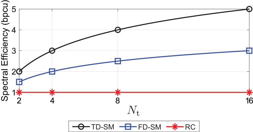
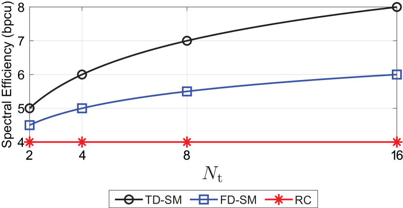
It is obvious from (9) and (15) that the amount of data carried by the constellation symbols are the same in both FD-SM and TD-SM. However, due to the time-domain encoding of the spatial symbols, the amount of data conveyed in the spatial domain is doubled in the TD-SM technique. The spectral efficiency comparisons between TD-SM, FD-SM and repetition coding (RC) are given for various numbers of transmitters, , and various signal constellation sizes, , in Fig. 6. In RC, all the LEDs transmit the same signal [11]. It is observed from Fig. 6 that TD-SM achieves the highest spectral efficiency among the considered techniques for any number of LEDs and constellation orders.
At the RX side, the optical signal is captured and translated into the electrical domain by the PDs. After analog-to-digital conversion and CP removal, the real and positive valued baseband received electrical signal vector per time instant becomes
| (16) |
where denotes the column vector of . The captured OFDM time sample is given by for . The AWGN vector is denoted by , which follows an i.i.d. Gaussian distribution, . The spatial symbols in TD-SM must be decoded in the time domain. According to [20], the channel coupling effect on the spatial symbols is simply reversed by the ZF equalizer. Please note that the performance degradation that emerges from the (near) rank deficient matrices in ZF equalization of FD-SM is completely avoided in TD-SM. The effective channel is always rank one in TD-SM as seen from (16). Therefore, the channel coupling can simply be reversed by the multiplication of reciprocals of the corresponding column vector elements. In other words, unlike FD-SM, there is always a solution for ZF equalization in TD-SM as long as . Due to the truncated Gaussian distributed characteristics of the time domain samples, the ZF detector proposed in [20] becomes sub-optimal. In [21], the optimal MAP estimator which jointly detects the transmitted samples and the LED indexes is proposed. Note that the optimal MAP estimator utilizes the PDF of the time domain samples as well as the variance of the effective noise in the estimation process. The MAP estimator used to detect the time domain samples is formulated by
| (17) |
If we plug (7) into (17), and after simple manipulations, the MAP estimation of the transmitted sample becomes
| (18) |
By taking the derivative of (18) and equating it to zero, we obtain the joint estimation of the sample value and active LED index as follows:
| (19) |
Note that (19) is conditioned on . Hence, the active LED index is estimated by the minimization of the MAP metric, , given in (18). After substituting in by (19), the estimated active LED index becomes
| (20) |
Then, the transmitted OFDM sample value is determined by plugging (20) back into (19). For further clarity, the joint MAP estimation procedure is summarized in Algorithm 1. Then, the FFT of the estimated samples vector is taken by using . Finally, the transmitted user bits are recovered by demapping and jointly.
V Experimental Set-up and Methodology
In this section, the OFDM-based optical SM experimental set-up is explained along with the corresponding methodology for evaluating the performance of the system.
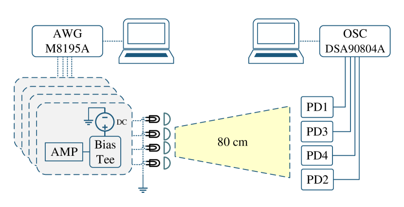
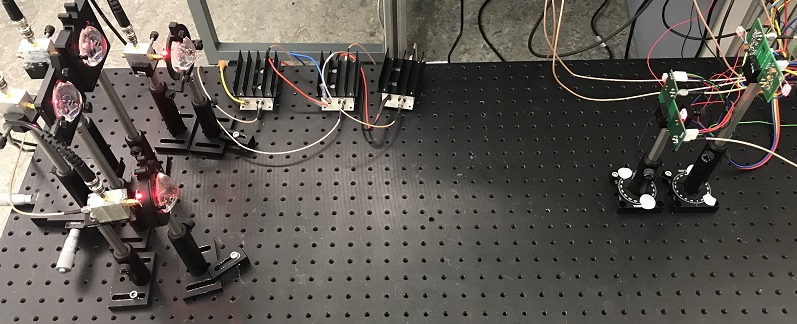
The block diagram and the photo of the experimental set-up are shown in Figs. 7(a) and 7(b), respectively. In the setup, , VLMS1500-GS08 red LEDs are used where a Thorlabs ACL4532 aspheric condenser lens is placed in front of each LED to collimate the output light of the LED. Then, four digital signals are created in MATLAB using a laptop according to methods described in previous sections (i.e., TD-SM or FD-SM). In order to comply with the flat frequency response assumption, only 20 MHz of modulation bandwidth is considered. Four channels of a high speed arbitrary waveform generator (AWG), Keysight M8195A, is used to generate analog signals from the incoming digital samples. The sampling rate of the AWG is 16 GSa/s and the resolution of the built-in digital-to-analog converter (DAC) unit is 8 bits. Signals generated by the AWG are amplified by Mini-Circuits ZHL-1A-S+ amplifier modules (AMP). The DC bias voltage and the forward current of LEDs are fixed at 2.3 V and 100 mA, respectively, which are controlled by a DC power supply. These values are chosen to minimize the nonlinear effect of LEDs. The DC bias is superimposed with the analog information carrying signal through a bias-tee module, Mini-Circuits ZFBT-4R2GW and the resulting signal is fed to the LEDs. The link distance between the TX and RX is 80 cm.
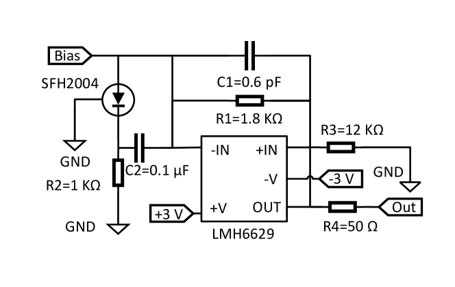
At the receiver, , LEC-RP0508 high sensitivity positive-intrinsic-negative (PIN) PDs are used in four receiver circuits as shown in Fig. 8. An operational amplifier chip, Texas Instruments LMH6629, is incorporated into the circuit. Subsequently, signals are captured by four channels of the Agilent DSA90804A high-speed oscilloscope (OSC). Lastly, the captured signals are sent to the laptop for post-processing in MATLAB.
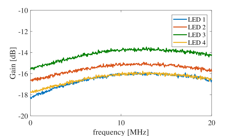
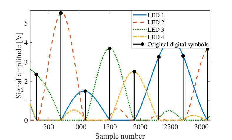
The channel matrix is estimated by training sequences, e.g., known OFDM symbols, prior to data transmission. Note that any error in the channel estimation may degrade the system performance. It is shown in the next section that simulation results match the experimental results, and thus, channel estimation in the assumed system model does not produce large errors. Furthermore, the likelihood of significant channel estimation errors is limited due to the quasi-static characteristics of the indoor optical wireless communications channel. The channel states remain stationary since the experimental setup does not include any moving components or other factors that may alter the channel condition. Therefore, an accurate initial channel estimation is valid throughout the signal transmission. The strongest front-end channel frequency responses, including the optical and electrical components, are shown in Fig. 9 for each pair of transmitters and receivers. It is observed that frequency responses of the front-end system are almost flat within a 20 MHz modulation bandwidth, i.e., the frequency response stays within the 3 dB margin. The noise variance is estimated by comparing the oversampled received signal and the known transmitted signal. The estimated value is used for TD-SM signal detection (see (19)). Part of the oversampled time domain signals and original OFDM samples for TD-SM are depicted in Fig. 10. It can be seen in Fig. 10 that at specific time samples, which are designated for data transmission and detection, only one LED transmits a non-zero value. Obviously, synchronization of signals at the TX and RX is of vital importance. In this work, synchronization at the transmitter is ensured by using the single high accuracy AWG with a built-in synchronization system. Moreover, at the beginning of each generated signal, a unique sequence of binary data is placed. The binary sequence is used to synchronize the received signals after they are captured by the oscilloscope.
As described in section IV-B and observed in Fig. 10, an LED is active (i.e., “ON”) only when it is selected according to the spatial information. Thus, if an LED is inactive (i.e., “OFF”), it must be completely turned off, meaning that the DC bias is also zero. However, as seen in Fig. 7(a), the DC bias is provided by an external DC power supply which cannot be controlled by the digital input signal. Therefore, the DC bias is constantly applied to LEDs. This is different from the theoretical system model and the TD-SM scheme. In order to solve this problem, the bipolar signal is modified before adding the DC bias. For each LED, zero values at the “OFF” time instants are replaced by a low negative value. Thus, the summation of the constant DC bias and the bipolar signal yields a very small value at the corresponding time instants. Note that this modification is only necessary due to the hardware limitation in our experimental setup, and it could be rectified in future practical implementations of the TD-SM system, where the DC bias and the signal are generated and controlled at the same time.
VI Results and discussion
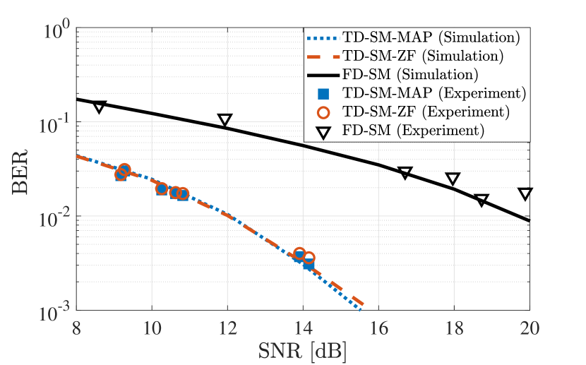
In this section, the BER performance of the described methods are compared. In order to ensure a fair comparison, the spectral efficiency of all methods is fixed at bpcu. Thus, 16-QAM and 64-QAM modulation formats are considered for TD-SM and FD-SM, respectively. The SNR is calculated as the ratio between the total received electrical power and the noise at the RX. Monte-Carlo simulation results are also presented. The optical channel gains and the noise variance obtained from the experimental results are used for Monte-Carlo simulations. The number of subcarriers and the DC bias are chosen as and dB, respectively, for both the experimental system and the computer simulations.
Firstly, the optical lenses in front of the LEDs are adjusted such that a diagonal channel matrix is realized. In other words, there is no overlap between optical links. The condition number of the channel matrix, defined as the ratio of the maximum eigenvalue to the minimum eigenvalue of the matrix, is equal to 1 in this case. The corresponding channel matrix is referred to as . Secondly, optical lenses are moved slightly in order to make the light spots larger at the receiver side so that they overlap with each other. Consequently, another channel matrix, namely , is obtained with a condition number greater than one, and in this case . In that scenario, almost 5% of the transmitted optical power from each LED is detected by two other PDs in addition to the main PD.
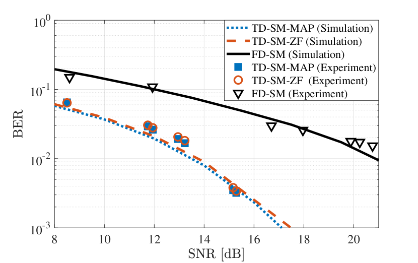
The BER performance results are presented in Figs. 11 and 12. Different SNR values are obtained by scaling the digital signal at the AWG prior to transmission. It is observed that in both scenarios, TD-SM with either MAP (TD-SM-MAP) or ZF (TD-SM-ZF) detection outperforms FD-SM by about 7 dB. It is also shown that the simulation results closely follow the experimental BER measurement for both FD-SM and TD-SM. Note that the same measured channel matrix from the experiment is used for simulations. In both Figs. 11 and 12, the BER of TD-SM-MAP is slightly lower than that of TD-SM-ZF. It is worth noting that higher SNR values would not be achievable in the experimental system due to the limited output optical power of the LEDs. In order to achieve high SNR regime, the peak-to-peak amplitude of the transmit signal has to be increased which in turn worsens the effect of nonlinearity. The nonlinearity introduced by the front-end opto-electronic devices can simply be overcome by pre-distortion of the transmit signal[53]. For the sake of brevity, both FD-SM and TD-SM systems are presented with their simplest form without loss of generality.
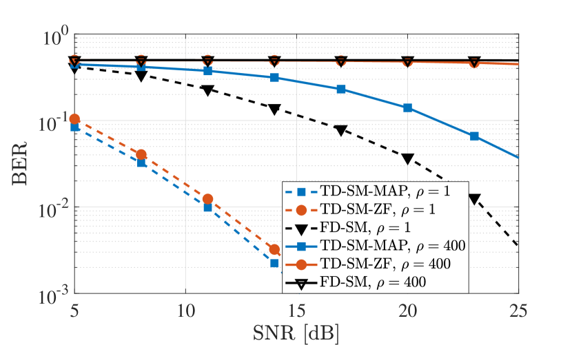
It is important to emphasize that the difference between the FD-SM and TD-SM systems would be more significant in scenarios where the channel is ill-conditioned. As mentioned in the Section IV-B and presented in [21], TD-SM exhibits inherent resilience against ill conditioned channels compared to FD-SM due to a single active LED per time instant. Thus, the effective channel in TD-SM is a column vector which is a rank one system. However, due to physical limitations in the experimental setup, we were not able to realize channel matrices with condition numbers higher than 3.5. Moreover, a larger overlap between different links (i.e., a larger light spot at the RX) significantly decreased the received optical power, and consequently, all system structures could only be realized in their low SNR regime. Hence, the experimental demonstration of such scenarios is the subject of future work. In [53], it is shown that a larger array of transmitters and receivers may also change the channel condition number. In order to investigate this case, simulation results for a 1616 system are presented in Fig. 13 with bpcu and two different channel condition numbers of and . To achieve the same spectral efficiency, 64-QAM and 4-QAM modulation formats are employed in FD-SM and TD-SM, respectively. It is observed that TD-SM-MAP achieves the lowest BER in both channel conditions. For the case, TD-SM with either MAP or ZF results in significantly lower BER compared to FD-SM due to the lower modulation order . A different behavior is observed for the case. While both FD-SM and TD-SM-ZF fail, TD-SM-MAP demonstrates better performance because it benefits from MAP detection.
In future work, the effect of temporal dispersion and intersymbol interference (i.e., effectively a frequency selective channel) on both FD-SM and TD-SM will be investigated. As the spatial symbols only exist in the time domain in TD-SM, a joint time-frequency domain detector will also be investigated to resolve the issue.
VII Conclusion
In this paper, two of the major OFDM-based optical SM techniques, namely FD-SM and TD-SM were investigated. The spatial symbols are encoded in the subcarrier level in FD-SM which brings ICI, TX/RX complexity and spectral efficiency loss. Conversely, in TD-SM technique, the spatial symbols are encoded in the time domain as suggested by conventional SM. It has been shown that TD-SM inherits all the merits of conventional SM. Moreover, TD-SM techniques achieve significantly higher spectral efficiency compared to FD-SM. Both systems have been validated in terms of BER performance by Monte Carlo computer simulations as well as, for the first time ever, experimental results. It has also been shown by using extensive simulations and demonstrating the proof-of-concept experimental results that the TD-SM with an optimal MAP detector outperforms FD-SM in terms of the BER performance. Consequently, the experimental results verify and suggest that TD-SM is a viable candidate for next-generation OFDM-based SM.
Acknowledgment
Professor Haas gratefully acknowledge the support of this research by the Engineering and Physical Sciences Research Council (EPSRC) under an Established Career Fellowship grant, EP/R007101/1. He also acknowledges the financial support of his research by the Wolfson Foundation and the Royal Society. Anil Yesilkaya acknowledges financial support for his PhD studies from Zodiac Inflight Innovations (TriaGnoSys GmbH). The authors would like to thank Dr. Tezcan Cogalan and Dr. Hossein Kazemi for their insightful comments and suggestions.
References
- [1] “Cisco visual networking index: Global mobile data traffic forecast update, 2016–2021 white paper, [Online],” https://www.cisco.com/c/en/us/solutions/collateral/service-provider/visual-networking-index-vni/mobile-white-paper-c11-520862.pdf, accessed: 30-04-2019.
- [2] T. Cogalan and H. Haas, “Why would 5G need optical wireless communications?” in Proc. 2017 IEEE 28th Ann. Int. Symp. Personal, Indoor Mobile Radio Commun. (PIMRC), Oct. 2017, pp. 1–6.
- [3] H. Haas, L. Yin, Y. Wang, and C. Chen, “What is LiFi?” J. Lightw. Technol., vol. 34, no. 6, pp. 1533–1544, Mar. 2016.
- [4] I. Stefan, H. Burchardt, and H. Haas, “Area spectral efficiency performance comparison between VLC and RF femtocell networks,” in Proc. 2013 IEEE Int. Conf. Commun. (ICC), Jun. 2013, pp. 3825–3829.
- [5] M. D. Soltani, X. Wu, M. Safari, and H. Haas, “Bidirectional user throughput maximization based on feedback reduction in LiFi networks,” IEEE Trans. Commun., vol. 66, no. 7, pp. 3172–3186, Jul. 2018.
- [6] D. Takase and T. Ohtsuki, “Optical wireless MIMO communications (OMIMO),” in 2004 IEEE Global Commun. Conf. (GLOBECOM), vol. 2, Dallas, TX, USA, Nov. 2004, pp. 928–932.
- [7] S. Hranilovic and F. R. Kschischang, “A pixelated MIMO wireless optical communication system,” IEEE J. Sel. Topics in Quantum Electron., vol. 12, no. 4, pp. 859–874, Jul. 2006.
- [8] D. O’Brien, “Multi-input multi-output (MIMO) indoor optical wireless communications,” in Proc. 2009 Asilomar Conf. Signals, Syst. Comp., Nov 2009, pp. 1636–1639.
- [9] L. Zeng, D. C. O’Brien, H. L. Minh, G. E. Faulkner, K. Lee, D. Jung, Y. Oh, and E. T. Won, “High data rate multiple input multiple output (MIMO) optical wireless communications using white LED lighting,” IEEE J. Sel. Areas Commun., vol. 27, no. 9, pp. 1654–1662, Dec. 2009.
- [10] K. D. Dambul, D. C. O’Brien, and G. Faulkner, “Indoor optical wireless MIMO system with an imaging receiver,” IEEE Photon. Tech. Lett., vol. 23, no. 2, pp. 97–99, Jan. 2011.
- [11] T. Fath and H. Haas, “Performance comparison of MIMO techniques for optical wireless communications in indoor environments,” IEEE Trans. Commun., vol. 61, no. 2, pp. 733–742, Feb. 2013.
- [12] D. Tsonev, S. Sinanovic, and H. Haas, “Practical MIMO capacity for indoor optical wireless communication with white LEDs,” in Proc. IEEE Veh. Technol. Conf. (VTC Spring), Jun. 2013, pp. 1–5.
- [13] H. Haas, E. Costa, and E. Schulz, “Increasing spectral efficiency by data multiplexing using antenna arrays,” in Proc. 13th IEEE Int. Symp. Pers. Indoor Mobile Radio Commun., vol. 2, Pavilhao Altantico, Lisboa, Portugal, Portugal, Sep. 2002, pp. 610–613 vol.2.
- [14] R. Mesleh, H. Haas, Y. Lee, and S. Yun, “Interchannel interference avoidance in MIMO transmission by exploiting spatial information,” in Proc. IEEE 16th Int. Symp. on Personal, Indoor and Mobile Radio Commun., vol. 1, Berlin, Germany, Sep. 2005, pp. 141–145.
- [15] R. Mesleh, H. Haas, C. W. Ahn, and S. Yun, “Spatial modulation - a new low complexity spectral efficiency enhancing technique,” in Proc. 1st Int. Conf. Commun. Netw. in China, Beijing, China, Oct. 2006, pp. 1–5.
- [16] S. Ganesan, R. Mesleh, H. Haas, C. W. Ahn, and S. Yun, “On the performance of spatial modulation OFDM,” in Proc. 40th Asilomar Conf. on Signals, Syst. and Comput., Pacific Grove, CA, USA, Oct. 2006, pp. 1825–1829.
- [17] R. Y. Mesleh, H. Haas, S. Sinanovic, C. W. Ahn, and S. Yun, “Spatial modulation,” IEEE Trans. Veh. Technol., vol. 57, no. 4, pp. 2228–2241, Jul. 2008.
- [18] M. D. Renzo, H. Haas, A. Ghrayeb, S. Sugiura, and L. Hanzo, “Spatial modulation for generalized MIMO: Challenges, opportunities, and implementation,” Proc. IEEE, vol. 102, no. 1, pp. 56–103, Jan. 2014.
- [19] X. Zhang, S. Dimitrov, S. Sinanovic, and H. Haas, “Optimal power allocation in spatial modulation OFDM for visible light communications,” in Proc. IEEE Veh. Technol. Conf. (VTC Spring), Yokohama, Japan, May 2012, pp. 1–5.
- [20] P. Butala, H. Elgala, and T. D. C. Little, “Sample indexed spatial orthogonal frequency division multiplexing,” Chin. Opt. Lett., vol. 12, no. 9, p. 090602, Sep. 2014.
- [21] I. Tavakkolnia, A. Yesilkaya, and H. Haas, “OFDM-based spatial modulation for optical wireless communications,” in 2018 IEEE Globecom Workshops (GC Wkshps), 2018.
- [22] Y. Li, D. Tsonev, and H. Haas, “Non-DC-biased OFDM with optical spatial modulation,” in Proc. IEEE 24th Ann. Int. Symp. Personal, Indoor Mobile Radio Commun. (PIMRC), London, UK, Sep. 2013, pp. 486–490.
- [23] C. Chen, W. Zhong, and D. Wu, “Non-Hermitian symmetry orthogonal frequency division multiplexing for multiple-input multiple-output visible light communications,” IEEE/OSA J. Opt. Commun. Netw., vol. 9, no. 1, pp. 36–44, Jan. 2017.
- [24] E. Başar, E. Panayirci, M. Uysal, and H. Haas, “Generalized LED index modulation optical OFDM for MIMO visible light communications systems,” in Proc. 2016 IEEE Int. Conf. Commun. (ICC), May 2016, pp. 1–5.
- [25] R. Tejaswi, T. L. Narasimhan, and A. Chockalingam, “Quad-LED complex modulation (QCM) for visible light wireless communication,” in Proc. 2016 IEEE Wireless Commun. Netw. Conf. Workshops (WCNCW), Apr. 2016, pp. 18–23.
- [26] A. Yesilkaya, E. Basar, F. Miramirkhani, E. Panayirci, M. Uysal, and H. Haas, “Optical MIMO-OFDM with generalized LED index modulation,” IEEE Trans. Commun., vol. 65, no. 8, pp. 3429–3441, Aug. 2017.
- [27] M. Ijaz, D. Tsonev, A. Stavridis, A. Younis, J. J. D. McKendry, E. Gu, M. D. Dawson, S. Videv, and H. Haas, “Optical spatial modulation OFDM using micro LEDs,” in Proc. 2014 48th Asilomar Conf. Signals, Syst. Comput., Nov 2014, pp. 1734–1738.
- [28] M. Ijaz, D. Tsonev, J. J. D. McKendry, E. Xie, S. Rajbhandari, H. Chun, G. Faulkner, E. Gu, M. D. Dawson, D. O’Brien, and H. Haas, “Experimental proof-of-concept of optical spatial modulation OFDM using micro LEDs,” in Proc. 2015 IEEE Int. Conf. Commun. Workshop (ICCW), Jun. 2015, pp. 1338–1343.
- [29] C. He, T. Q. Wang, and J. Armstrong, “Performance comparison between spatial multiplexing and spatial modulation in indoor MIMO visible light communication systems,” in 2016 IEEE Int. Conf. on Commun. (ICC), Kuala Lumpur, Malaysia, May 2016, pp. 1–6.
- [30] M. L. Tran, S. Kim, T. Ketseoglou, and E. Ayanoglu, “LED selection and MAP detection for generalized LED index modulation,” IEEE Photon. Technol. Lett., vol. 30, no. 19, pp. 1695–1698, Oct. 2018.
- [31] D. Slepian, “Permutation modulation,” Proc. of the IEEE, vol. 53, no. 3, pp. 228–236, Mar. 1965.
- [32] E. J. Baghdady, “Directional signal modulation by means of switched spaced antennas,” IEEE Trans. Commun., vol. 38, no. 4, pp. 399–403, Apr. 1990.
- [33] Y. A. Chau and S.-H. Yu, “Space modulation on wireless fading channels,” in Proc. IEEE Veh. Technol. Conf. (VTC Fall), vol. 3, Atlantic City, NJ, USA, USA, Oct. 2001, pp. 1668–1671 vol.3.
- [34] S. Song, Y. Yang, Q. Xionq, K. Xie, B.-J. Jeong, and B. Jiao, “A channel hopping technique I: theoretical studies on band efficiency and capacity,” in 2004 Int. Conf. Commun., Circuits and Syst., vol. 1, Chengdu, China, Jun. 2004, pp. 229–233 Vol.1.
- [35] J. Jeganathan, A. Ghrayeb, and L. Szczecinski, “Generalized space shift keying modulation for MIMO channels,” in Proc. IEEE 19th Int. Symp. Pers. Indoor Mobile Radio Commun., Cannes, France, Sep. 2008, pp. 1–5.
- [36] A. Younis, N. Serafimovski, R. Mesleh, and H. Haas, “Generalised spatial modulation,” in Proc. 44th Asilomar Conf. Signals, Syst. Comput., Pacific Grove, CA, USA, Nov 2010, pp. 1498–1502.
- [37] J. Fu, C. Hou, W. Xiang, L. Yan, and Y. Hou, “Generalised spatial modulation with multiple active transmit antennas,” in Proc. IEEE GLOBECOM Workshops, Miami, FL, USA, Dec. 2010, pp. 839–844.
- [38] N. Serafimovski, M. D. Renzo, S. Sinanovic, R. Y. Mesleh, and H. Haas, “Fractional bit encoded spatial modulation (FBE-SM),” IEEE Commun. Lett., vol. 14, no. 5, pp. 429–431, May 2010.
- [39] S. Sugiura, S. Chen, and L. Hanzo, “Coherent and differential space-time shift keying: A dispersion matrix approach,” IEEE Trans. Commun., vol. 58, no. 11, pp. 3219–3230, Nov. 2010.
- [40] J. Wang, S. Jia, and J. Song, “Generalised spatial modulation system with multiple active transmit antennas and low complexity detection scheme,” IEEE Trans. Wireless Commun., vol. 11, no. 4, pp. 1605–1615, Apr. 2012.
- [41] W. Popoola, E. Poves, and H. Haas, “Generalised space shift keying for visible light communications,” in Proc. 8th Int. Symp. Commun. Syst., Netw. Digit. Signal Process. (CSNDSP), Poznan, Poland, Jul. 2012, pp. 1–4.
- [42] R. Mesleh, S. S. Ikki, and H. M. Aggoune, “Quadrature spatial modulation,” IEEE Trans. Veh. Technol., vol. 64, no. 6, pp. 2738–2742, Jun. 2015.
- [43] C. Cheng, H. Sari, S. Sezginer, and Y. T. Su, “Enhanced spatial modulation with multiple signal constellations,” IEEE Trans. Commun., vol. 63, no. 6, pp. 2237–2248, Jun. 2015.
- [44] M. D. Renzo, H. Haas, and P. M. Grant, “Spatial modulation for multiple-antenna wireless systems: a survey,” IEEE Commun. Mag., vol. 49, no. 12, pp. 182–191, Dec. 2011.
- [45] M. D. Renzo and H. Haas, “Space shift keying (SSK) modulation with partial channel state information: Optimal detector and performance analysis over fading channels,” IEEE Trans. Commun., vol. 58, no. 11, pp. 3196–3210, Nov. 2010.
- [46] ——, “A general framework for performance analysis of space shift keying (SSK) modulation for MISO correlated Nakagami-m fading channels,” IEEE Trans. Commun., vol. 58, no. 9, pp. 2590–2603, Sep. 2010.
- [47] R. Mesleh, R. Mehmood, H. Elgala, and H. Haas, “Indoor MIMO optical wireless communication using spatial modulation,” in 2010 IEEE International Conference on Communications, May 2010, pp. 1–5.
- [48] K. Ntontin, M. D. Renzo, A. Perez-Neira, and C. Verikoukis, “Performance analysis of multistream spatial modulation with maximum-likelihood detection,” in Proc. IEEE Global Commun. Conf. (GLOBECOM), Atlanta, GA, USA, Dec. 2013, pp. 1590–1594.
- [49] C. Chen, D. A. Basnayaka, and H. Haas, “Downlink performance of optical attocell networks,” J. Lightw. Technol., vol. 34, no. 1, pp. 137–156, Jan. 2016.
- [50] J. M. Kahn and J. R. Barry, “Wireless infrared communications,” Proc. IEEE, vol. 85, no. 2, pp. 265–298, Feb. 1997.
- [51] T. Komine and M. Nakagawa, “Integrated system of white LED visible-light communication and power-line communication,” IEEE Trans. Consum. Electron., vol. 49, no. 1, pp. 71–79, Feb. 2003.
- [52] S. Hranilovic, Wireless Optical Communication Systems. Springer, 1996.
- [53] S. Dimitrov and H. Haas, “Information rate of OFDM-based optical wireless communication systems with nonlinear distortion,” J. Lightw. Technol., vol. 31, no. 6, pp. 918–929, Mar. 2013.
![[Uncaptioned image]](/html/1911.10380/assets/graphics/bio/yesilkaya_bw.png) |
Anil Yesilkaya (S’11) received the B.Sc (1st Hons) and M.Sc degrees in electronics engineering from the Kadir Has University, Istanbul, Turkey in 2014 and 2016, respectively. He was the recipient of the Best Paper Award at the IEEE International Conference on Communications, in 2018. He is currently pursuing the Ph.D. degree in digital communications with the University of Edinburgh. His research interests include, PHY layer security, multiple-input multiple-output optical wireless communications and LiFi-based in-flight connectivity. |
![[Uncaptioned image]](/html/1911.10380/assets/graphics/bio/bian_bw.png) |
Rui Bian received the B.Eng. degree in information engineering from the Wuhan University of Technology, Wuhan, China, in 2011, and the M.Sc. degree in electronics from the University of Edinburgh, Edinburgh, U.K., in 2013, where he is currently pursuing the Ph.D. degree in digital communications. His main research interest is in visible light communication. |
![[Uncaptioned image]](/html/1911.10380/assets/graphics/bio/tavakkolnia_bw.png) |
Iman Tavakkolnia (S’15–M’18) received the B.Sc. degree in telecommunication engineering from the University of Tehran, Tehran, Iran, in 2006, the M.Sc. degree in communication systems from the Sharif University of Technology, Tehran, Iran, in 2011, and the Ph.D. degree in electrical engineering from the University of Edinburgh, Edinburgh, U.K., in 2018. He is currently a Research Associate with LiFi Research and Development Centre, University of Edinburgh. His research interests include communication theory, optical fiber communication, and visible light communication. |
![[Uncaptioned image]](/html/1911.10380/assets/graphics/bio/haas_bw.jpg) |
Harald Haas (S’98-AM’00-M’03-SM’16-F’17) received the Ph.D. degree from The University of Edinburgh in 2001. He is currently the Chair of Mobile Communications at The University of Edinburgh, and he is the Initiator, Co-Founder, and Chief Scientific Officer of pureLiFi Ltd., and the Director of the LiFi Research and Development Centre, The University of Edinburgh. He has authored 430 conference and journal papers, including a paper in Science and co-authored a book Principles of LED Light Communications Towards Networked Li-Fi (Cambridge University Press, 2015). His main research interests are in optical wireless communications, hybrid optical wireless and RF communications, spatial modulation, and interference coordination in wireless networks. He first introduced and coined spatial modulation and LiFi. LiFi was listed among the 50 best inventions in TIME Magazine in 2011. He was an invited speaker at TED Global 2011, and his talk on Wireless Data from Every Light Bulb has been watched online over 2.4 million times. He gave a second TED Global lecture in 2015 on the use of solar cells as LiFi data detectors and energy harvesters. This has been viewed online over 2 million times. He was elected as a fellow of the Royal Society of Edinburgh and a Fellow of the IEEE in 2017. In 2012 and 2017, he was a recipient of the prestigious Established Career Fellowship from the Engineering and Physical Sciences Research Council (EPSRC) within Information and Communications Technology in the U.K. In 2014, he was selected by EPSRC as one of ten Recognizing Inspirational Scientists and Engineers Leaders in the U.K. He was a corecipient of the EURASIP Best Paper Award for the Journal on Wireless Communications and Networking in 2015 and the Jack Neubauer Memorial Award of the IEEE Vehicular Technology Society. In 2016, he received the Outstanding Achievement Award from the International Solid State Lighting Alliance. He was a co-recipient of recent best paper awards at VTC-Fall, 2013, VTC-Spring 2015, ICC 2016, ICC 2017 and ICC 2018. He is an Editor of the IEEE TRANSACTIONS ON COMMUNICATIONS and the IEEE JOURNAL OF LIGHTWAVE TECHNOLOGIES. |