Observation of optical absorption correlated with surface state of topological insulator
Abstract
We performed broadband optical transmission measurements of Bi2Se3 and In-doped thin films, where in the latter the spin-orbit coupling (SOC) strength can be tuned by introducing In. Drude and interband transitions exhibit In-dependent changes that are consistent with evolution from metallic (x=0) to insulating (x=1) nature of the end compounds. Most notably, an optical absorption peak located at =1eV in Bi2Se3 is completely quenched at x=0.06, the critical concentration where the phase transition from TI into non-TI takes place. For this x, the surface state (SS) is vanished from the band structure as well. The correlation between the 1eV optical peak and the SS in the x-dependences suggests that the peak is associated with the SS. We further show that when Bi2Se3 is electrically gated, the 1eV-peak becomes stronger(weaker) when electron is depleted from (accumulated into) the SS. These observations combined together demonstrate that under the =1eV illumination electron is excited from a bulk band into the topological surface band of Bi2Se3. The optical population of surface band is of significant importance not only for fundamental study but also for TI-based optoelectronic device application.
pacs:
68.65.Pq 78.30.-j 78.67.WjIntroduction. Topological insulator (TI) is a novel state of matter characterized by insulating bulk and metallic surfaceFu et al. (2007); Xia et al. (2009); Hasan and Kane (2010); Moore (2010); Qi and Zhang (2011). The surface state, topologically protected and chirally-textured, supports dissipationless spin-conserving current, applicable for quantum devicesRoushan et al. (2009); Hsieh et al. (2009); Li et al. (2014). Optically, various kinds of electron transitions occur in a TI under photo illumination both in the surface and in the bulk as demonstrated by numerous previous experiments: For the archetypal TI material Bi2Se3, intraband (Drude) transition and Kerr rotation of the surface carrier were observed in THz measurement Aguilar et al. (2012). In the infrared range, Post et al measured the interband transition from bulk valence-band (VB) to bulk conduction-band (CB), VBCB, and determined upper bound of Drude weight of SS Post et al. (2015). Also Falsetti et al observed the infrared Berreman resonance of the surface electron in Bi2Se3 thin films Falsetti et al. (2018). On the other hand, for periodically modulated Bi2Se3, plasmonic excitation of the surface electron Di Pietro et al. (2013) and the plasmon-phonon interaction In et al. (2018) were observed at THz frequencies.
One interesting optical absorption that TI can host yet has not been detected is an excitation of electron from bulk band into SS. This particular transition between bulk and surface, VBSS, will provide rare opportunity to study how the surface and bulk are connected optically. Also, when the surface electron is populated by this optical transition, the surface electron is increased and therefore the topological current ( surface electron) is enhanced, which can boost the performance of TI as optoelectronic device such as photogalvanics and optical imaging display McIver et al. (2012); Yue et al. (2017). In fact Sobota et al showed that a similar transition can occur from bulk CB to 2nd SS, CB2nd SS, at a visible frequency Sobota et al. (2013). (Here the 2nd SS refers to another SS that lies above the 1st or fundamental SS). However the optical transition into the 1st SS or fundamental SS, VBSS, was not reported yet. It is not clear at this point whether the lack of the SS-populating optical transition is due to that other transition such as VBCB is overwhelmingly stronger, making the detection difficult Li et al. (2015), or more fundamentally, this particular transition is forbidden by optical selection rule.
Here we performed broadband optical absorption measurement of Bi2Se3 and thin films from far-IR to UV frequencies.
In , the spin-orbit coupling (SOC) strength is modulated by means of
the indium (In) substitution. As In-content is increased the SOC of Bi2Se3 is decreased
and consequently the topological property is softened. Eventually,
at certain substitution level, the topological SS is completely quenched from the band structure. Accordingly any SS-related optical transition will be removed from the wide-range optical excitation spectrum, which
in fact offers us an invaluable means to find the SS-population transition in particular.
Our measurement shows signatures that such optical absorption may exist.
Experiment.
High quality epitaxial Bi2Se3 and thin films were grown on
Al2O3 and SiO2/Si substrates using the
MBE method Bansal et al. (2011). Optical transmittance T()
was measured from Far-infrared to UV by using Fourier transform infrared spectroscopy (FTIR) spectrometer
in combination with spectroscopic ellipsometer. For gate-dependent optical measurement
gate-voltage was applied between and Si of the substrate.
Optical conductivity was calculated from transmission data
through rigorous Kramers-Kronig transformation by using RefFitKuzmenko (2005). The experimental details are described in Supplemental Material 1sup and references therein.
Results.
Figure 1 shows the wide-range optical conductivity of
the 50QL-thick film.
In the Far-infrared region, consists of Drude absorption and optical phonon peak, both
coming from the bulk, where the former one arises from the Se-vacancy driven carrier Post et al. (2013); Di Pietro et al. (2012).
For 0.25eV, the interband (IB) transition VBCB leads to
the rapid rise of .
Note that there is an absorption peak at =1eV
(Peak-A hereafter) which we will pay particular attention to.
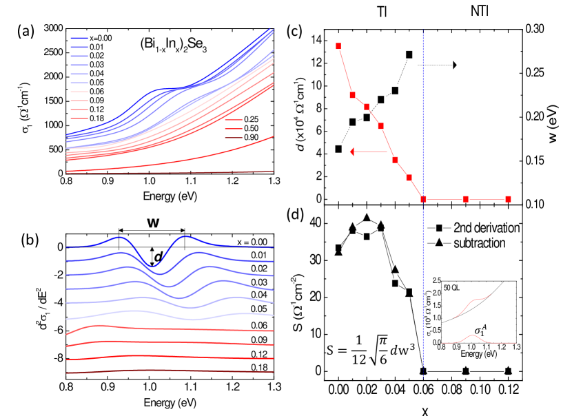
In Figure 2 we show optical conductivity measured for a series of In-substituted films. The In-concentration was varied for 0x0.9 range.
Previous studies showed that as Bi is replaced by the light element In, the spin-orbit interaction
is reduced and the topological property of Bi2Se3 becomes weaker Brahlek et al. (2012); Salehi et al. (2016); Wu et al. (2013); Sim et al. (2015).
At a critical concentration xc,
phase transition from TI to non-TI (NTI) phase occurs where the bulk band gap is closed, and CB and VB begin to reinvert. The xc lies between x=0.04 and x=0.06
depending on the film thickness, and for at xxc the topological SS is completely vanished Brahlek et al. (2012); Salehi et al. (2016). The
shows that Peak-A becomes weaker
as increases. For quantitative analysis of this behavior
we isolate Peak-A by removing background conductivity from as
=-
as illustrated in the inset of Figure 2d, (a polynomial function was used for the )
and calculated the strength of Peak-A as =.
Figure 2d
shows that is quenched at x=0.06. To double check this behavior
we performed independent analysis of Peak-A:
we calculate the second derivative
and measure the distance (w) and depth () of the extrema pattern, which allows
determination of strength (=dw3) as well as width (= w) and height (= dw2) of Peak-A. (See Supplemental Fig. S1 for detailssup ).
The is quenched at x=0.06 again, which confirms the = analysis.
Importantly x=0.06
is the critical xc for the TINTI transition for the thickness =50QL of our films: that is, the SS is vanished at this x. This correlation of Peak-A with the TINTI transition
strongly suggests that Peak-A is related with the topological SS of Bi2Se3. We emphasize that this behavior is strikingly different from those of the other optical absorption features:
In Supplemental Fig.S2sup , we show that the Drude absorption is
vanished at x0.5, the phonon peak splits at x= 0.12, and the IB survives up to x=0.9.
(For x=1, is a large gap band insulator with 1.5eV)
Note that none of these features are correlated with xc. In contrast
Peak-A manifests clear correlation with xc and is the only absorption of such kind.
Given the correlation of Peak-A with SS, one can propose possible pictures on how Peak-A is created. Specifically, Peak-A can arise when (1) SS electron is excited into
empty state lying 1eV above, or alternatively
(2) electron lying at 1eV below is excited into the SS. In both scenarios
Peak-A becomes extinct when SS is suppressed at xc.
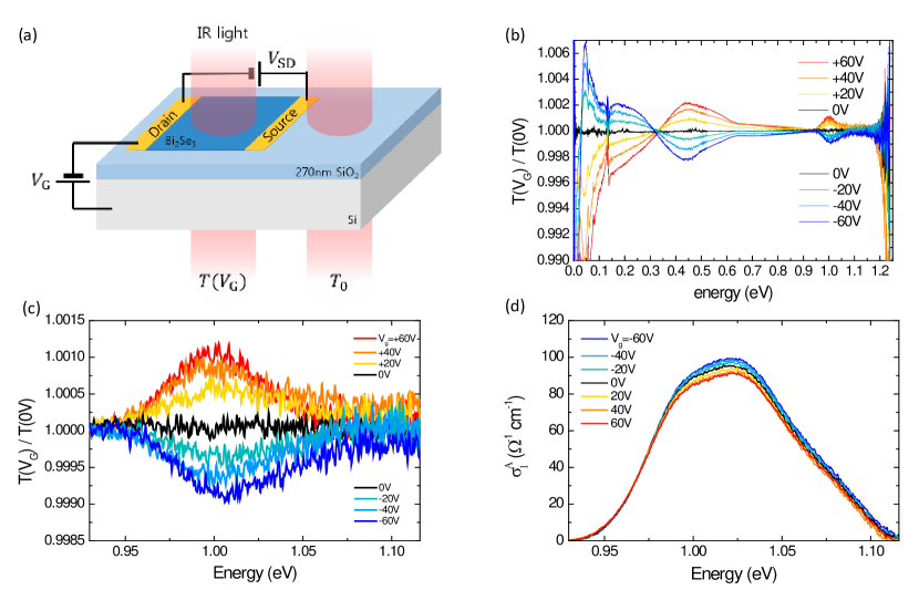
To find out which scenario is correct, we performed electrical gating experiment on the Bi2Se3 film (=8QL).
For this a Bi2Se3 film was grown on SiO2/Si substrate and optical transmission was measured while gate voltage is applied between the film and Si.
In this back-gate configuration, the Fermi energy EF shifts down (up)
for the negative (positive) due to electron depletion (accumulation) in the film.
Fig.3(b) shows that T()/T(0) changes in the Far-IR, mid-IR, and at 1eV.
Figure 3(c) shows that
Peak-A becomes stronger (weaker) for negative (positive) . Such change
supports the scenario (2) over (1) for the following reason: For 0 the electron occupation of SS is
reduced and more empty SS become available, which strengthens the transition of (2), which
agrees with
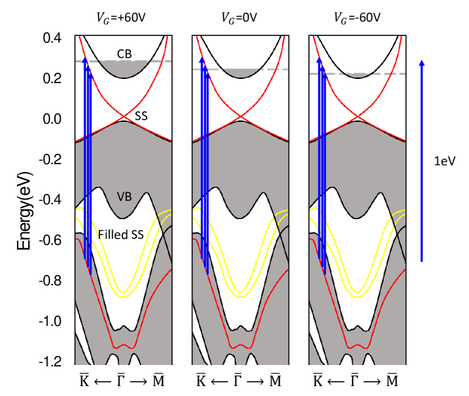
the increase of Peak-A strength. This relation is visualized in Fig.4. In the scenario (1), on the other hand, the surface electron is decreased and
the peak becomes weaker, opposite to the observed behavior of Peak-A.
Therefore, the -dependent result demonstrates that Peak-A arises most likely by excitation of electron from a state lying 1eV below into the SS. In this transition electron occupation of SS is increased, or equally,
the SS is optically populated by illuminating Bi2Se3 with =1eV.
Here we remark that
the -dependent change in Figure 3c is very small, less than even 0.1%.
Nevertheless the Peak-A change is successfully measured, demonstrating the superior sensitivity and stability of our experiment.
For later analysis
we calculate the -dependent from the T()/T(0) data
Yu et al. (2016, 2019a, 2019b) and show it in Figure 3(d).
With the nature of Peak-A been identified, the next question to be addresed is the origin of the initial state. Before we discuss
this issue, we give further thoughts on the gate-dependent growth of Peak-A. Figure 3 implies that
the SS-population will become stronger if EF could be brought down further. The latter would be possible when is applied to high value beyond the limit of our measurement, where such high-gating was in fact demonstrated experimentally Bansal et al. (2014). Here we will consider how
large Peak-A will grow in the strong-gating regime.
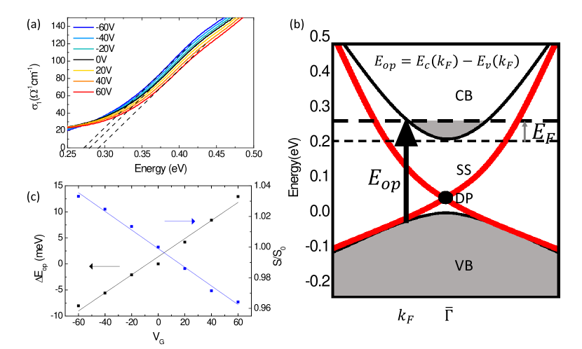
In Figure 4a, we show the bulk interband transition in the mid-IR range.
The onset energy (Eop) of this transition corresponds to the thick arrow in Fig.4(b).
The Eop increases when the Fermi level shifts up. Fig.4(c) shows that
the increase rate is dEop/d =1.74[eV/V].
In the mean time
the = calculated from Figure3(d) decreases
at the rate
d/d =-6.06[1/V], where =S/S(0V) is the normalized by
ungated .
Given and
we can eliminate and obtain the S-change against EF as d/dEF = (d/d)(d/dEF)= /(/2)=6.96[1/eV].
Here d/dEF= was derived by utilizing the Bernstein-Moss relationBurstein (1954); Moss (1954); Hamberg et al. (1984),
namely, dEF/d= dEop/d= where
the factor comes from
and =Analytis et al. (2010).
This result d/dEF=6.96[1/eV] enables us estimate at high gating:
For the pristine, electron-doped Bi2Se3 films like ours, the Fermi level lies typically at
0.1eV from the CB bottom (CBB).
If the gating shifts down to the CBB, i.e, EF=0.1, then
will increase approximately by [] EF=0.69.
that is, Peak-A grows by 70 compared with the ungated strength.
If EF is shifted further to the Dirac point, the latter lying 0.2eV from the CBB, we have
=+1+[](0.1+0.2)=3.09.
That is, Peak-A grows as large as three-times. (Here we assumed
is constant for simplicity, neglecting its -dependence.)
This estimation shows that substantial increase of the peak will occur at high-gating.
From this exercise we also learn that if is precisely characterized as function of EF,
it could be used to determine the location of the Fermi level in Bi2Se3 films, whereas
usually more difficult ARPES should be performed.
Discussion. We now search for possible candidate for the initial state of the Peak-A. For this we refer to the band structure of Bi2Se3 reported in experimental Hsieh et al. (2009); Nechaev et al. (2013); Hasan and Kane (2010); Pan et al. (2011); Wray et al. (2010); Dubroka et al. (2017); Piot et al. (2016) and theoretical Aguilera et al. (2013); Guo et al. (2016); Förster et al. (2015); Hermanowicz and Radny (2019) literatures, and schematically redrew it in Figure5. In Figure 5 note that there is an energy branch lying 1eV below the SS. Interestingly, this branch E(k) runs in near-parallel with the SS. If we consider the optical transition from this E(k) branch (=i) to SS (=f), their parallel dispersion leads to strong absorption due to that transition strength S becomes divergent. This yields a pronounced absorption at =Ef-Ei=1eV, which agrees with the profile of Peak-A. (Here the transition matrix element Mfi is assumed to be constant for simplicity.) Therefore this 1eV-E(k) is a plausible candidate for the i-state. We think that this assignment can be confirmed when theoretical calculation of , not available currently, is performed. We remark that optical transition of Bi2Se3 between bulk and surface in particular was poorly studied so far with a rare exceptionLi et al. (2015). To consider another candidate native defect such as Se-vacancy can produce defect levels below . However their energy locations are not well known, and generally such localized, dispersionless levels do not fulfill the condition. We emphasize that, while supporting works should follow to definitely identify the 1eV-bulk E(k) as origin of i-state, the occurrence of the optical population of SS in Bi2Se3 is evident judging from the properties of Peak-A we have unveiled regardless of the i-state origin.
To make further remark on the T()/T(0) data, Fig.3(b) shows that gate-dependent change occurs in the Far-IR and mid-IR ranges also. Similar change was reported for bulk-insulating filmsWhitney et al. (2016).
While for the mid-IR modulation peaks at 0.3eV, the modulation for Bi2Se3 occurs at higher energy, peaked at 0.45 eV. This difference is attributed to that the interband transition taking place at Eop=Eg+2EF is higher for Bi2Se3 where EF is significant (0.1 eV) compared with the insulating where EF is considered to be much lower.
Also, while the modulations in mid-IR and far-IR inevitably contain contribution from both bulk and surface states, the modulation strength of the 1eV feature is weaker, which may further support the surface-related origin. Further quantitative analysis and comparison will be published separately.
In conclusion we performed broadband optical absorption measurement on pristine Bi2Se3
and In-substituted thin films, as well as electrically gated Bi2Se3. The absorption Peak-A that occurs at =1eV
showed clear correlation with the In-driven TI-NTI phase transition: it is activated at xxc (TI-phase)
but is completely vanished for xxc (NTI) along with the quenching of the topological surface state. Furthermore, the Peak-A become stronger/weaker by the electron depletion/injection into the Bi2Se3 in the electrical gating measurement.
The two experimental results provide convincing evidence that Peak-A arises from the
population of SS, i.e, the optical excitation of electron from 1eV below into into SS. This SS-optical population increases the density of the surface electron, thus can enhance the topological electrical conduction, which promotes TI device application.
Similar optically driven SS-population may be realized
in other TI materials as well, which should be investigated in the future.
Note added: For our films, the bulk transition Eop shows a different x-dependent behavior from Ref.Wu et al. (2013).
It may come from that carrier doping due to Se-vacancy is sample-dependent for these TI films. See Supplemental Fig.S3sup .
Acknowledgments. This work was supported by the 2016 sabbatical year research grant of the University of Seoul. JM and SO are supported by the Gordon and Betty Moore Foundation’s EPiQS Initiative (GBMF4418) and National Science Foundation (NSF) grant EFMA-1542798.
References
- Fu et al. (2007) L. Fu, C. L. Kane, and E. J. Mele, Physical Review Letters 98, 106803 (2007).
- Xia et al. (2009) Y. Xia, D. Qian, D. Hsieh, L. Wray, A. Pal, H. Lin, A. Bansil, D. Grauer, Y. S. Hor, R. J. Cava, et al., Nature Physics 5, 398 (2009).
- Hasan and Kane (2010) M. Z. Hasan and C. L. Kane, Reviews of Modern Physics 82, 3045 (2010).
- Moore (2010) J. E. Moore, Nature 464, 194 (2010).
- Qi and Zhang (2011) X.-L. Qi and S.-C. Zhang, Reviews of Modern Physics 83, 1057 (2011).
- Roushan et al. (2009) P. Roushan, J. Seo, C. V. Parker, Y. S. Hor, D. Hsieh, D. Qian, A. Richardella, M. Z. Hasan, R. J. Cava, and A. Yazdani, Nature 460, 1106 (2009).
- Hsieh et al. (2009) D. Hsieh, Y. Xia, D. Qian, L. Wray, J. Dil, F. Meier, J. Osterwalder, L. Patthey, J. Checkelsky, N. Ong, et al., Nature 460, 1101 (2009).
- Li et al. (2014) C. Li, O. Van‘t Erve, J. Robinson, Y. Liu, L. Li, and B. Jonker, Nature Nanotechnology 9, 218 (2014).
- Aguilar et al. (2012) R. V. Aguilar, A. Stier, W. Liu, L. Bilbro, D. George, N. Bansal, L. Wu, J. Cerne, A. Markelz, S. Oh, et al., Physical Review Letters 108, 087403 (2012).
- Post et al. (2015) K. Post, B. Chapler, M. Liu, J. Wu, H. Stinson, M. Goldflam, A. Richardella, J. Lee, A. Reijnders, K. Burch, et al., Physical Review Letters 115, 116804 (2015).
- Falsetti et al. (2018) E. Falsetti, A. Nucara, P. P. Shibayev, M. Salehi, J. Moon, S. Oh, J.-B. Brubach, P. Roy, M. Ortolani, and P. Calvani, Physical Review Letters 121, 176803 (2018).
- Di Pietro et al. (2013) P. Di Pietro, M. Ortolani, O. Limaj, A. Di Gaspare, V. Giliberti, F. Giorgianni, M. Brahlek, N. Bansal, N. Koirala, S. Oh, et al., Nature Nanotechnology 8, 556 (2013).
- In et al. (2018) C. In, S. Sim, B. Kim, H. Bae, H. Jung, W. Jang, M. Son, J. Moon, M. Salehi, S. Y. Seo, et al., Nano Letters 18, 734 (2018).
- McIver et al. (2012) J. McIver, D. Hsieh, H. Steinberg, P. Jarillo-Herrero, and N. Gedik, Nature Nanotechnology 7, 96 (2012).
- Yue et al. (2017) Z. Yue, G. Xue, J. Liu, Y. Wang, and M. Gu, Nature Communications 8, 15354 (2017).
- Sobota et al. (2013) J. A. Sobota, S.-L. Yang, A. F. Kemper, J. Lee, F. T. Schmitt, W. Li, R. G. Moore, J. G. Analytis, I. R. Fisher, P. S. Kirchmann, et al., Physical Review Letters 111, 136802 (2013).
- Li et al. (2015) L. Li, W. Xu, and F. Peeters, Journal of Applied Physics 117, 175305 (2015).
- Bansal et al. (2011) N. Bansal, Y. S. Kim, E. Edrey, M. Brahlek, Y. Horibe, K. Iida, M. Tanimura, G.-H. Li, T. Feng, H.-D. Lee, et al., Thin Solid Films 520, 224 (2011).
- Kuzmenko (2005) A. Kuzmenko, Review of Scientific Instruments 76, 083108 (2005).
- (20) See Supplemental Material at [URL will be inserted by the production group] for additional data of the Bi 2 Se 3 .
- Post et al. (2013) K. Post, B. Chapler, L. He, X. Kou, K. L. Wang, and D. Basov, Physical Review B 88, 075121 (2013).
- Di Pietro et al. (2012) P. Di Pietro, F. Vitucci, D. Nicoletti, L. Baldassarre, P. Calvani, R. Cava, Y. Hor, U. Schade, and S. Lupi, Physical Review B 86, 045439 (2012).
- Brahlek et al. (2012) M. Brahlek, N. Bansal, N. Koirala, S.-Y. Xu, M. Neupane, C. Liu, M. Z. Hasan, and S. Oh, Physical Review Letters 109, 186403 (2012).
- Salehi et al. (2016) M. Salehi, H. Shapourian, N. Koirala, M. J. Brahlek, J. Moon, and S. Oh, Nano Letters 16, 5528 (2016).
- Wu et al. (2013) L. Wu, M. Brahlek, R. V. Aguilar, A. Stier, C. Morris, Y. Lubashevsky, L. Bilbro, N. Bansal, S. Oh, and N. Armitage, Nature Physics 9, 410 (2013).
- Sim et al. (2015) S. Sim, N. Koirala, M. Brahlek, J. H. Sung, J. Park, S. Cha, M.-H. Jo, S. Oh, and H. Choi, Physical Review B 91, 235438 (2015).
- Yu et al. (2016) K. Yu, J. Kim, J. Y. Kim, W. Lee, J. Y. Hwang, E. Hwang, and E. Choi, Physical Review B 94, 235404 (2016).
- Yu et al. (2019a) K. Yu, J. Jeon, J. Kim, C. W. Oh, Y. Yoon, B. J. Kim, J. H. Cho, and E. Choi, Applied Physics Letters 114, 083503 (2019a).
- Yu et al. (2019b) K. Yu, B. V. Laun, T. S. Kim, J. Jeon, J. Kim, P. Moon, Y. H. Lee, and E. Choi, Submitted (2019b).
- Bansal et al. (2014) N. Bansal, N. Koirala, M. Brahlek, M.-G. Han, Y. Zhu, Y. Cao, J. Waugh, D. S. Dessau, and S. Oh, Applied Physics Letters 104, 241606 (2014).
- Burstein (1954) E. Burstein, Physical Review 93, 632 (1954).
- Moss (1954) T. Moss, Proceedings of the Physical Society. Section B 67, 775 (1954).
- Hamberg et al. (1984) I. Hamberg, C. G. Granqvist, K.-F. Berggren, B. E. Sernelius, and L. Engström, Physical Review B 30, 3240 (1984).
- Analytis et al. (2010) J. G. Analytis, J.-H. Chu, Y. Chen, F. Corredor, R. D. McDonald, Z. Shen, and I. R. Fisher, Physical Review B 81, 205407 (2010).
- Nechaev et al. (2013) I. Nechaev, R. Hatch, M. Bianchi, D. Guan, C. Friedrich, I. Aguilera, J. Mi, B. Iversen, S. Blügel, P. Hofmann, and E. Chulkov, Physical Review B 87, 121111 (2013).
- Pan et al. (2011) Z.-H. Pan, E. Vescovo, A. Fedorov, D. Gardner, Y. Lee, S. Chu, G. Gu, and T. Valla, Physical Review Letters 106, 257004 (2011).
- Wray et al. (2010) L. A. Wray, S.-Y. Xu, Y. Xia, Y. San Hor, D. Qian, A. V. Fedorov, H. Lin, A. Bansil, R. J. Cava, and M. Z. Hasan, Nature Physics 6, 855 (2010).
- Dubroka et al. (2017) A. Dubroka, O. Caha, M. Hronček, P. Friš, M. Orlita, V. Holỳ, H. Steiner, G. Bauer, G. Springholz, and J. Humlíček, Physical Review B 96, 235202 (2017).
- Piot et al. (2016) B. A. Piot, W. Desrat, D. K. Maude, M. Orlita, M. Potemski, G. Martinez, and Y. S. Hor, Physical Review B 93, 155206 (2016).
- Aguilera et al. (2013) I. Aguilera, C. Friedrich, G. Bihlmayer, and S. Blügel, Physical Review B 88, 045206 (2013).
- Guo et al. (2016) M. Guo, Z. Wang, Y. Xu, H. Huang, Y. Zang, C. Liu, W. Duan, Z. Gan, S.-C. Zhang, K. He, et al., New Journal of Physics 18, 015008 (2016).
- Förster et al. (2015) T. Förster, P. Krüger, and M. Rohlfing, Physical Review B 91, 035313 (2015).
- Hermanowicz and Radny (2019) M. Hermanowicz and M. W. Radny, Physica Status Solidi (RRL)–Rapid Research Letters 13, 1800460 (2019).
- Whitney et al. (2016) W. S. Whitney, V. W. Brar, Y. Ou, Y. Shao, A. R. Davoyan, D. N. Basov, K. He, Q.-K. Xue, and H. A. Atwater, Nano letters 17, 255 (2016).


