Dynamic local strain in graphene generated by surface acoustic waves
Abstract
We experimentally demonstrate that the Raman active optical phonon modes of single layer graphene can be modulated by the dynamic local strain created by surface acoustic waves (SAWs). In particular, the dynamic strain field of the SAW is shown to induce a Raman scattering intensity variation as large as and a phonon frequency shift of up to 10 cm-1 for the G band, for instance, for an effective hydrostatic strain of generated in a single layer graphene atop a LiNbO3 piezoelectric substrate with a SAW resonator operating at a frequency of 400 MHz. Thus, we demonstrate that SAWs are powerful tools to modulate the optical and vibrational properties of supported graphene by means of the high-frequency localized deformations tailored by the acoustic transducers, which can also be extended to other 2D systems.
I Introduction
Graphene is a well-known 2D material with extreme properties, including a room temperature mobility of up to cm2V-1s-1 Mayorov2011 , a thermal conductivity of 3000 Wm-1K-1 Balandin2011 , a Young’s modulus of 1 TPa, an intrinsic strength of 130 GPa, and the capability of sustaining an elastic tensile strain of up to Lee2008 . Moreover, strain in graphene has been shown to give rise to various extraordinary phenomena such as the shifting of the Dirac cones Pereira2009 , the shifting and splitting of the graphene Raman modes Huang2009 ; Yoon2011 , the enhancement of the electron–phonon coupling and superconductivity Si2013 , the generation of pseudomagnetic fields Levy2010 , and the zero-field quantum Hall effect Guinea2009 . In addition, strain has also been reported to affect the interaction of the graphene surface with the environment, leading, for example, to the stabilization of the adsorption of metal atoms by preventing their clustering Zhou2010 ; Cretu2010 , or to the increase in the coverage and self-assembly of hydrogen atoms Ng2010 ; Wang2011 . Typically, strain is introduced by placing graphene on a stretchable and bendable substrate Huang2009 ; Mohiuddin2009 ; Frank2010 ; Yoon2011 . However, approaches capable of generating strain locally with fast actuation mechanisms are highly desirable for the development of integrated devices. Local strain can be attained in suspended graphene, either pressurized Lee2012 ; Metten2014 ; Shin2016 or actuated in nano- Chen2009 ; Bao2012 and microelectromechanical Goldsche2018 systems (NEMS and MEMS), and in graphene/polymer membranes where the polymer is actuated by e-beam irradiation Polyzos2015 ; Colangelo2018 . Other local strain techniques require transferring the graphene onto nano-patterned substrates Mi2015 ; Jiang2017 or nano-indentation Nemes-Incze2017 . However, the complexity of most of these methods hinders the usage of graphene in practical device configurations, where the effects induced by the locally generated strain could be exploited. One convenient way to generate strain locally on supported graphene (or any other 2D material) is by means of a surface acoustic wave (SAW). The strain field of a SAW can be actively controlled allowing to change the magnitude of the dynamic strain electrically. This mechanism has already been proposed for creating an optical grating to launch surface plasmon polaritons in graphene Schiefele2013 and graphene/h-BN systems Fandan2018 and has been shown to modulate the emission from defect centres in h-BN Iikawa2019 . The strain from a sound wave has also been suggested to lead to collimation effect of the electron conduction Oliva-Leyva2015 . Additionally, the electric field accompanying a SAW in a piezoelectric substrate has also been proven useful for developing acoustoelectric devices in graphene Miseikis2012 ; Bandhu2013 ; Santos2013 ; Hernandez-Minguez2016 ; Liou2017 and MoS Preciado2015 , as well as to modulate the excitonic response of the latter material Rezk2015 . Moreover, the piezoelectricity of few-layer MoS with an odd-number of layers has been shown to modulate its excitonic response when a SAW travels across the material Rezk2016 . Therefore, SAWs might open new possibilites for strain engineering and straintronics in graphene and more generally in 2D materials Delsing2019 .
In this work, we experimentally demonstrate the modulation of the graphene phonon dispersion by means of the strain field of a SAW. In particular, we show that the G (optical phonon) and 2D (two optical phonons) Raman bands shift due to the phonon mode softening (hardening) under the tensile (compressive) strain of the SAW. The effect of a SAW on the modulation of optical phonons was earlier studied in bulk Si and GaN crystals Iikawa2016 . However, the achievable modulation in graphene is much stronger due to the larger Grüneisen parameters of graphene and the more efficient generation of the strain in the 2D layer on a strong piezoelectric substrate. Moreover, the whole 2D crystal lattice is coherently affected by the SAW strain field. We prove that this modulation can be actively controlled through the frequency and amplitude of the SAW generated by the RF signal applied to a piezoelectric transducer. Thus, the mechanical modulation generated by a piezoelectric substrate on the 2D systems can be a powerful tool to investigate their optical and vibrational properties and to develop new devices and applications.
II Experimental Details
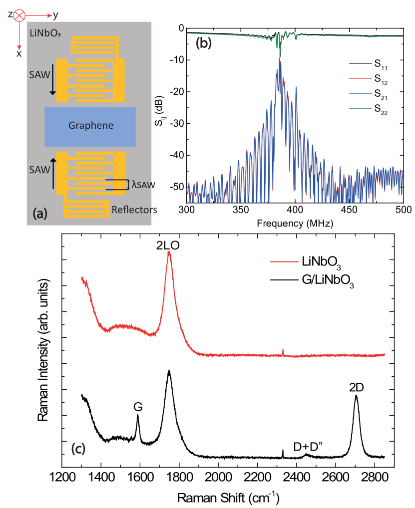
A two-port SAW resonator (SAWR), formed by interdigital transducers (IDTs) and metal reflection gratings, was patterned on rotated Y-cut X-propagating LiNbO by optical lithography followed by lift-off metallization. Single layer graphene (SLG), grown by chemical vapour deposition (CVD), was then transferred to the LiNbO substrate using an automatic transfer system Bosca2016 . The graphene sheet was patterned using an oxygen plasma, leaving a graphene stripe in the region between IDTs, as shown in figure 1(a). The period and aperture of the IDTs were chosen to be 10 m and 100 m, respectively. This value permits to assess the SAW-induced effects by optical microspectroscopy, whereas the selected value is a trade-off providing large SAW power density, negligible diffraction effects in the SAW beam, and good impedance matching. Figure 1(b) shows the power reflection and transmission S parameters of the SAWR, measured with the device already mounted and wire-bonded on the chip used later on for the Raman characterization.
The Raman spectroscopy was performed in backscattering configuration at room temperature using a confocal Horiba LabRam system. The incident 473-nm solid-state laser beam was focused onto a spot of approximately 1 m diameter and 0.8 mW power on the sample surface using a long working distance (50x) objective with a numerical aperture of 0.55. The backscattered light was collected by the same objective, spectrally analyzed by a monochromator with a 1800 grooves/mm dispersion grating and detected using a liquid-nitrogen-cooled charge coupled device (CCD). In order to detect the changes in the Raman spectra induced by the SAW, the amplitude-modulation method described in ref. Iikawa2016 was used. Here, both the RF signal generating the SAW at the IDTs and the excitation laser are chopped with the same modulation frequency (300 Hz) to be either in- or out-of-phase. Spectra were then recorded with the two excitations in phase (i.e. with the sample subjected to both the laser and acoustic excitations; called hereafter SAW ON) and out-of-phase (where the sample is exposed only to the laser; called hereafter SAW OFF) following the alternated sequence SAW OFF - SAW ON - SAW ON - SAW OFF. An acquisition time of 60 s per spectrum was used for each excitation condition and 20 sequences were measured (80 spectra in total). By averaging, respectively, over the 40 SAW ON and 40 SAW OFF cycles, the Raman spectra with () and without () the effects of the SAW were obtained. This method, besides increasing the signal-to-noise ratio due to the integration, minimizes the effects of the systematic fluctuation of the temperature and of the laser power on the Raman signal, allowing us to isolate the strain contribution Iikawa2016 .
III Results and Discussion
The Raman spectra of the bare LiNbO substrate and of the SLG transferred onto it are shown in figure 1(c). LiNbO exhibits a strong Raman peak around 1780 cm-1 which is a two longitudinal optical phonon process Kokanyan15 . The characteristic Raman signature of the SLG, formed by the G and 2D peaks at 1580 and 2700 cm-1 respectively, appears on top of the background provided by the LiNbO substrate. A small D+D” peak is also observed at 2425 cm-1. The intensity ratio and the absence of the characteristic defect (D) peak (at 1350 cm-1) confirms that the graphene is a defect free monolayer. The analysis of the frequency correlation for the G and 2D peaks indicates that the SLG has a residual carrier density of approximately x cm-2 and a native strain, arising from the transfer process and the lattice mismatch with the substrate, of , where the minus sign indicates compressive strain (see appendix A for details).
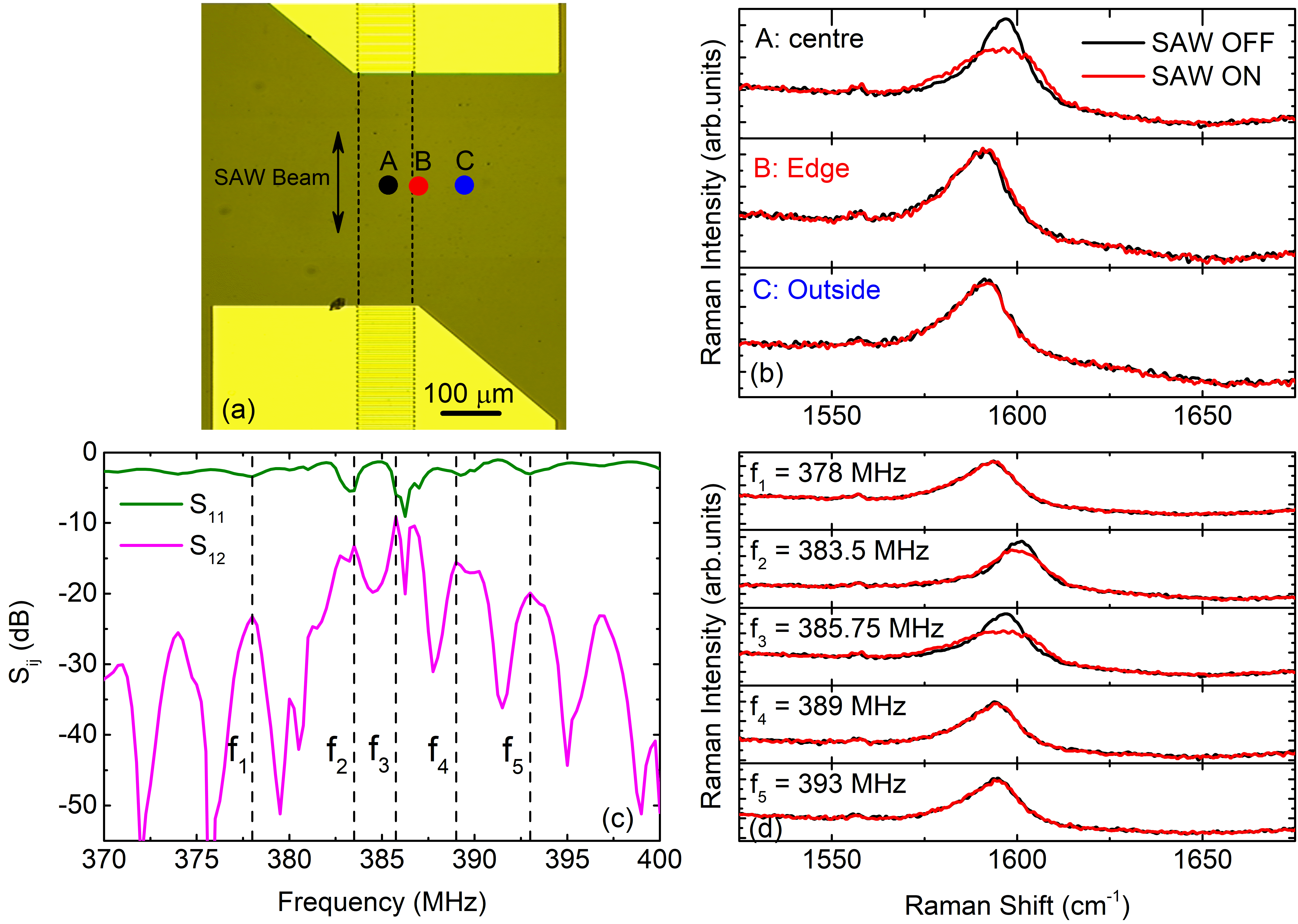
We have investigated the effects of the SAW on the G and 2D Raman bands of the SLG. These bands correspond to the twofold degenerate optical phonons at the point of the Brillouin zone (in-plane C-C stretching mode) and the two optical phonon scattering at the K (and K’) point of the Brillouin zone (in-plane breathing-like mode), respectively. The SAWR produces two counter-propagating travelling SAWs forming a standing SAW pattern with a maximum amplitude at the anti-nodes that is twice as that of a single travelling SAW. The local effect of the SAWs has been first assessed by measuring the Raman spectra at different positions on the sample, marked as A, B, and C on the optical micrograph of the device shown in figure 2(a). The corresponding Raman spectra of the G peak for the SAW ON and SAW OFF cases are depicted in figure 2(b). The intensity modulation and broadening of the peak is only observed within the path of the SAW beam (position A), whereas the Raman spectrum remains unaltered at the edge of and outside that region (positions B and C, respectively). This proves that the modulation observed is solely due to the SAW strain field. In addition, the frequency of the RF signal applied to the IDTs has also been varied across the passband region of the SAWR, as shown in figure 2(c). The dips in (and peaks in ) are due to the different modes of the acoustic resonator. In this case, the maximum phonon modulation is confirmed to peak at a frequency of 385.75 MHz, figure 2(d), where the transmission losses () of the SAW devices are minimum. This modulation fades away rapidly out of the resonance frequency and is negligible for the main side lobes (at 378, 389, and 393 MHz). This also proves that the modulation observed is solely driven by the SAW strain field and rules out any thermal contribution by the laser illumination Papasimakis2015 and the RF dissipation. Furthermore, it demonstrates that the graphene phonons can be modulated dynamically at high frequencies by tuning the RF signal at the IDT. The slight variations in the center wavenumber of the G peak observed in figure 2(b) at different laser positions on the sample are due to the variations in the native strain and residual doping of the graphene (as shown in appendix A), whereas those observed in figure 2(d) for the same laser position and different RF frequencies are produced by small mechanical and thermal drifts. However, these drifts do not affect the differential analysis of the SAW OFF and SAW ON conditions measured at a fixed RF frequency and power, as the above mentioned modulation method cancels out the effects of any systematic fluctuations on the Raman signal (as explained in the experimental section).
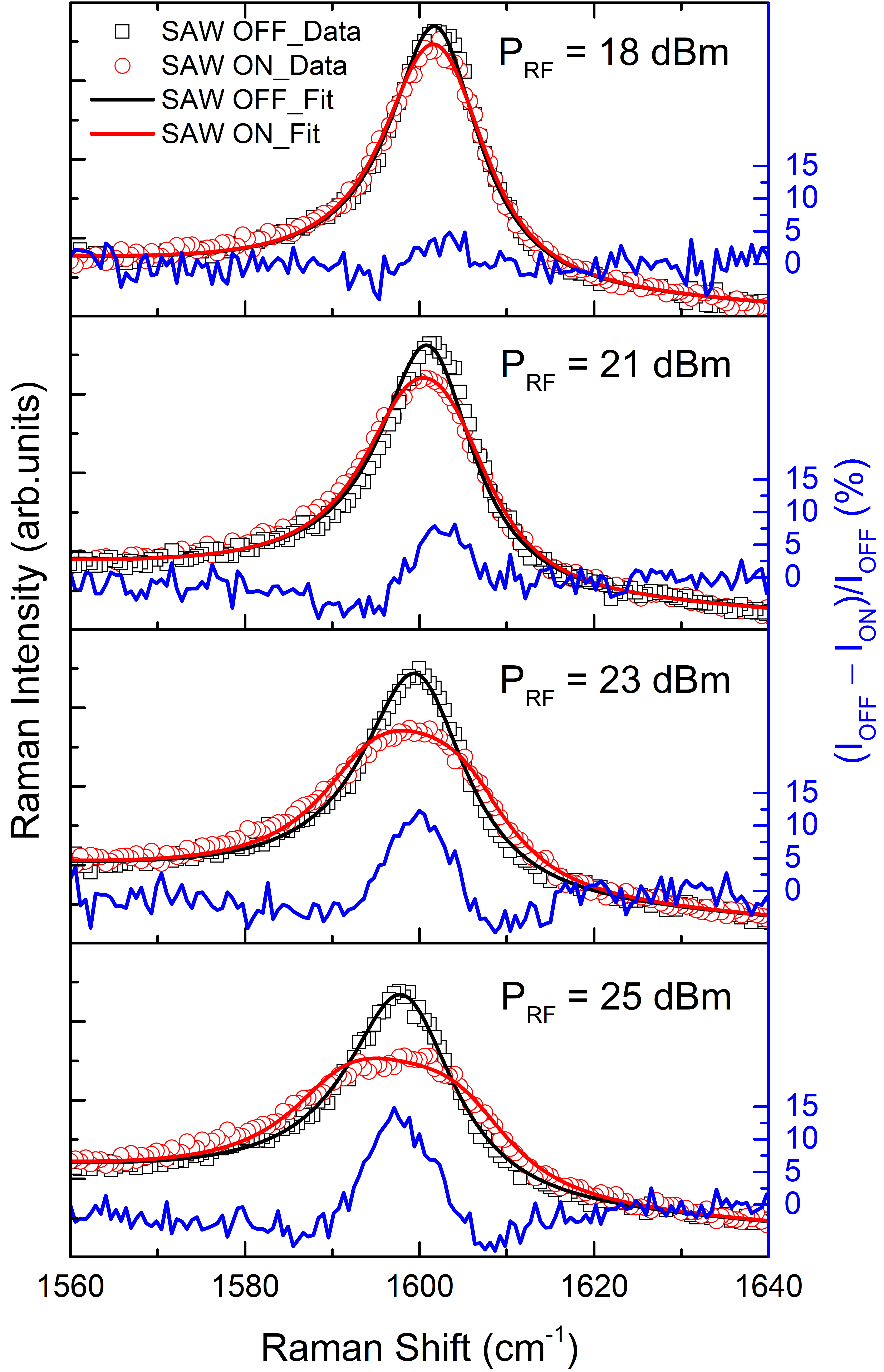
Figure 3 displays the Raman spectra of the G peak for various values for both SAW ON, , and SAW OFF, , cases. The net differential response is also depicted. The spectra have an asymmetric line shape, which arises from the coupling of a discrete phonon spectrum to a continuum of electronic excitations. To account for this line shape, we have fitted the spectra with a Breit-Wigner-Fano (BWF) function Hasdeo2014 , so that reads as follows:
| (1) |
where is the base line, is the slope of straight line used for background removal, is the height of the peak, is the centre of the peak, is the spectral width, and is the asymmetry factor. The condition cancels out the contribution from the continuum of electronic excitations, giving a Lorentzian line shape, which represents a discrete phonon spectrum. The corresponding Raman spectra show an additional line broadening of the G peak and a decrease in for a certain range of values. This broadening in the G peak line shape is interpreted to be caused by the dynamic strain field of the SAW. Thus, the oscillating tensile and compressive cycles of the strain modulate periodically the phonon frequency around its equilibrium value. Since the acquisition time of the Raman spectra is much larger than the SAW period, the phonon oscillation manifests itself as a broadening of the peak line shape and a reduction of its maximum intensity. Both the broadening and the intensity reduction increase with increasing .
The effects of the local SAW strain observed in the graphene G and 2D Raman lines are found to be qualitatively similar to those described in the modulation of the LO phonon Raman line of bulk semiconductor crystals Iikawa2016 . They are also similar to those observed in the photoluminescence of SAW-modulated quantum wells Sogawa2001 and dots Gell2008 ; Pustiowski2015 . In Si, the differential Raman signal is slightly asymmetric Iikawa2016 . The asymmetry was attributed to the scattering events under a SAW involving LO phonons with small wave vectors, which have energies slightly lower than the one for the zone-center mode. This type of asymmetry has not been observed for the graphene G Raman line, thus indicating that these scattering events are not important. Furthermore, the piezoelectric field accompanying the SAW can modulate the carrier concentration in semiconductors leading to broadenings and shifts of the Raman frequency Cerdeira1972 . In the case of SLG, however, the SAW-induced carrier density modulation has been estimated to be of the order of cm-2, which is negligible as compared to the residual carrier density in the material. Nonetheless, the SAW strain modulation observed in graphene is quantitatively much stronger as in the semiconductors due to the combination of the larger Grüneisen parameters of graphene and the more efficient generation of the strain in the 2D layer on a strong piezoelectric substrate, as we will discuss in the next paragraphs.
In order to quantify the modulation of the graphene phonon by the strain field of the standing SAW, we have fitted the spectra with the following integral equation:
| (2) |
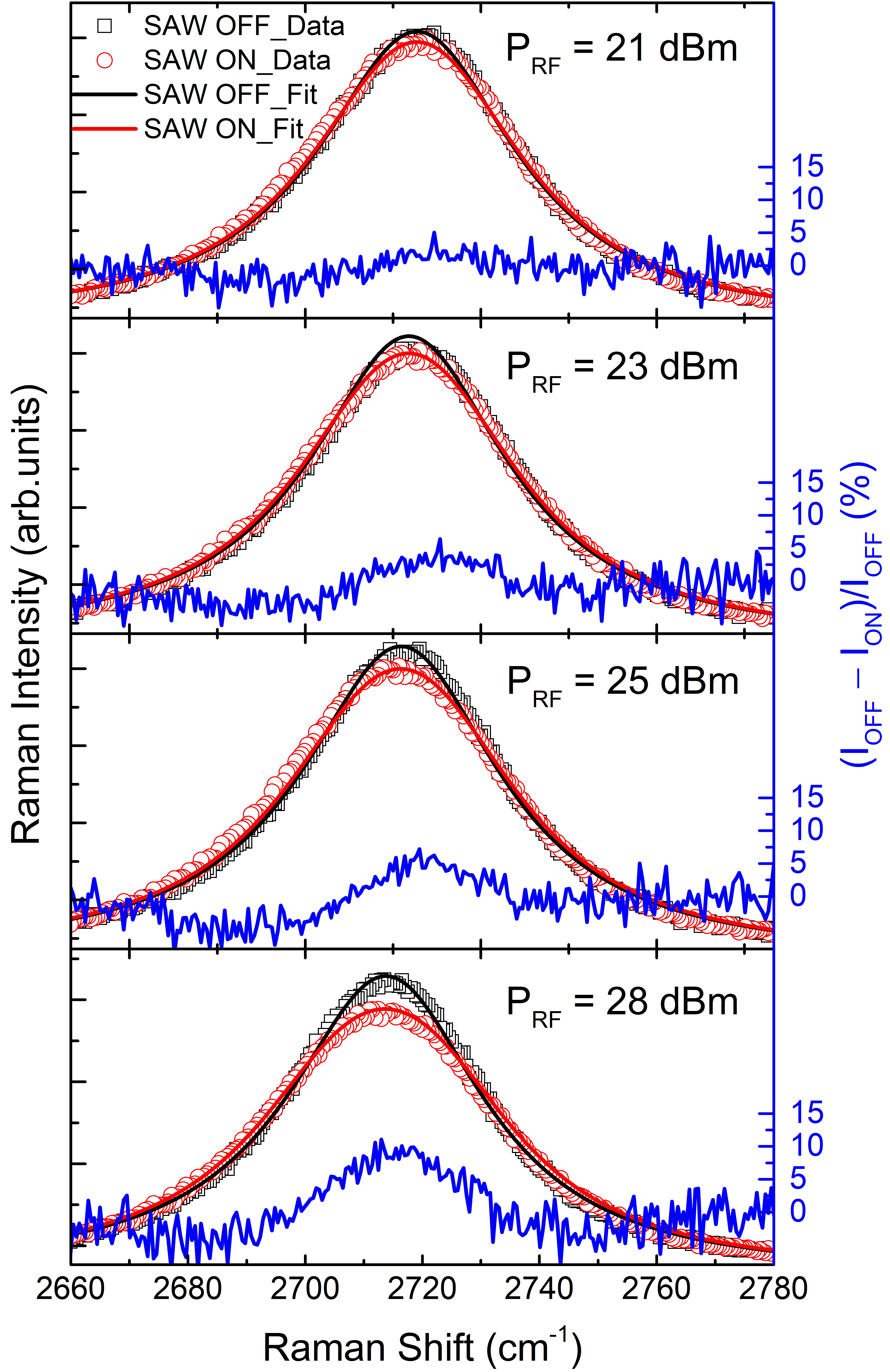
where , , , , , and are the fitting parameters extracted previously from the BWF fitting of for each value of . The amplitude of the SAW-induced phonon frequency modulation is given by , which is the only free parameter in the fitting of . is the absolute value of the SAW-induced modulation, whereas its sign variation within the wave cycle is accounted for by the cosine term. attains a non-zero value only within the SAW beam path, for the SAW resonance frequency, and for a large enough RF power. We have also performed a similar study for the 2D peak, as shown in figure 4. It must be noted that in the case of the 2D peak, is very small, as expected for a band hardly affected by the continuum of electronic excitations. A weaker acoustic modulation is observed for the 2D band as compared to the G band, so that much higher values have been required to obtain a comparable modulation to that of the G band. This is expected to be related to the larger width of the 2D peak that partially hinders the modulation making it less apparent.
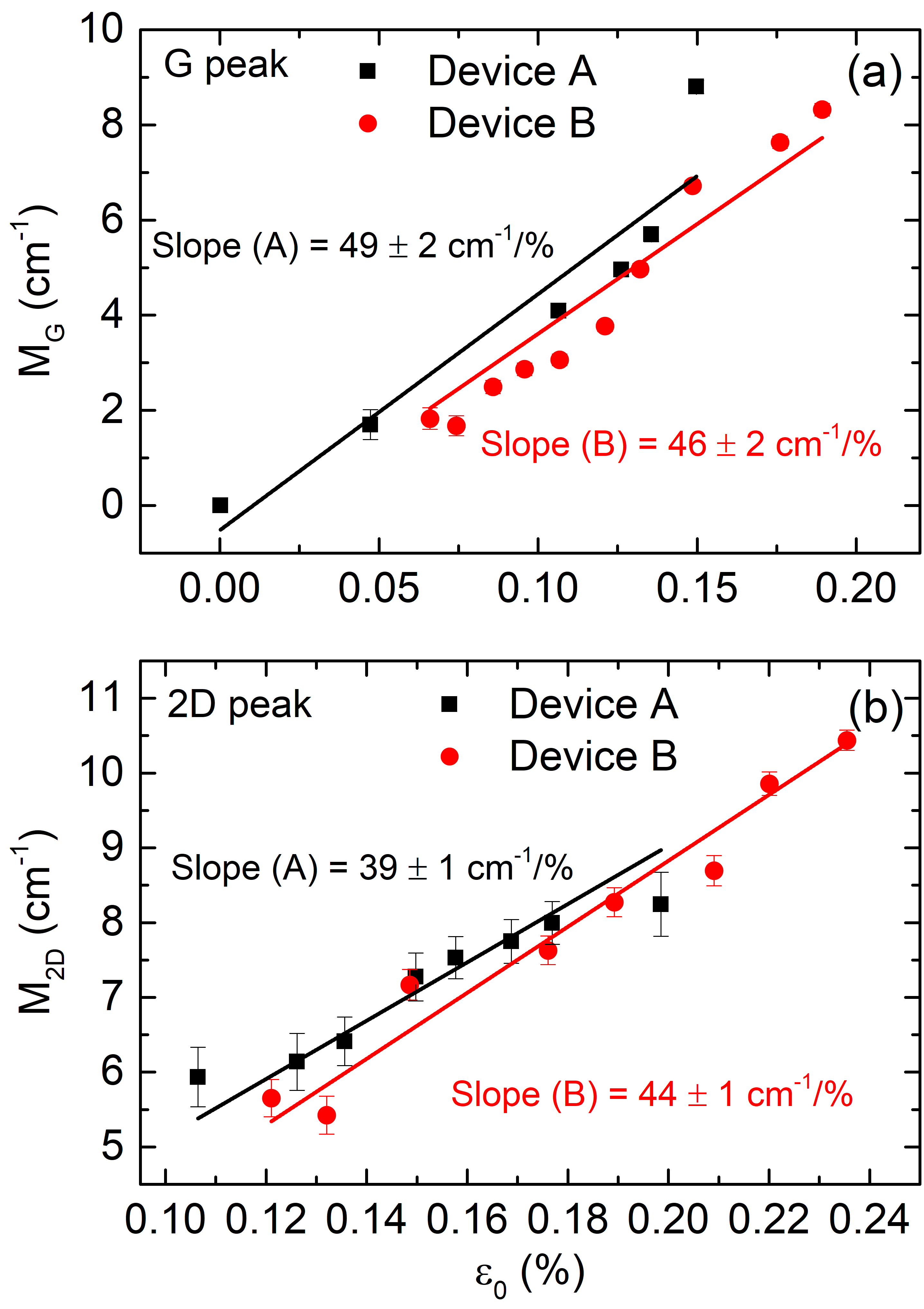
Figures 5(a) and 5(b) display the evolution of the value of for the G, , and 2D, , peaks, respectively, as a function of the absolute value of the hydrostatic strain, , generated by the standing SAW at the surface of the LiNbO3 substrate where the SLG lies. Since the SAW is a Rayleigh mode Rayleigh1885 , i.e. with sagittal polarization, it has only particle displacements along the x and z directions (cf. figure 1(a)). Therefore, the hydrostatic component of the strain field is then . The details of the calculation of as a function of the applied to the IDTs are described in appendix B. Figures 5(a) and 5(b) display the data from two devices (A and B) with identical SAWR but with transferred graphene from two different batches. The linear fittings in figure 5(a) provide a slope value or rate of 49 2 and 46 2 cm for devices A and B, respectively. Similar fittings in figure 5(b) provide a rate of 39 1 and 44 1 cm, respectively, for the same devices. The obtained values are then consistent for both graphene batches used. It has to be noticed that although the strain produced by the SAWR has a quasi-uniaxial character, since is an order of magnitude smaller than , the polycrystalline nature of the CVD SLG used for this study averages out the contribution from several crystal domains, so that the well-known G- Huang2009 ; Mohiuddin2009 ; Frank2010 and 2D-peak Huang2010 ; Frank2011 ; Yoon2011 splitting in (monocrystalline) exfoliated graphene flakes under uniaxial strain is not expected to occur here. Nevertheless, these splittings are foreseen to be induced by the SAWR in SLG monocrystals (CVD or exfoliated).
The rates obtained have allowed us to calculate the respective Grüneisen parameters, , which represent the rate of phonon mode softening (hardening) under tensile (compressive) strain. They are expressed as Note1
| (3) |
where is the centre of the position of the G (2D) peak for the unperturbed (SAW OFF) condition. The values of obtained for devices A and B are 3.1 0.1 and 2.8 0.1, respectively, whereas the values of the corresponding are 1.43 0.04 and 1.63 0.04, respectively.
The Grüneisen parameters are fundamental magnitudes that determine the thermomechanical properties of a material. However, in the case of graphene, there is still a large dispersion of values reported in the literature, with and in the ranges of and , respectively Huang2009 ; Mohiuddin2009 ; Ding2010 ; Metzger2010 ; Cheng2011 . This variation can be attributed to the different type of strain applied, as well as to the quality of the graphene, the substrate used Jiang2018 , and the effective adhesion of the graphene to the substrate Bousige2016 . The smaller value of than of obtained in this study seems to be an artifact related to the less efficient SAW-induced modulation of the 2D band due to its broader nature, as it has been discussed in figure 4. On the other hand, the larger values of obtained in this study, as compared to those reported in the literature, might arise from the large difference in the coefficient of thermal expansion, , of the polymers used in the case of graphene on flexible substrates, such as SU8 in ref. Mohiuddin2009 ( x K-1 Steiner2012 ) or PDMS in ref Huang2009 ( x K-1 Mark2009 ), and of LiNbO ( x K-1 Kim1969 ), as well as due to the dynamic nature of the strain produced by the SAW on the graphene/LiNbO system in contrast to the static strain in the case of the graphene/polymer systems on a flexible substrate.
Most bulk semiconductors have Grüneisen parameters for the zone-center TO and LO (or degenerated LTO) phonons with values around 1 Yu2010 and phonon frequencies in the range of 250-550 cm-1. Therefore, the Raman frequency sensitivity to strain of these materials is expected to be of approximately 5 cm, an order of magnitude smaller than the rates obtained here for graphene modulated by the SAW strain field. In addition, graphene can be easily transferred directly onto a strong piezoelectric substrate providing a large SAW strain amplitude. Conversely, semiconductors are typically weakly or non-piezoelectric, the latter requiring an additional piezoelectric layer on top of them to generate the SAW. Thus, in these cases, the SAW strain amplitude is either small or only a fraction of that produced at the piezoelectric layer reaches the active semiconductor region Pedros2011 . This makes SAWs specially powerful and well-suited tools for the strain modulation of graphene and the development of novel devices thereof.
IV Conclusions
In conclusion, we have investigated the SAW-induced modulation of the phonons of graphene by Raman spectroscopy. We have observed strong effects in both first-order and second-order (or two-phonon) Raman modes, achieving intensity variations of and phonon frequency shifts of around cm-1 when the SAW is applied. The local strain produced by the SAW can be varied by changing the applied RF power and frequency allowing us to dynamically tune the phonon frequency. SAWs might also permit to generate strain along multiple axes and tailor the strain fields. For example, a biaxial strain pattern could be generated by either using orthogonal SAWRs or selecting crystal cuts and propagation directions providing comparable and components Campbell1968 . An adequate design of the in- and out-of-plane strain components of the SAW might also be useful for tailoring gauge fields in graphene Guinea2009 ; Vozmediano2010 . Moreover, the amount of strain generated in the SLG could be enhanced by using focusing IDTs. Furthermore, the piezoelectric field accompanying the SAW in LiNbO leads to a variation of the SLG carrier density of the order of cm-2, which could be used for locally modulating the material near the Dirac point.
The modulation mechanism reported here is not limited to single-layer graphene but can be extended to any other single- or few-layer 2D material, where the physics is specially rich and strain engineering opens a whole range of new possibilities Amorim2016 ; Naumis2017 . Moreover, many 2D materials are themselves piezoelectric Cui2018 , enhancing the capabilities of strain modulation. As an example, the mode has been shown to strongly modify the plasmonic properties of bilayer graphene Low2014 , so that a SAW could be used to tune hybridized plamon-phonon modes for surface-enhanced Raman spectroscopy Marin2017 .
Acknowledgements.
The authors thank Manfred Ramsteiner for helpful discussions and Adolfo del Campo (ICV-CSIC) for his assistance with the preliminary Raman measurements in appendix A. This work has received funding from the European Union’s Horizon 2020 Research and Innovation Programme under Marie Skłodowska-Curie Grant Agreement No 642688, from the Spanish Ministry of Economy and Competitiveness (MINECO) through project DIGRAFEN (ENE2017-88065-C2-1-R), from the Comunidad de Madrid through project NMAT2D-CM (P2018/NMT-4511), and from the Universidad Politécnica de Madrid through project GRAPOL (VJIDOCUPM18JPA). J.P. acknowledges financial support from MINECO (Grant RyC-2015-18968). F.I. acknowledges the Alexander von Humboldt Foundation and the Conselho Nacional de Desenvolvimento Científico e Tecnológico (Nos. 305769/2015-4 and 432882/2018-9) for financial support.Appendix A Graphene native strain
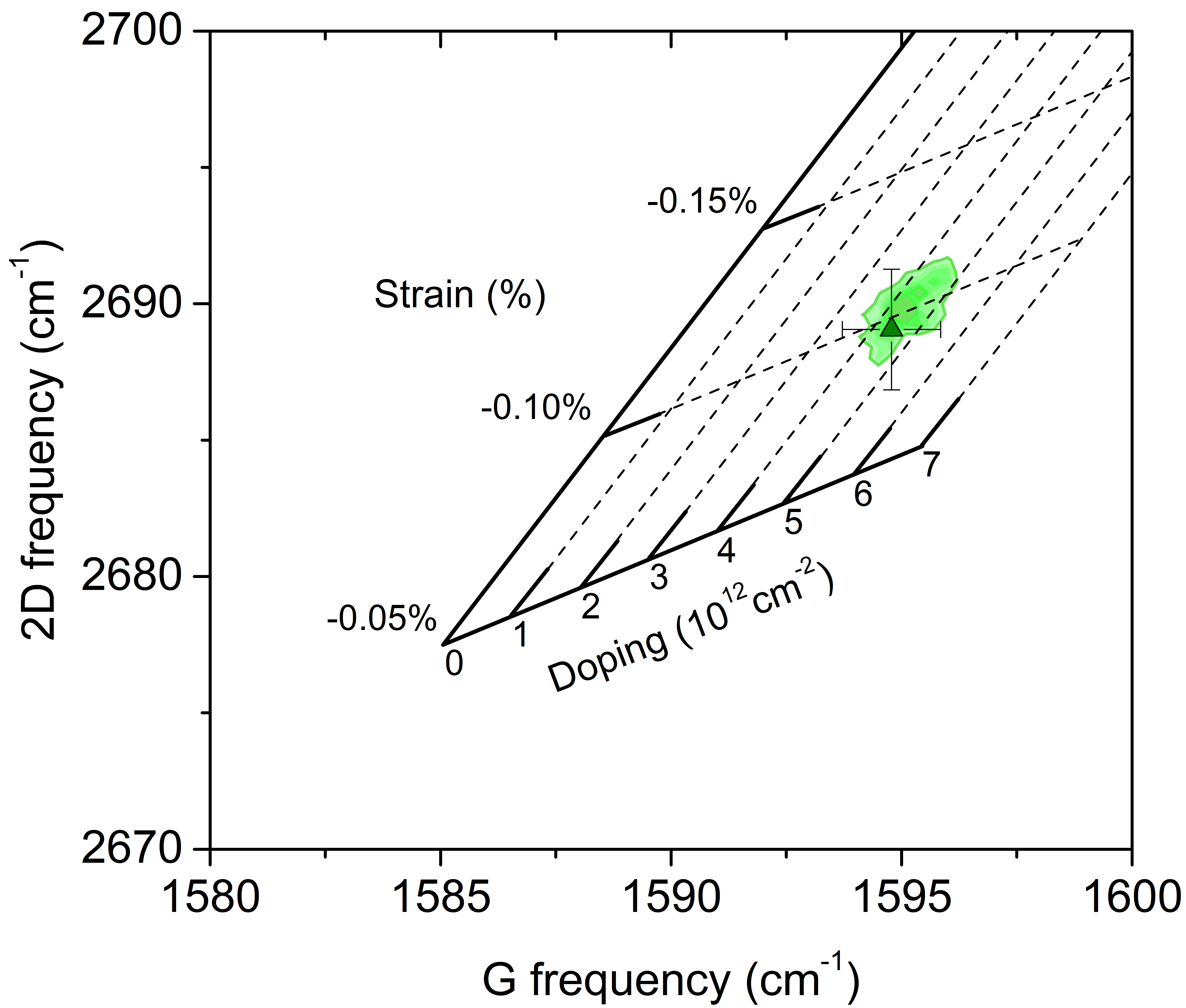
A WITec Alpha 300AR Raman confocal microscope was used for the preliminary Raman spectroscopy mapping of the samples. Raman spectra were obtained in backscattering geometry using a 50x objective lens (numerical aperture of 0.8) in ambient conditions. A 532-nm wavelength laser set to a power of 1 mW was used as excitation source. Typical mapped areas were 80 x 100 m in size, scanned with steps of 4 m.
Figure 6 shows the correlation between the frequencies of the G and 2D peaks in one of these Raman mappings. The larger excitation wavelength used here as compared to the one used for the Raman spectroscopy under a SAW leads to smaller frequencies of the 2D peak Zhao2011 than in previous figures. The diagonal evolution of the data distribution shows a slope value of , which is consistent with graphene under biaxial strain, Metten2014 ; Shin2016 and constant p-type doping, Lee2012b . Using the reported sensitivity values of cm and cm cm-2 Lee2012b , these frequencies are decomposed in a native strain and residual doping-related basis Lee2012b , as shown by the internal set of axes in figure 6.
Appendix B SAW-induced strain vs power density
The output signal from an RF generator was split and amplified, in order to drive each IDT of the SAWR with an RF power (dBm). The SAW power density (power per unit of SAW beam width) generated by each IDT was then calculated using the following relation
| (4) |
The half of the transmission parameter of the SAWR takes into account the electromechanical efficiency of a single IDT and reflection grating.
Rayleigh SAWs have a mixed compressional and shear character, leading to a displacement field vector
| (5) |
where and are the longitudinal and shear vertical components, respectively, and the shear horizontal component is typically zero. In the particular case of rotated Y-cut X-propagating LiNbO, is not zero but approximately 20 times smaller than the other two components, so it has been neglected. Thus, using the Voigt notation, the strain field is written as
| (6) |
where the strain tensor components are given by
| (7) |
and the zero components in equation (B3) appear because . The particle displacements have been calculated by solving numerically the coupled elastic and electromagnetic equations for the LiNbO substrate. This allow us to calculate the strain components and the hydrostatic strain produced by the SAWR in the LiNbO substrate, and transmitted to the graphene layer on top.
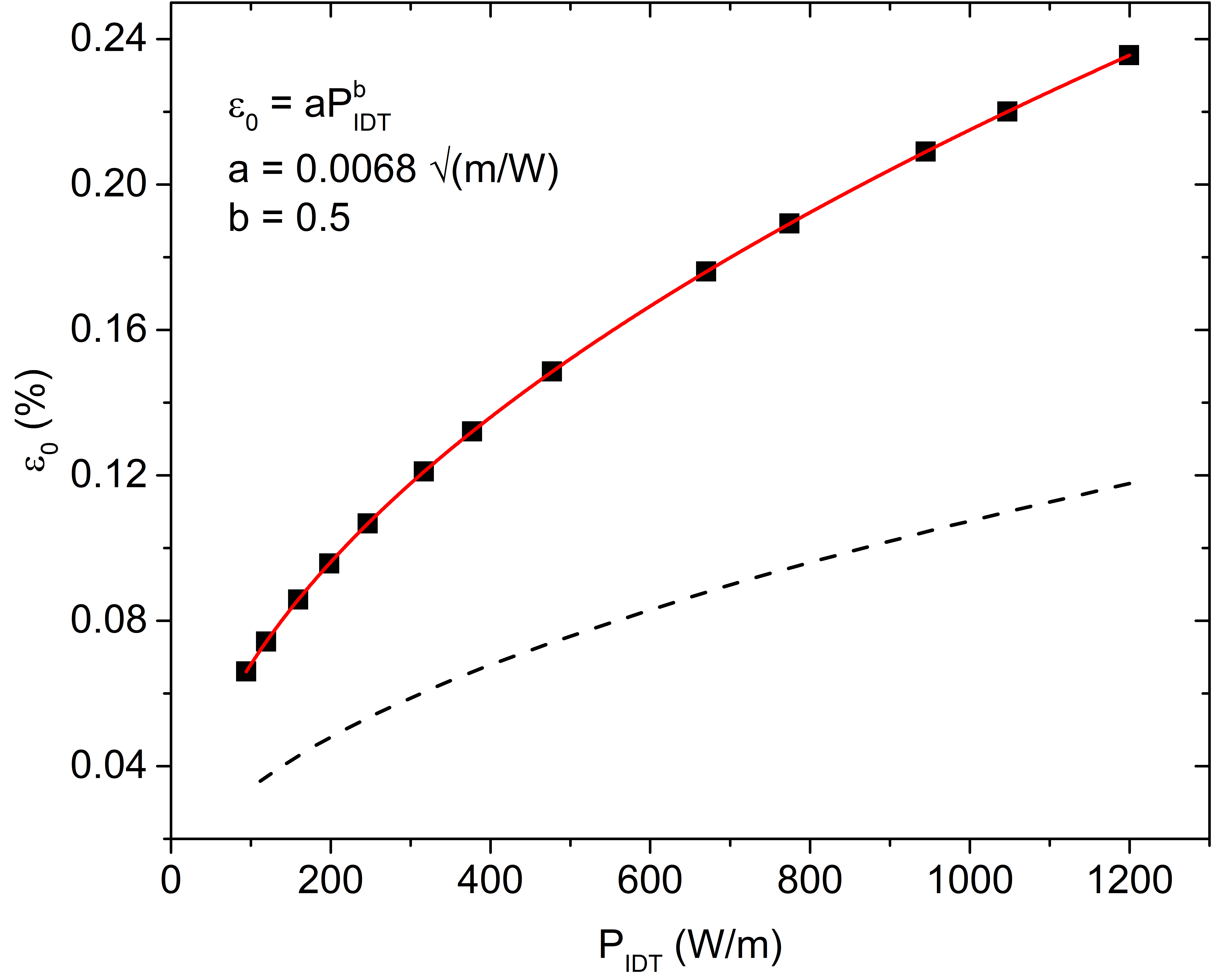
Figure 7 shows the amplitude of as a function of (W/m), where a square root dependence is observed. The maximum strain is achieved at the anti-nodes of the standing wave produced by the SAWR (where both IDTs are excited), which is 2 times larger than that generated by a travelling wave excited by a single IDT. The sign of the strain depends in both cases on the part of the cycle of the wave.
References
- (1) Mayorov A S, Gorbachev R V, Morozov S V, Britnell L, Jalil R, Ponomarenko L A, Blake P, Novoselov K S, Watanabe K, Taniguchi T and Geim A K 2011 Nano Letters 11 2396–2399
- (2) Balandin A A 2011 Nature Materials 10 569–581
- (3) Lee C, Wei X, Kysar J W and Hone J 2008 Science 321 385–388
- (4) Pereira V M, Neto A H C and Peres N M R 2009 Physical Review B 80
- (5) Huang M, Yan H, Chen C, Song D, Heinz T F and Hone J 2009 Proceedings of the National Academy of Sciences 106 7304–7308
- (6) Yoon D, Son Y W and Cheong H 2011 Physical Review Letters 106
- (7) Si C, Liu Z, Duan W and Liu F 2013 Physical Review Letters 111 196802
- (8) Levy N, Burke S A, Meaker K L, Panlasigui M, Zettl A, Guinea F, Neto A H C and Crommie M F 2010 Science 329 544–547
- (9) Guinea F, Katsnelson M I and Geim A K 2009 Nature Physics 6 30–33
- (10) Zhou M, Lu Y, Zhang C and Feng Y P 2010 Applied Physics Letters 97 103109
- (11) Cretu O, Krasheninnikov A V, Rodríguez-Manzo J A, Sun L, Nieminen R M and Banhart F 2010 Physical Review Letters 105
- (12) Ng M L, Balog R, Hornekær L, Preobrajenski A B, Vinogradov N A, Mårtensson N and Schulte K 2010 The Journal of Physical Chemistry C 114 18559–18565
- (13) Wang Z F, Zhang Y and Liu F 2011 Physical Review B 83
- (14) Mohiuddin T M G, Lombardo A, Nair R R, Bonetti A, Savini G, Jalil R, Bonini N, Basko D M, Galiotis C, Marzari N, Novoselov K S, Geim A K and Ferrari A C 2009 Physical Review B 79
- (15) Frank O, Tsoukleri G, Parthenios J, Papagelis K, Riaz I, Jalil R, Novoselov K S and Galiotis C 2010 ACS Nano 4 3131–3138
- (16) Lee J U, Yoon D and Cheong H 2012 Nano Letters 12 4444–4448
- (17) Metten D, Federspiel F m c, Romeo M and Berciaud S 2014 Phys. Rev. Applied 2(5) 054008
- (18) Shin Y, Lozada-Hidalgo M, Sambricio J L, Grigorieva I V, Geim A K and Casiraghi C 2016 Applied Physics Letters 108 221907
- (19) Chen C, Rosenblatt S, Bolotin K I, Kalb W, Kim P, Kymissis I, Stormer H L, Heinz T F and Hone J 2009 Nature Nanotechnology 4 861–867
- (20) Bao W, Myhro K, Zhao Z, Chen Z, Jang W, Jing L, Miao F, Zhang H, Dames C and Lau C N 2012 Nano Letters 12 5470–5474
- (21) Goldsche M, Sonntag J, Khodkov T, Verbiest G J, Reichardt S, Neumann C, Ouaj T, von den Driesch N, Buca D and Stampfer C 2018 Nano Letters 18 1707–1713
- (22) Polyzos I, Bianchi M, Rizzi L, Koukaras E N, Parthenios J, Papagelis K, Sordan R and Galiotis C 2015 Nanoscale 7(30) 13033–13042
- (23) Colangelo F, Pitanti A, Mišeikis V, Coletti C, Pingue P, Pisignano D, Beltram F, Tredicucci A and Roddaro S 2018 2D Materials 5 045032
- (24) Mi H, Mikael S, Liu C C, Seo J H, Gui G, Ma A L, Nealey P F and Ma Z 2015 Applied Physics Letters 107 143107
- (25) Jiang Y, Mao J, Duan J, Lai X, Watanabe K, Taniguchi T and Andrei E Y 2017 Nano Letters 17 2839–2843
- (26) Nemes-Incze P, Kukucska G, Koltai J, Kürti J, Hwang C, Tapasztó L and Biró L P 2017 Scientific Reports 7 3035
- (27) Schiefele J, Pedrós J, Sols F, Calle F and Guinea F 2013 Physical Review Letters 111 237405
- (28) Fandan R, Pedrós J, Schiefele J, Boscá A, Martínez J and Calle F 2018 Journal of Physics D: Applied Physics 51 204004
- (29) Iikawa F, Hernández-Mínguez A, Aharonovich I, Nakhaie S, Liou Y T, Lopes J M J and Santos P V 2019 Applied Physics Letters 114 171104
- (30) Oliva-Leyva M and Naumis G G 2015 Journal of Physics: Condensed Matter 28 025301
- (31) Miseikis V, Cunningham J E, Saeed K, O’Rorke R and Davies A G 2012 Applied Physics Letters 100 133105
- (32) Bandhu L, Lawton L M and Nash G R 2013 Applied Physics Letters 103 133101
- (33) Santos P V, Schumann T, Oliveira M H, Lopes J M J and Riechert H 2013 Applied Physics Letters 102 221907
- (34) Hernández-Mínguez A, Tahraoui A, Lopes J M J and Santos P V 2016 Applied Physics Letters 108 193502
- (35) Liou Y T, Hernández-Mínguez A, Herfort J, Lopes J M J, Tahraoui A and Santos P V 2017 Journal of Physics D: Applied Physics 50 464008
- (36) Preciado E, Schülein F J, Nguyen A E, Barroso D, Isarraraz M, von Son G, Lu I H, Michailow W, Möller B, Klee V, Mann J, Wixforth A, Bartels L and Krenner H J 2015 Nature Communications 6 8593
- (37) Rezk A R, Walia S, Ramanathan R, Nili H, Ou J Z, Bansal V, Friend J R, Bhaskaran M, Yeo L Y and Sriram S 2015 Advanced Optical Materials 3 888–894
- (38) Rezk A R, Carey B, Chrimes A F, Lau D W M, Gibson B C, Zheng C, Fuhrer M S, Yeo L Y and Kalantar-zadeh K 2016 Nano Letters 16 849–855
- (39) Delsing P, Cleland A N, Schuetz M J A, Knörzer J, Giedke G, Cirac J I, Srinivasan K, Wu M, Balram K C, Bäuerle C, Meunier T, Ford C J B, Santos P V, Cerda-Méndez E, Wang H, Krenner H J, Nysten E D S, Weiß M, Nash G R, Thevenard L, Gourdon C, Rovillain P, Marangolo M, Duquesne J Y, Fischerauer G, Ruile W, Reiner A, Paschke B, Denysenko D, Volkmer D, Wixforth A, Bruus H, Wiklund M, Reboud J, Cooper J M, Fu Y, Brugger M S, Rehfeldt F and Westerhausen C 2019 Journal of Physics D: Applied Physics 52 353001
- (40) Iikawa F, Hernández-Mínguez A, Ramsteiner M and Santos P V 2016 Physical Review B 93 195212
- (41) Boscá A, Pedrós J, Martínez J, Palacios T and Calle F 2016 Scientific Reports 6 21676
- (42) Kokanyan N 2015 Study pf photo-electrostrictive effects in photorefractive LiNbO3 probed by polarized Raman spectroscopy Theses Université de Lorraine (Nancy) URL https://hal.archives-ouvertes.fr/tel-01386808
- (43) Papasimakis N, Mailis S, Huang C C, Al-Saab F, Hewak D W, Luo Z and Shen Z X 2015 Applied Physics Letters 106 061904
- (44) Hasdeo E H, Nugraha A R T, Dresselhaus M S and Saito R 2014 Physical Review B 90 245140
- (45) Sogawa T, Santos P V, Zhang S K, Eshlaghi S, Wieck A D and Ploog K H 2001 Phys. Rev. B 63(12) 121307
- (46) Gell J R, Ward M B, Young R J, Stevenson R M, Atkinson P, Anderson D, Jones G A C, Ritchie D A and Shields A J 2008 Applied Physics Letters 93 081115
- (47) Pustiowski J, Müller K, Bichler M, Koblmüller G, Finley J J, Wixforth A and Krenner H J 2015 Applied Physics Letters 106 013107
- (48) Cerdeira F and Cardona M 1972 Phys. Rev. B 5(4) 1440–1454
- (49) Rayleigh L 1885 Proceedings of the London Mathematical Society s1-17 4–11
- (50) Huang M, Yan H, Heinz T F and Hone J 2010 Nano Letters 10 4074–4079
- (51) Frank O, Mohr M, Maultzsch J, Thomsen C, Riaz I, Jalil R, Novoselov K S, Tsoukleri G, Parthenios J, Papagelis K, Kavan L and Galiotis C 2011 ACS Nano 5 2231–2239
- (52) Equation (3) does not include a negative sign as it has been particularized to the case under study where and are absolute values
- (53) Ding F, Ji H, Chen Y, Herklotz A, Dörr K, Mei Y, Rastelli A and Schmidt O G 2010 Nano Letters 10 3453–3458
- (54) Metzger C, Rémi S, Liu M, Kusminskiy S V, Castro Neto A H, Swan A K and Goldberg B B 2010 Nano Letters 10 6–10
- (55) Cheng Y C, Zhu Z Y, Huang G S and Schwingenschlogl U 2011 Physical Review B 83 115449
- (56) Jiang T, Wang Z, Ruan X and Zhu Y 2018 2D Materials 6 015026
- (57) Bousige C, Balima F, Machon D, Pinheiro G S, Torres-Dias A, Nicolle J, Kalita D, Bendiab N, Marty L, Bouchiat V, Montagnac G, Souza Filho A G, Poncharal P and San-Miguel A 2017 Nano Letters 17 21–27
- (58) Steiner H, Keplinger F, Hortschitz W and Stifter M 2012 The non-linear thermal behavior of SU-8 2012 35th International Spring Seminar on Electronics Technology (IEEE) pp 450–454
- (59) Mark J 2009 Polymer Data Handbook (Oxford University Press) ISBN 9780195181012 URL https://books.google.es/books?id=ZCYCPwAACAAJ
- (60) Kim Y S and Smith R T 1969 Journal of Applied Physics 40 4637–4641
- (61) Yu P and Cardona M 2010 Fundamentals of Semiconductors: Physics and Materials Properties Graduate Texts in Physics (Springer Berlin Heidelberg) ISBN 9783642007101 URL https://books.google.es/books?id=5aBuKYBT_hsC
- (62) Pedrós J, García-Gancedo L, Ford C J B, Barnes C H W, Griffiths J P, Jones G A C and Flewitt A J 2011 Journal of Applied Physics 110 103501
- (63) Campbell J J and Jones W R 1968 IEEE Transactions on Sonics and Ultrasonics 15 209–217
- (64) Vozmediano M, Katsnelson M and Guinea F 2010 Physics Reports 496 109 – 148
- (65) Amorim B, Cortijo A, de Juan F, Grushin A, Guinea F, Gutiérrez-Rubio A, Ochoa H, Parente V, Roldán R, San-Jose P, Schiefele J, Sturla M and Vozmediano M 2016 Physics Reports 617 1–54
- (66) Naumis G G, Barraza-Lopez S, Oliva-Leyva M and Terrones H 2017 Reports on Progress in Physics 80 096501
- (67) Cui C, Xue F, Hu W J and Li L J 2018 npj 2D Materials and Applications 2 18
- (68) Low T, Guinea F, Yan H, Xia F and Avouris P 2014 Physical Review Letters 112 116801
- (69) Marin B C, Liu J, Aklile E, Urbina A D, Chiang A S C, Lawrence N, Chen S and Lipomi D J 2017 Nanoscale 9(3) 1292–1298
- (70) Zhao W, Tan P H, Liu J and Ferrari A C 2011 Journal of the American Chemical Society 133 5941–5946
- (71) Lee J E, Ahn G, Shim J, Lee Y S and Ryu S 2012 Nature Communications 3 1024