High-fidelity magnonic gates for surface spin waves
Abstract
We study the propagation of surface spin waves in two wave guides coupled through the dipole-dipole interaction. Essential for the observations made here is the magneto-electric coupling between the spin waves and the effective ferroelectric polarization. This allows an external electric field to act on spin waves and to modify the band gaps of magnonic excitations in individual layers. By an on/off switching of the electric field and/or varying its strength or direction with respect to the equilibrium magnetization, it is possible to permit or ban the propagation of the spin waves in selected waveguide. We propose experimentally feasible nanoscale device operating as a high fidelity surface wave magnonic gate.
Magnetostatic surface waves (MSSWs) Murakami ; Zhang ; WangZhangWang ; Freedman ; Matsumoto ; Iacocca ; Chumak ; Khitun ; Demokritov are key elements for magnonic-based information transfer and processing. For realizing efficient magnonic circuits, reliable coupled MSSW waveguides are essential, as they serve as information channel or signal splitter e1701517 ; Sadovnikov192406 . In the present work, we propose a scheme of an electric-field controlled coupled surface MSSWs. Microscopically, the mechanism is driven by spin-orbit coupling that leads to the emergence of a spin-driven electric polarization coupled to spin-noncollinearity, as discussed for example for Yttrium iron garnet (YIG) Flatte ; Vignale . The mechanism can be viewed as a dynamical Dzyaloshinskii Moriya (DM) coupling, and will be named as such hereafter. Thus, an external electric field that affects the electric polarization steers indirectly the spin order. In this work we will focus on YIG as it has low magnetic damping constant, meaning magnetic losses are negligible on relatively short time scale Serga264002 . The remarkable property of MSSWs is their chiral nature. The chiral character of MSSWs is a purely dynamical effect related to the off-diagonal part of the dynamic dipole-dipole interaction. The dynamically induced chirality leads at least to two exciting phenomena: The non-reciprocal localization of MSSWs propagating perpendicular to the magnetization direction in an in-plane magnetized thin film, and b) the ban on the backscattering, i.e., robust spin-wave modes with the frequency located inside the volume modes (VM) gap, see Mohseni ; Uchida ; Slavin ; Kostylev , and references therein. In the present work, we study the influence of the dynamical DM interaction on the backscattering-immune frequency region in a single MSSW and coupled wave guides which are coupled via the dipole-dipole interaction. We show that the non-reciprocal localization of MSSWs in the coupled wave guides leads to non-reciprocal SW dispersion. Through the DM interaction term, an electric field influences the MSSWs dispersion relations and changes the backscattering-immune frequency region. Furthermore, we study the transfer of MSSWs between two coupled wave guides.
I Theoretical model
For studying the effect of an applied external electric field on the excitation and propagation of MSSWs in a thin YIG film, we start from the Landau-Lifshitz-Gilbert (LLG) equation supplemented by the magnetoelectric coupling term jap073903 ; prb064426
| (1) |
Here , is the saturation magnetization, is the gyromagnetic ratio, N/A2 is the permeability, and is the phenomenological Gilbert damping constant. The effective field consists of the exchange field, the demagnetization field, and the external magnetic field applied along the axis. is the exchange constant. The magnetoelectric coupling term describes the coupling between the spin-driven ferroelectric polarization and applied external electric field . This ferroelectric polarization of YIG in the continuous limit has the form which makes clear the similarity to the Dzyaloshinskii Moriya interaction (DMI). Microscopically, the macroscopic effective electric polarization is magnetically driven. The dynamic spin non-collinearity results in an effective electric polarization . The driving mechanism is effectively a dynamic DMI with a DMI vector , as discussed for example in Ref. [ Vignale ]. Here, , is the exchange coefficient, is the mass of the electron, is the electron charge, is the spin-orbital coupling constant, is the unit vector connecting the magnetic ions. For the parameters MV/cm, 3.4 eV () and m, the effective DMI constant scales with the exchange constant . This estimation is in line with experimental observations in Ref. [ Flatte ]. The demagnetization field in presence of the magnetic dipole-dipole interaction reads
| (2) |
In numerical calculations, we adopt the material parameters for YIG: A/m, J/m, the damping constant and magneto electric coupling pC/m. The magnetic field of the amplitude A/m is applied along the axis (cf. for example Fig.2).
II spin wave dispersion

We utilize Eq. (1) and numerically explore the dispersion relation of MSSWs. Simulations are done for a unit simulation cell covering a single film with a size of . For the numerical integration of the LLG equation (Eq. (1)), we utilize the Dormand-Prince method (RK45) with a fixed time step of 0.5 ps. To calculate the SWs and dispersion curves, at first we let the magnetization to relax to the stationary state. Afterwards the stationary state we consider as the ground state and the SW excitation we add on top of the ground state. To excite SWs in a wide frequency range, we utilize periodic field pulse , with the amplitude T and cutoff frequency GHz, applied locally to the region of the sample . We analyze the fluctuation statistics extracted from each cell during the 200 ns of observation with the time step 20 ps. The frequency resolution of the obtained spectrum is 0.005 GHz. To calculate the SW dispersion relation we use two-dimensional fast Fourier transformation (FFT) . Here, is the i-th cell along axis, and is the total cell number along axis. Simulations done for the cell size of (not shown) lead to identical results. The local equilibrium magnetization is parallel to the axis and MSSW propagates along the axis.
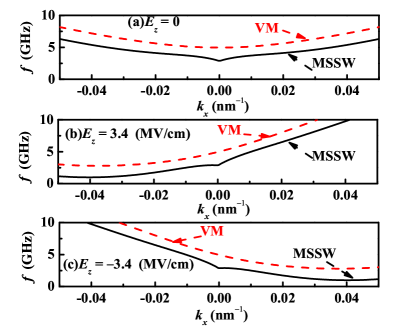
An applied electric field (along the axis) causes in an asymmetry in the spin wave (SW) dispersion relations of MSSWs. The results for the single film is shown in Fig. 1. The positive electric field shifts the dispersion relation towards the lower left side, while the negative shifts it towards the lower right side.
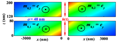
The dispersion relation of MSSW, (see Fig.1) calculated for the single film has a minimum in the point . Profiles of amplitudes of propagating MSSWs are presented in Fig. 2. As we see, the amplitude of the MSSW propagating in the direction has a maximum in the upper surface ( nm) Fig. 2, whereas in contrast amplitude of the MSSW propagating in the reversed direction has a maximum in the lower surface. Reversing of the local magnetization switches the upper/lower surfaces (not shown). Thus localization of the MSSW either in the upper/lower surfaces has a chiral character.
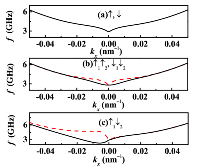
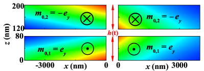
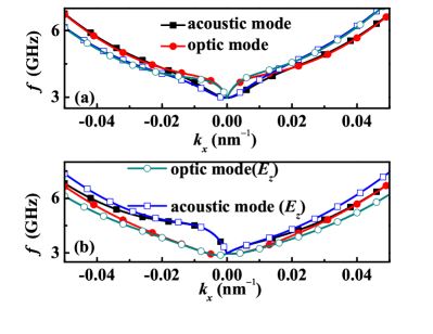
As a next step, we consider two coupled MSSW wave guides and analyze the MSSW dispersion relation for two coupled wave guides. A spacer of the thickness nm is inserted between the two films of the same thickness nm. The dipolar coupling between the films leads to the formation of the ”acoustic” and ”optic” modes prb14950 ; prb144425 . The dispersion relation of the coupled MSSW modes is shown in Fig. 3. When two films have the same equilibrium magnetization (Fig. 3(b)), the dispersion relations have an axial symmetry with respect to the point . In both films, the amplitudes of MSSWs are stronger at upper or lower surfaces, depending on the orientation of the equilibrium magnetization and the propagation direction (Fig. 4). For two films with opposite magnetizations (Fig. 3(c)), the dispersion relations become rather different and asymmetric. The gap between the two MSSW modes is much larger for the MSSWs propagating in the negative direction. Due to opposite magnetizations, the stronger MSSWs are located at different surfaces of the two films, as is shown in Fig. 5. Switching of the magnetization direction either in the case of a single or for the two parallel films has no impact on the MSSW dispersion relations, while in the antiparallel films the dispersion is flipped relative to the point . Hence, the MSSW dispersion relation becomes chiral and nonreciprocal when the films are antiparallel.
III Analytical model
We develop a simple analytical model to understand the MSSW dispersion relations for both single and coupled magnetic films. We apply the constant electric field along the axis , while the static equilibrium magnetization is oriented parallel to the axis . Magnetization vectors in the first and the second films have the form . Here, is the small deviation of magnetization from equilibrium. The wave vector is a sum of the in-plane wave vector and the perpendicular (to the xy plane) wave vector . We insert the magnetization vector into the Eq. (1) and deduce:
| (3) |
Here, enumerates the layers, and the tensor has the form:
| (4) |
Here, for the sake of brevity we introduce the following notations: , , , and . The wave vector , the distance between two wave guides , and is the gap between the wave guides. The dynamic magneto-dipolar interaction is described by the tensore1701517 ; Beleggia ; Verba2012 :
| (5) | ||||
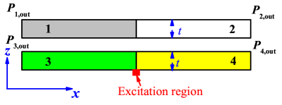
Here, the ”shape amplitude” describes the influence of the finite thickness of the thin film. The pictorial plot of the system is shown in Fig. 6. The SW waveguide consists of two thin magnetic films positioned in the - plane. The thickness of the films is . In direction the films are separated by a spacer with thickness . The distance between the centers of films is . Each film is divided into two regions. The output power of the SW is detected in four ports . The spin wave is excited by an antenna attached to the bottom of the lower film (red region). MSSWs mainly are located near the upper or lower surface (cf. Fig. 2). We introduce thus a localization thickness which is shorter than the real thickness . Due to the dipolar coupling at the boundaries, the thicknesses of the MSSW profiles in different films are identical and pinned together. Therefore, we use the same ansatz to describe the induced nonuniform thickness profiles in both films.
From Eq. (3), we obtain the expressions for the dispersion relations of the MSSW modes. The dispersion relation for the MSSW mode in the isolated film reads
| (6) | ||||
From Eq. (6), we evaluate the difference between frequencies of counter propagating spin waves, . This result is similar to earlier studies KaiDi . The dispersion relation for two coupled layers with the same local magnetization is
| (7) |
If the magnetizations of the layers are opposite to each other, the dispersion relation takes the form
| (8) | ||||
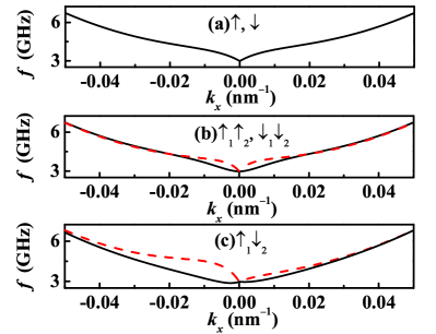
With these analytical expressions we insert the same material parameters, as used for numerics, and calculate the MSSW dispersion relations. For the profile thickness of the fundamental surface wave, we take . To simplify the calculation, for the single film and for parallel films we use . The analytical results for the MSSW dispersion relations plotted in Fig. 7 is in a good agreement with numerical results. In the case of the films with antiparallel ground state magnetization (see Fig. 5), the thickness of the localized MSSW depends on the propagation direction, and the localization thickness is smaller when the MSSW propagates in the direction. Thus, using different for different propagation directions, we obtain distinct MSSW dispersions, as shown in Fig. 7(c). Reversing of the magnetization in both films reverses the localization thickness of the MSSW propagating in the direction, and flips the MSSW dispersion relations. Despite the relative simplicity and approximations, our analytical model and obtained results are in a good agreement with the exact results of the micromagnetic numeric simulation. In both cases, we observe that an applied electric field leads to the asymmetric MSSW dispersion relations, see Figs. 1 and 8. The slight quantitative difference between the numeric and analytical results arises due to the approximations considered in the analytic part.
IV Spin wave propagation in the waveguide with defect
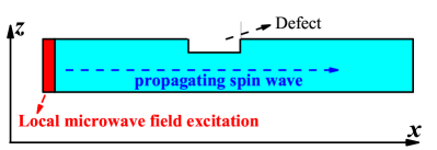

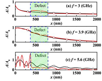
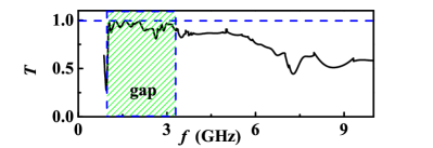
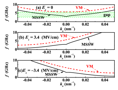
The chiral MSSWs are protected against surface inhomogeneities and defects if the frequency of MSSW matches the band gap Mohseni . The width of the band gap is quantified in terms of the difference between minimum threshold frequencies of VM and MSSW mods, as demonstrated in Fig. 8(a). Our numerical simulations confirm this same result. In the calculation we used the sinc field , T, and GHz applied locally in the left edge of the waveguide (Fig. 9). Thus, spin waves in the frequency interval of GHz are excited. Spin waves with the frequencies lower than the smallest frequency of MSSW mode cannot propagate.
Without electric field (), the lower frequency bound of MSSW is about 2.8 GHz see Fig. 1. An embedded defect at the surface of the film induces scattering of the spin wave. The scattering process sharply depends on the frequency of the spin wave . Comparing the amplitudes of the spin waves in the waveguide with () and without () the embedded defect, we numerically evaluate the transmission ratio and quantify the transmission coefficient of spin waves to describe the scattering process (Fig. 10). In the gap, is about 1, indicating that the bulk of MSSWs can transmit through the defect without reflection, i.e backscattering is not permitted. The transmission becomes much smaller than 1 outside the gap, due to the strong reflection from the defect. We also compare the spatial distributions of and in Fig. 11. In the absence of the embedded defect, the amplitude decays in the direction. In addition, at GHz (beyond the gap), due to the interaction between two SWs with different wave-vectors (MSSW and VM), the amplitude is not uniform and oscillates with . After embedding the defect, we see a clear signature of the reflection process and the scattering from defects for GHz (), whereas for GHz (), the spin wave entirely transmits through the defect. Our results are in a good agreement with the Ref. [ Mohseni ].
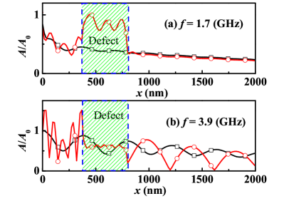
Applying an electric field shifts the gap down and thus decreases the frequency interval with , as shown in Fig. 12. In the frequency interval from GHz, the frequency of the MSSW matches the band gap, and therefore MSSW can transmit through the defect entirely without reflection (as demonstrated by the amplitude for the frequency () in Fig. 13(a)). Outside the band gap, the reflection of the spin wave at the defect becomes significant (Fig. 12). The reflection, at GHz () is shown in Fig. 13(b).
V SW transfer between two coupled films: The role of the electric field
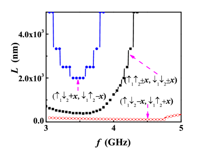
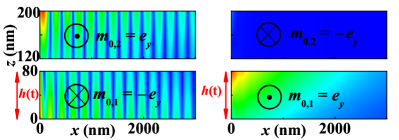
We consider the dynamics of simultaneously excited two propagating SW modes. The wave guides are coupled through the dipole-dipole interaction. The dipole-dipole coupling splits the waveguide modes into the symmetric (acoustic) and asymmetric (optical) mods. The acoustic and optical modes may interact and exchange energy. The transfer of the energy takes place on the characteristic length scale termed as ”coupling length” e1701517 . The coupling length characterizes the propagation length of the SW excitation in the first waveguide, before transferring the energy to the second waveguide, i.e. ”mean free path” of the SW. The is the difference between the wave vectors of the acoustic and the optical modes at the same frequency. The simulated value of the coupling length depends on the frequency of the propagating wave, see Fig. 14. Our results show that the coupling length and the energy transfer process can be controlled through two factors: the direction of the equilibrium magnetization and the direction of propagation of SWs. For example, for GHz, for ( and ) is much larger than nm for ( and ). The energy transfer can be switched on and off via switching the magnetization directions. The propagating SW excited in the lower film (Fig. 15), is effectively decoupled from the upper film . The energy transmission is switched as nm after reversing the magnetization.
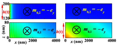
Besides, an electric field shifts the SW dispersion relation in the coupled films, and this fact is important for controlling the transmission properties of the SWs. The electric field applied only to a single film shifts selectively the dispersion relation solely in this layer (similar to Fig. 1). Therefore, the SW for a frequency lower than 3 GHz can propagate in the selected film, while propagation in the second layer is forbidden. To illustrate this statement, we apply the microwave field of the frequency GHz, to the bottom or top layer in the vicinity of the region and excite the SW. The constant electric field we apply to the bottom layer only. SW propagates in the bottom layer, while propagation in the top layer is restricted, see Fig. 16. Typically, the chirality leads to a breaking of the inversion symmetry. The dynamically imposed chirality shows the same features. The effect we observed for SWs is somewhat similar to the phenomenon observed in the context of non-hermetian optics nat192 (in fact, for narrow waveguides in the paraxial approximation our models can be mapped to the PT-symmetric model used for the coupled photonic waveguides nat192 ), and allows us to switch on/off the propagation of MSSWs in the selected layer.
VI The designing of the spin wave directional coupler
The functionality of the reconfigurable nanoscale spin wave directional coupler depends on the structure of the band gap (efficiently controlled through the electric field) and the direction of the ground state equilibrium magnetization. The direction of the magnetization can be switched via the external magnetic field or the current-induced spin-orbit torque (SOT). The SOT has in addition certain advantages, see Ref. [ Scientific Reports ] for more details.
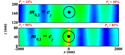
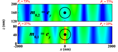
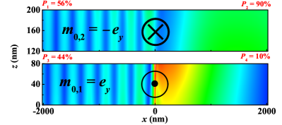
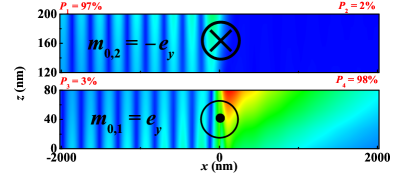
Here, we propose a reconfigurable directional coupler utilizing SOT for controlling the direction of magnetization: In parallel coupled films, the dispersion relation, as well as coupling length , are the same for the opposite propagation directions of MSSWs. Thus and reach their maxima or minima synchronous at the same moment of time, as demonstrated in Figs. 17 and 18. After switching the magnetization distribution to the anti-parallel direction, the dispersion relation and becomes asymmetric (Fig. 14), and the large difference between left side output and right side output develops, as is demonstrated in Figs. 19 and 20.
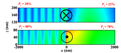
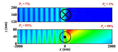
The external electric field applied to both films shifts the SW dispersion (see Eqs. (7) and (8)), as demonstrated in Fig. 21. Shifting of the dispersion relations changes the value of , leading to the electrically reconfigurable directional coupler . In Figs. 22 and 23 the output is plotted for the electric field MV/cm, whereas in (Figs. 19 and 20) the electric field is zero, and the value of the output is different.
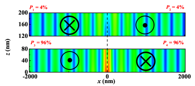
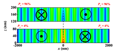
We note that the magnetization moments in four different regions (Fig. 6) near the output terminals accept the selective individual control, and this is a definite advantage of the functionality of proposed directional coupler. The control is achievable through the current-induced spin-orbit torque and external magnetic field. In Figs. 24 and 25, we show amplitudes of propagating MSSWs in the anti-parallel films with magnetic domain walls located near the center (). SWs propagating in and directions share the same chirality, and thus we obtain symmetric outputs in anti-parallel films, i.e. and .
For an experimental realization we suggest the following schemes for exciting spin waves with wave-vectors up to nm-1. The emergent net ferroelectric polarization coupled (through the magneto-electric coupling) to the external electric field mimics an effective DM term. Thus, the applied nonuniform electric field is equivalent to the nonuniform DM term and leads to a particular type of the torque termed as inhomogeneous electric torque prb064426 . The expression of the inhomogeneous electric torque is similar to the spin-transfer torque . The vector , points to the direction of the electric field, and the electric field gradient determines the coefficient . Therefore, the applied oscillating inhomogeneous electric field and , with at , leads to an oscillating electric torque, excites the magnetization oscillation at and short-wavelength spin waves. The inhomogeneous electric field can be realized by a combination of uniform electric field and a normal metallic cap layer shielding the region . Besides, via the microwave magnetic field from antennas, one can excite large wavelength spin-waves in the region of a large internal effective magnetic field. The wavelength of the wave becomes smaller as soon as the wave crosses the region of the lower internal effective magnetic field. This method was proposed in Ref. [ KostylevDemidov ]. The different effective magnetic fields can be achieved by changing the geometry of the sample, attaching an exchange bias layer to the part of the magnetic layer, or covering the waveguide by the superconducting material (at the temperature below ).
VII Switching of the static magnetization
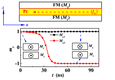
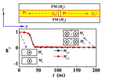
For practical realization, we suggest using the spin Hall torque for switching the magnetization in coupled films. As is shown in Fig. 26, the Pt spacer with electronic current in direction generates the spin Hall torques . Here, represents the polarization direction, the coefficient is proportional to the electronic current density in Pt, and and correspond to the bottom and the top layers. Also, we consider a small anisotropy constant J/m3 (axis is along ) in both films. Torques have opposite directions in layers and tends to be aligned along the direction. For A/m, switching of magnetizations induced by the spin Hall torque is shown in Fig. 26. In dozens of nanoseconds the state with parallel magnetizations is switched to the anti-parallel state. After turning off the electric current, the system stays in anti-parallel state. By applying a strong enough uniform magnetic field, one can easily switch the state back to the parallel state.
To generate the desired configuration of magnetic domain walls, we use the spin Hall torque, as demonstrated in Fig. 27. Two Pt layers with opposite electric currents generate opposite torques in two edges of the single film. The torques are also opposite in different films. The spin Hall torques with A/m generate the particular structure of domain wall as studied here, e.g. in Fig. 27. The magnetic domain walls are stable after the electric current is turned off.
VIII Conclusions
Magnetostatic surface waves and surface waves propagating in coupled parallel wave guides are prototype examples of the simplest integrated magnonic circuits. The surface waves coupled through the dipole-dipole interaction periodically exchange energy. For a high fidelity of magnonic gates, the process of energy exchange should be well under control. In the present work, we proposed a particular type of surface wave magnonic gate controlled through an external static electric field. By varying the strength or direction of electric field, it is possible to shift selectively the chiral MSSW dispersion relation in coupled waveguide. The fact is used for manipulation of the propagation and transfer of the SWs in waveguides. Combining this effect, we propose an electrically reconfigurable nanoscale spin wave directional coupler, and its outputs can be selectively changed via controlling the electric field or magnetization. The adopted electric field is easy to realize and control, which is helpful for designing high fidelity surface wave magnonic devices.
IX Acknowledgment
We acknowledge financial support from the National Natural Science Foundation of China (No. 11704415, 11674400, 11374373), DFG through SFB 762 and SFB TRR227, and the Natural Science Foundation of Hunan Province of China (No. 2018JJ3629).
References
- (1) R. Shindou, R. Matsumoto, S. Murakami, and J. I. Ohe, Topological chiral magnonic edge mode in a magnonic crystal, Phys. Rev. B 87, 174427 (2013).
- (2) L. Zhang, J. Ren, J. S. Wang, and B. Li, Topological magnon insulator in insulating ferromagnet, Phys. Rev. B 87, 144101 (2013).
- (3) X. S. Wang, H. W. Zhang, and X. R. Wang, Topological Magnonics: A Paradigm for Spin-Wave Manipulation and Device Design, Phys. Rev. Appl. 9, 024029 (2018).
- (4) R. Chisnell, J. S. Helton, D. E. Freedman, D. K. Singh, R. I. Bewley, D. G. Nocera, and Y. S. Lee, Topological Magnon Bands in a Kagome Lattice Ferromagnet, Phys. Rev. Lett. 115, 147201 (2015).
- (5) R. Shindou, J. I. Ohe, R. Matsumoto, S. Murakami, and E. Saitoh, Chiral spin-wave edge modes in dipolar magnetic thin films, Phys. Rev. B 87, 174402 (2013).
- (6) E. Iacocca and O. Heinonen, Topologically Nontrivial Magnon Bands in Artificial Square Spin Ices with Dzyaloshinskii-Moriya Interaction, Phys. Rev. Appl. 8, 034015 (2017).
- (7) A. V. Chumak, V. I. Vasyuchka, A. A. Serga, and B. Hillebrands, Magnon spintronics, Nat. Phys. 11, 453 (2015).
- (8) K. Alexander, B. Mingqiang, and L. W. Kang, Magnonic logic circuits, J. Phys. D: Appl. Phys. 43, 264005 (2010).
- (9) S. Urazhdin, V. E. Demidov, H. Ulrichs, T. Kendziorczyk, T. Kuhn, J. Leuthold, G. Wilde, and S. O. Demokritov, Nanomagnonic devices based on the spin-transfer torque, Nat. Nanotechnol. 9, 509 (2014).
- (10) Q. Wang, P. Pirro, R. Verba, A. Slavin, B. Hillebrands, and A. V. Chumak, Reconfigurable nanoscale spin-wave directional coupler, Sci. Adv. 4, e1701517 (2018).
- (11) A. V. Sadovnikov, C. S. Davies, S. V. Grishin, V. V. Kruglyak, D. V. Romanenko, Y. P. Sharaevskii, and S. A. Nikitov, Magnonic beam splitter: The building block of parallel magnonic circuitry, Appl. Phys. Lett. 106, 192406 (2015).
- (12) X. Zhang, T. Liu, M. E. Flatte, and H. X. Tang, Electric-Field Coupling to Spin Waves in a Centrosymmetric Ferrite, Phys. Rev. Lett. 113, 037202 (2014).
- (13) T. Liu and G. Vignale, Electric Control of Spin Currents and Spin-Wave Logic, Phys. Rev. Lett. 106, 247203 (2011).
- (14) A. A. Serga, A. V. Chumak, and B. Hillebrands, YIG magnonics, J. Phys. D: Appl. Phys. 43, 264002 (2010).
- (15) M. Mohseni, R. Verba, T. Bracher, Q. Wang, D. A. Bozhko, B. Hillebrands, and P. Pirro, Backscattering-Immune Chiral Spin-Wave Modes for Protected Magnon Transport at the Nano-Scale, arXiv:1806.01554.
- (16) T. An, V. I. Vasyuchka, K. Uchida, A. V. Chumak, K. Yamaguchi, K. Harii, J. Ohe, M. B. Jungfleisch, Y. Kajiwara, H. Adachi, B. Hillebrands, S. Maekawa, and E. Saitoh, Unidirectional spin-wave heat conveyer, Nat. Mater. 12, 549 (2013).
- (17) I. Lisenkov, V. Tyberkevych, A. Slavin, P. Bondarenko, B. A. Ivanov, E. Bankowski, T. Meitzler, and S. Nikitov, Spin-wave edge modes in finite arrays of dipolarly coupled magnetic nanopillars, Phys. Rev. B 90, 104417 (2014).
- (18) M. Kostylev, Non-reciprocity of dipole-exchange spin waves in thin ferromagnetic films, J. Appl. Phys. 113, 053907 (2013).
- (19) X.-g. Wang, L. Chotorlishvili, G.-h. Guo, C. L. Jia, and J. Berakdar, Thermally assisted skyrmion drag in a nonuniform electric field, Phys. Rev. B 99, 064426 (2019).
- (20) X.-g. Wang, L. Chotorlishvili, G.-h. Guo, and J. Berakdar, Electric field controlled spin waveguide phase shifter in YIG, J. Appl. Phys. 124, 073903 (2018).
- (21) R. Zivieri, L. Giovannini, and F. Nizzoli, Acoustical and optical spin modes of multilayers with ferromagnetic and antiferromagnetic coupling, Phys. Rev. B 62, 14950 (2000).
- (22) A. Konovalenko, E. Lindgren, S. S. Cherepov, V. Korenivski, and D. C. Worledge, Spin dynamics of two-coupled nanomagnets in spin-flop tunnel junctions, Phys. Rev. B 80, 144425 (2009).
- (23) M. Beleggia, S. Tandon, Y. Zhu, and M. De Graef, On the magnetostatic interactions between nanoparticles of arbitrary shape, J. Magn. Magn. Mater. 278, 270 (2004).
- (24) R. Verba, G. Melkov, V. Tiberkevich, and A. Slavin, Collective spin-wave excitations in a two-dimensional array of coupled magnetic nanodots, Phys. Rev. B 85, 014427 (2012).
- (25) K. Di, V. L. Zhang, H. S. Lim, S. C. Ng, M. H. Kuok, X. Qiu, and H. Yang, Asymmetric spin-wave dispersion due to Dzyaloshinskii-Moriya interaction in an ultrathin Pt/CoFeB film, Appl. Phys. Lett. 106, 052403 (2015); J.-H. Moon, S.-M. Seo, K.-J. Lee, K.-W. Kim, J. Ryu, H.-W. Lee, R. D. McMichael, and M. D. Stiles, Spin-wave propagation in the presence of interfacial Dzyaloshinskii-Moriya interaction, Phys. Rev. B 88, 184404 (2013).
- (26) C. E. Rüter, K. G. Makris, R. El-Ganainy, D. N. Christodoulides, M. Segev, and D. Kip, Observation of parity–time symmetry in optics, Nat. Phys. 6, 192 (2010).
- (27) Z. Ren, S. Liu, L. Jin, T. Wen, Y. Liao, X. Tang, H. Zhang, and Z. Zhong, Reconfigurable nanoscale spin-wave directional coupler using spin-orbit torque, Sci. Rep. 9, 7093 (2019); L. Chotorlishvili, Z. Toklikishvili, X. G. Wang, V. K. Dugaev, J. Barnas, and J. Berakdar, Influence of spin-orbit and spin-Hall effects on the spin-Seebeck current beyond linear response: A Fokker-Planck approach, Phys. Rev. B 99, 024410 (2019).
- (28) V. E. Demidov, M. P. Kostylev, K. Rott, J. Münchenberger, G. Reiss, and S. O. Demokritov, Excitation of short-wavelength spin waves in magnonic waveguides, Appl. Phys. Lett. 99, 082507 (2011).