Tunable Electronic Structure in Gallium Chalcogenide van der Waals Compounds
Abstract
Transition metal monochalcogenides comprise a class of two-dimensional materials with electronic band gaps that are highly sensitive to material thickness and chemical composition. Here, we explore the tunability of the electronic excitation spectrum in GaSe using angle-resolved photoemission spectroscopy. The electronic structure of the material is modified by in-situ potassium deposition as well as by forming GaSxSe1-x alloy compounds. We find that potassium-dosed samples exhibit a substantial change of the dispersion around the valence band maximum (VBM). The observed band dispersion resembles that of a single tetralayer and is consistent with a transition from the direct gap character of the bulk to the indirect gap character expected for monolayer GaSe. Upon alloying with sulfur, we observe a phase transition from AB to stacking. Alloying also results in a rigid energy shift of the VBM towards higher binding energies which correlates with a blue shift in the luminescence. The increase of the band gap upon sulfur alloying does not appear to change the dispersion or character of the VBM appreciably, implying that it is possible to engineer the gap of these materials while maintaining their salient electronic properties.
I Introduction
The ability to isolate monolayers and study their physical properties has led to a resurgence of interest in layered van der Waals (VDW) materials as two-dimensional systems. Transition-metal chalcogenides belong to this class of materials and demonstrate unique thermoelectric, photonic and electronic propertiesWasala et al. (2017). The composition, phase, and crystal structure of these materials can be tuned to display a wide range of electronic phases including metallicNovoselov et al. (2004); Feng et al. (2011), semiconductingMak et al. (2010); Splendiani et al. (2010); Watanabe et al. (2004), superconductingGuillamón et al. (2008); Navarro-Moratalla et al. (2016); Ugeda et al. (2015) and charge-density waveLiu et al. (2018); Xi et al. (2015); Ugeda et al. (2015), inspiring utilization in a wide range of applications including electronic devices, sensors, and quantum devicesChoi et al. (2017).
In their bulk form, monochalcogenides of Ga and In, such as GaSe, InSe, and GaS are van der Waals compounds. Gallium chalcogenides (GCs) are direct bandgap semiconductors that can be mechanically exfoliated from a bulk parent crystal. Their properties are highly sensitive to material thickness, chemical composition, and crystalline structureRybkovskiy et al. (2014); Cai et al. (2016); Robertson (2001). Bulk GaSe and GaS have direct band gaps of 2.10 eV and 3.05 eV, respectively, and transition to indirect gaps when the number of layers is reducedLei et al. (2013); Ben Aziza et al. (2017). Monolayer field effect devices maintain mobilities on the order of of 0.1 cm2V-1s-1, on/off ratios of - as well as quantum efficiencies that exceed those of graphene by several orders of magnitude when implemented in a device architectureHu et al. (2012); Zhou et al. (2014); Late et al. (2012).
Alloys with mixed chalcogen content, GaSxSe1-x, allow for control of the bandgap, allowing engineering of the optical absorption and photoluminescence (PL)Serizawa et al. (1980); Jung et al. (2015). Interlayer coupling, defects, doping, and interaction with an underlying substrate may further modify the electronic structure of the GCs, as observed in exfoliated flakes of GaSe and GaTe on SiO2 and grapheneChen et al. (2015); Del Pozo-Zamudio et al. (2015); Kim et al. (2016) and epitaxially grown GaSe flakes on grapheneBen Aziza et al. (2017, 2016); Li et al. (2015).
In this communication, we illustrate how the crystalline and electronic properties of GC materials are affected by changes in chemical composition, doping, and reduced dimensionality using high resolution scanning transmission electron microscopy (HRSTEM), angle-resolved photoemission spectroscopy (ARPES), and PL.
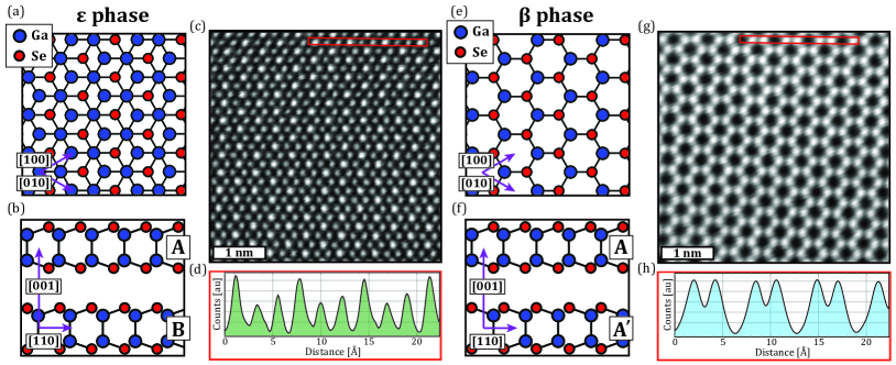
HRSTEM reveals that GaSe tetralayers stack in the AB sequence ( phase) while sulfur alloys and GaS stack almost exclusively in the AA′ sequence ( phase). The complete electronic structure of AB-stacked GaSe is determined using ARPES, allowing us to directly extract the band dispersion along high symmetry directions and determine valence band (VB) extrema and effective masses. We illustrate how the full energy-momentum-resolved quasiparticle band structure of the GCs is modulated when the chemical composition and/or interaction between layers is changed. We explore the influence of potassium deposition on the band structure, finding it only causes a slight energy shift of the VBs and does not lead to degenerate doping which would enable ARPES visualization of the conduction band. However, potassium dosing does lead to a significant change of the dispersion around the top of the VB, implying a strong modification at the surface GaSe tetralayer compared to the bulk. Finally, we explore the effect of sulfur alloying on the band structure. We find that increasing sulfur content produces a rigid VB shift and results in a corresponding blue shift in the PL, suggesting that alloying is a viable method for tuning GC optical properties.
II Experimental
We study pure GaSe and GaS as well as three alloy compositions spanning the entire compositional range of GaSxSe1-x alloys. Crystals are grown using the modified Bridgman-Stockbarger methodNi et al. (2013). Briefly, stoichiometric amounts of Ga, S, and Se powder are weighed and mixed in sealed quartz ampoules to achieve the desired alloying ratio. The Ampoules are then heated in a zone furnace at 970 ∘C for two weeks to grow single crystals 2-8 mm in diameter.
The HRSTEM samples are prepared by a two-step process. First, the crystals are cleaved using blue wafer dicing tape and transferred to Si substrates coated with 100 nm thick SiO2. Next, a Cu TEM grid with carbon film is adhered to flakes on the Si/SiO2 wafer using a drop of isopropanol. Once the drop has dried, the SiO2 is etched away using 1M NaOH. Lastly the grid is washed in deionized water and dried prior to imaging. HRSTEM is carried out using a double corrected FEI Titan 80-300 operating at an accelerating voltage of 80 kV at the Molecular Foundry.
For ARPES measurements, large crystals of GCs are glued to a Cu sample holder using epoxy and cleaved in-situ in the ultra-high vacuum (UHV) chamber with a base pressure better than 5 mbar. The samples are cooled to 85 K prior to cleaving and kept at this temperature during ARPES measurements. The cleaved single-crystal domain sizes are on the order of 100 m as defined by spatially scanning the sample with the synchrotron beam. The ARPES data are collected at the Microscopic and Electronic Structure Observatory (MAESTRO) at the Advanced Light Source (ALS) using the microARPES end-station equipped with a hemispherical Scienta R4000 analyzer. The beamline slit settings are adjusted so that the size of the beam is on the order of 20 m. VB and Ga 3d core level spectra are obtained primarily using a photon energy of 94 eV. S 2p and Se 3p core level data are collected using a photon energy of 300 eV. Photon energy scans of GaSe are acquired for photon energies between 21 eV and 140 eV. In order to relate the photoelectron kinetic energy, Ekin, to the out-of-plane momentum, , we use the free-electron final state assumption where , where V0 is the inner potentialHüfner (2003). We find that eV provides the best description of the data, given the out-of-plane lattice constant c = 15.96 Å and the Brillouin zone (BZ) periodicity of for the measured polytypes of GaSe.
The Fermi energy is determined on the clean Cu sample holder in contact with the crystals for all photon energies. The presence of surface photovoltage-induced energy shifts in the samples is checked by varying the photon flux. No such changes were observed, except on GaS, which excluded ARPES measurements on this material.
Potassium dosing experiments on GaSe are carried out using SAES getters mounted in the analysis chamber while the sample is kept at 85 K. Each dose takes 50 seconds, and between doses, an spectrum of the VB and an energy spectrum over the Ga 3d/K 3p binding energy region are taken. The collection of these spectra takes 70 seconds and 12 doses were applied for the results presented here, amounting to a total time of 24 minutes for collecting the dataset.
Judging from the change in photoemission intensity from the VB upon further dosing, we estimate a coverage rate of a complete monolayer after 12 doses. We observe that prolonged exposure to the synchrotron beam for the fully K-dosed sample leads to broadening and significant deterioration of the quality of the spectral features, preventing detailed photon energy or angle scans for the K-dosed samples.
The total energy and momentum resolution in the ARPES data are better than 20 meV and 0.01 , respectively.
III Results and Discussion
III.1 HRSTEM Measurements of Gallium Chalcogenides
The GaSxSe1-x system forms a continuous set of alloys for the entire compositional range () of the stoichiometryWhitehouse and Balchin (1978); Terhell et al. (1982); Arancia et al. (1976). Like other layered VdW materials, the intralayer bonding is strong and mostly covalent while the interlayer bonding is weak and of VdW character. The unit cell consists of two tetrahedral pyramids stacked tip to tip with chalcogen atoms at the base and a Ga atom at the apex, forming a four-atom-thick tetralayer.
The layer stacking exhibits several different polytypes, depending on composition and growth conditions. In the phase (Fig. 1(a-b)), successive tetralayers are stacked in the sequence AB, resulting in Ga atoms from the A layer being vertically aligned with chalcogen atoms in the the B layer, and chalcogen atoms in the A layer being vertically aligned with the interstitial voids in the centers of the hexagons from the B layer, similar to Bernal stacking in graphite. The inversion symmetric phase (Fig. 1(e-f)) is obtained by stacking successive tetralayers in the sequence AA′, resulting in Ga(chalcogen) atoms from the A layer eclipsing chalcogen(Ga) atoms from the A′ layer. The system can also form the rhombohedral phase (ABC stacking), but this stacking sequence is not observed experimentally in our samples.
Previous studies have explored the relationship between sulfur content and stacking phaseWhitehouse and Balchin (1978); Terhell et al. (1982); Arancia et al. (1976). GaSxSe1-x alloys with low sulfur content (x 0.15) stack in the phase while alloys with higher sulfur content (x 0.35) display the stacking phase. Our experimental results (described below) also show this trend. We find that the phase occurs for x 0.3 and the phase for x 0.3, The and phases are thought to co-exist for intermediate sulfur content (0.15 x 0.35), phase segregated throughout the crystal, but our samples do not show experimental evidence for this theory.
Contrast in HRSTEM indicates differences in atomic number, density, and thickness throughout a specimen. Due to the specific stacking sequences exhibited by the polytypes of GaSxSe1-x alloys and the contrast mechanisms of STEM imaging, our imaging experiments (Fig. 1(c) and 1(g)) unambiguously reveal the stacking phases of these materials.
Figure 1(c) shows a typical HRSTEM image for an alloy with high sulfur content (x ), appearing as a trigonal lattice with alternating bright and dim atomic columns. Figure 1(d) shows a line plot of the intensity extracted from the region outlined by the red rectangle in Fig. 1(c). The heights of the peaks in the line trace indicate that there are approximately twice as many atoms in bright columns compared to the dim columns, consistent with the stacking geometry of the phase, shown in Fig. 1(b). Figure 1(g) shows an analogous image for pure GaSe which appears as a honeycomb mesh of atomic columns with no appreciable intensity in the interstitial voids between hexagons. The line profile (Fig. 1(h)) shows that the atomic columns have uniform intensity, consistent with AA′ stacking exhibited by the phase.
III.2 ARPES Electronic Structure Measurements of GaSe
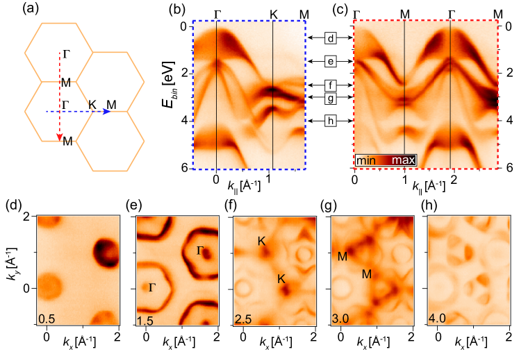
An overview of the electronic band structure of pristine GaSe is presented in Fig. 2. The data are acquired at a photon energy of 94 eV, which probes around the point, as described by the BZ sketches in Fig. 2(a). Figures 2(b)-(c) show cuts along the and high symmetry directions as signified by the dashed lines in Fig. 2(a). The evolution of the dispersion with binding energy is presented via the constant binding energy cuts in Fig. 2(d)-(h), which reveal the trigonal symmetry of the dispersion as well as strong intensity variations between the bands in the BZs. The valence band maximum (VBM) is situated at and is characterized by a parabolic-shaped lobe. The location of the VBM at is consistent with theoretical predictions that GaSe is a direct-gap semiconductor with the conduction band minimum (CBM) also located at Olguín et al. (2013). Additional sub bands dispersing towards and appear above binding energies of 1.5 eV. The material remains rather featureless away from before the onset of this higher binding energy range, implying most of the optical properties of GaSe will derive from the central parabolic lobe. The ARPES data discussed here are fully consistent with the electronic structure data presented in Ref. 34.
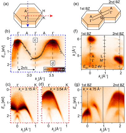
We investigate the -dispersion in the three dimensional BZ of GaSe shown in Fig. 3(a). By measuring the photon energy dependence of the dispersion at normal emission we are able to trace the band structure along the direction, as seen in Fig. 3(b). A strong -dispersion is visible in the center of the parabolic lobe, which is further highlighted via the fits (open circles) and guide line in Fig. 3(b), whereas the bands at binding energies higher than 1.5 eV have a much more flat -dispersion. The fitted dispersion reveals an apparent BZ doubling effect; however, this occurs due to a suppression of the photoemission intensity in adjacent BZsPlucinski et al. (2003), similar to observations in photoemission experiments on graphiteShirley et al. (1995); Mucha-Kruczyński et al. (2008). The band structure along the line is shown for two neighboring BZs in the direction in Fig. 3(c-d). The main intensity moves from the bottom corners of the parabolic lobe in Fig. 3(c) to the VBM in Fig. 3(d). Similar intensity variations are observed in neighboring in-plane BZs, as sketched in Fig. 3(e). The (, )-contour at a binding energy of 0.2 eV shown in Fig. 3(f) shows a cut around the VBM for the plane (see Fig. 3(e)). The intensity maxima are seen to shift between the 1st and 2nd BZs and the absolute intensity levels also vary strongly within the same BZ. A cut along the line at = 4.75 Å-1 in Fig. 3(g) shows the upper VB parabolic lobe in two neighboring zones. In the first BZ, the intensity is concentrated in the bottom corner while in the 2nd BZ the intensity is concentrated around the VBM.
This behavior can be reconciled with the orbital character of the bands, previously studied with detailed calculationsRybkovskiy et al. (2014). Since the states near the VBM are mainly of Se character, the interlayer interactions will cause intensity modulations reflecting the coupling of the GaSe tetralayers, leading to a dispersion resembling a single tetralayer for the value used for the slice shown in Fig. 3(c), while the value for Fig. 3(d) shows a dispersion with a more bulk-like characterRybkovskiy et al. (2014). The subbands just below the VBM exhibit less dramatic behavior due to the character of these states which are less sensitive to the adjacent GaSe tetralayersCamara et al. (2002); Nagel et al. (1979).
III.3 Potassium Deposition of GaSe
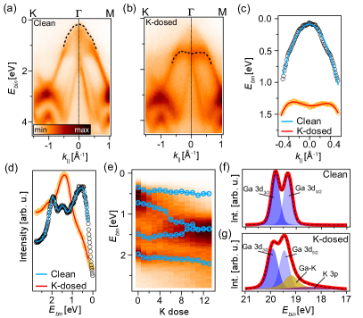
The effect of K dosing of bulk GaSe is explored in Fig. 4. Alkali metal deposition offers a possibility to chemically donate electrons near the surface of GaSe and thereby dope the material. The ARPES measurements along the direction in Fig. 4(a-b) before and after complete K dosing show that a significant band structure change occurs, rather than strong electron doping. A maximum energy shift of 0.1 eV of the VB towards higher binding energies is observed, which may originate from surface band bending due to the added charge or a slight doping of the material. After further dosing, we observe that the spectral weight shifts from the top (see Fig. 4(a)) to the bottom (see Fig. 4(b)) of the VB lobe. In Fig. 4(c), the VBM dispersion (open circles), extracted via fits to energy distribution curves (EDCs), has been fitted with 2nd and 4th order polynomial functions in the clean and K doped cases, respectively. In the pristine GaSe, a global VBM is observed at and at a binding energy of (0.09 0.03) eV. The effective mass around the top of the parabola is = (1.1 0.2), where is the free electron mass. In K dosed GaSe, the VBM splits off into two maxima located at 0.3 Å-1 with a binding energy of (1.30 0.04) eV and an effective mass of = (1.7 0.2).
The EDCs extracted at normal emission in Fig. 4(d) trace the peak positions at each K dosing step. Voigt line shapes have been fitted to each of the peaks, which have been plotted together with the photoemission intensity at normal emission at each K dose in Fig. 4(e), revealing a gradual shift of the ARPES intensity from the pristine bulk dispersion seen in Fig. 4(a) to the modified dispersion shown in Fig. 4(b). The modified dispersion strongly resembles the “bow-shape” or“inverted sombrero” dispersion of single-layer GaSe, where the inversion of the VB is characterized by the energy difference between the VBM and the local energy minimum at Rybkovskiy et al. (2014); Jung et al. (2015); Rybkovskiy et al. (2011); Ben Aziza et al. (2018); Chen et al. (2018). Here, we find that the band inversion is (48 12) meV, which compares well with a value of 80 meV obtained from recent DFT calculationsBen Aziza et al. (2018). The value is substantially smaller than 120 meV found for single-layer GaSe grown on graphene on silicon carbideChen et al. (2018) and than the value of (150 +/- 10) meV that we determine for the similar dispersion at Å-1 in Fig. 3(c). We expect that interlayer interactions between the Se orbitals play a significant role for these dispersion changes around the VBMRybkovskiy et al. (2014) and that the gradual change observed in Fig. 4(e) signals a modification of the topmost GaSe layer, leading to a weaker coupling to the underlying bulk. This may be facilitated by K intercalation in the van der Waals gap between the layers, as observed in metallicRossnagel et al. (2005), and semiconductingEknapakul et al. (2014) transition metal dichalcogenides, or by a chemical interaction on the surface of the crystal, which significantly changes the coupling between individual layers as seen in graphene multilayersOhta et al. (2006, 2007). In these situations one may also expect a change of the interlayer separation of tetralayers as well as a shift of inner potential, which also contribute to the spectral changes we observe. The possibility of chemical changes near the surface is further supported by the observation of an additional core level component in the binding energy range between the Ga 3d and K 3p core levels for the K-dosed sample, which is demonstrated by the comparison between the clean GaSe core level spectrum in Fig. 4(f) and the spectrum for the fully K-dosed sample in Fig. 4(g).
III.4 ARPES and PL Measurements of GaSxSe1-x
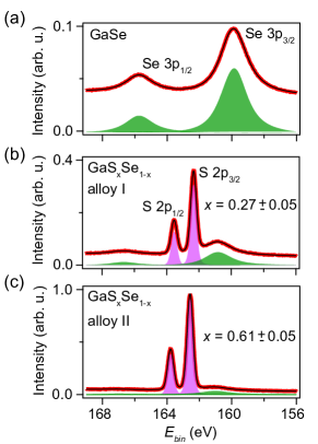
GaSxSe1-x alloys offer a promising route to tune the optical gap and luminescent properties of III-VI semiconductors. However, it is unknown how robust the electronic structure remains between different alloys. Here we compare pristine GaSe with two different GaSxSe1-x alloys (alloys I and II). The stoichiometry is checked via core level measurements of the Se 3p and S 2p binding energy regions, shown in Fig. 5. By comparing the spectral weight of the Se 3p core levels, we are able to estimate that the composition of alloy I is x = 0.27 0.05 and the composition of alloy II is x = 0.61 0.05. These values are consistent when we perform the same analysis on the Se 3d core levels (not shown). The core level data is in agreement with the stoichiometry of precursor added to the growth ampoule.
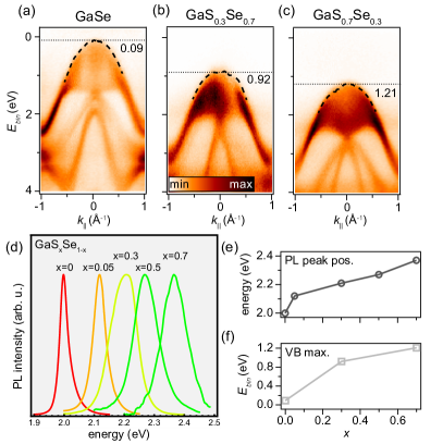
Figure 6(a)-(c) present ARPES measurements of the VBs for the three systems. The overall band dispersion is found to be very similar with a constant effective mass of = (1.1 0.2). The binding energy position of the VBM changes significantly between the three systems, indicating a change of the electronic band gap. It is also possible that Fermi level pinning plays a strong role for the band positions, as the defect concentration is likely different in the alloys. PL measurements, shown in Fig. 6(d), reveal a change of the optical gap. The PL peak positions plotted in Fig. 6(e) show that the optical gap increases as more S is added in the alloy. The same trend is seen for the VBM binding energy position in Fig. 6(f), which fits with a simultaneous increase of the quasiparticle band gap. The trend determined here is fully consistent with optical absorption measurements of GaSxSe1-xJung et al. (2015). Note that ARPES measurements of pure GaS were attempted but the sample was found to charge too severely, which is likely due to the larger band gap of the material compared to the other GaSxSe1-x compounds investigated here.
The and stacking phases observed in HRSTEM are not expected to give rise to striking differences in the electronic structureCamara et al. (2002); Nagel et al. (1979); Rybkovskiy et al. (2011). However, detailed inspection of the measurements in Fig.. 6(a)-(c) does show some variation in the intensity and structure of the dispersive bands in the higher binding energy region above the central VB lobe. While different stacking phases may affect the photoemission intensity, the change in chemical environment caused by the mixed chalcogen content directly influences the in-plane px(y) orbitals that the higher binding energy bands are composed of, thereby leading to the possibility of a modified dispersion.
IV Conclusion
We have measured the bulk electronic structure of GaSe using ARPES and thereby identified the bulk band dispersion, the structure of the VBM, and the complex photoemission intensity variations associated with the tetralayer unit cell. Potassium deposition of GaSe leads to a dramatic change of the VBM dispersion from a parabolic shape characteristic for the bulk to an inverted bow-like shape that is usually associated with single-layer samples. Our data are consistent with an increased band gap and a transition from a direct to an indirect band gap semiconductor, which is caused by a strong modification of the top-most GaSe tetralayer due to the interaction with the deposited K atoms. We have investigated the effect of sulfur alloying on the crystalline and electronic structure and used HRSTEM to observe a transition from the phase to the phase for sulfur content above 30 percent. We have also shown that alloying causes a rigid shift of the VBM binding energy position without a significant change in the actual band dispersion around the VBM. This rigid shift is consistent with an increase in the optical band gap measured by PL.
Acknowledgements.
This work was supported primarily by the U.S. Department of Energy, Office of Science, Office of Basic Energy Sciences, Materials Sciences and Engineering Division, under Contract No. DE-AC02-05CH11231, within the van der Waals Heterostructures Program (KCWF16), which provided for HRSTEM and ARPES support. This work was also supported in part by the National Science Foundation under Grant No. DMR-1807233, which provided for PL measurements and preliminary exploration of sample growth parameters. S.U. acknowledges financial support from VILLUM FONDEN under the Young Investigator Program (Grant No. 15375). R.J.K. was supported by a fellowship within the Postdoc-Program of the German Academic Exchange Service (DAAD). The Advanced Light Source is supported by the Director, Office of Science, Office of Basic Energy Sciences, of the U.S. Department of Energy under Contract No. DE-AC02-05CH11231. Work at the Molecular Foundry was supported by the Office of Science, Office of Basic Energy Sciences, of the US Department of Energy under Contract No. DE-AC02-05CH11231. B.S. acknowledges support from the NSF LSAMP BD graduate fellowship.References
- Wasala et al. (2017) M. Wasala, H. I. Sirikumara, Y. Raj Sapkota, S. Hofer, D. Mazumdar, T. Jayasekera, and S. Talapatra, J. Mater. Chem. C 5, 11214 (2017).
- Novoselov et al. (2004) K. S. Novoselov, A. K. Geim, S. V. Morozov, D. Jiang, Y. Zhang, S. V. Dubonos, I. V. Grigorieva, and A. A. Firsov, Science 306, 666 (2004).
- Feng et al. (2011) J. Feng, X. Sun, C. Wu, L. Peng, C. Lin, S. Hu, J. Yang, and Y. Xie, Journal of the American Chemical Society 133, 17832 (2011).
- Mak et al. (2010) K. F. Mak, C. Lee, J. Hone, J. Shan, and T. F. Heinz, Phys. Rev. Lett. 105, 136805 (2010).
- Splendiani et al. (2010) A. Splendiani, L. Sun, Y. Zhang, T. Li, J. Kim, C.-Y. Chim, G. Galli, and F. Wang, Nano Lett. 10, 1271 (2010).
- Watanabe et al. (2004) K. Watanabe, T. Taniguchi, and H. Kanda, Nat. Mater. 3, 404 (2004).
- Guillamón et al. (2008) I. Guillamón, H. Suderow, S. Vieira, L. Cario, P. Diener, and P. Rodière, Phys. Rev. Lett. 101, 166407 (2008).
- Navarro-Moratalla et al. (2016) E. Navarro-Moratalla, J. O. Island, S. Mañas-Valero, E. Pinilla-Cienfuegos, A. Castellanos-Gomez, J. Quereda, G. Rubio-Bollinger, L. Chirolli, J. A. Silva-Guillén, N. Agraït, G. A. Steele, F. Guinea, H. S. J. van der Zant, and E. Coronado, Nat. Commun. 7, 11043 (2016).
- Ugeda et al. (2015) M. M. Ugeda, A. J. Bradley, Y. Zhang, S. Onishi, Y. Chen, W. Ruan, C. Ojeda-Aristizabal, H. Ryu, M. T. Edmonds, H.-Z. Tsai, A. Riss, S.-K. Mo, D. Lee, A. Zettl, Z. Hussain, Z.-X. Shen, and M. F. Crommie, Nat. Phys. 12, 92 (2015).
- Liu et al. (2018) G. Liu, S. Rumyantsev, M. A. Bloodgood, T. T. Salguero, and A. A. Balandin, Nano Lett. (2018).
- Xi et al. (2015) X. Xi, L. Zhao, Z. Wang, H. Berger, L. Forró, J. Shan, and K. F. Mak, Nat. Nanotechnol. 10, 765 (2015).
- Choi et al. (2017) W. Choi, N. Choudhary, G. H. Han, J. Park, D. Akinwande, and Y. H. Lee, Materials Today 20, 116 (2017).
- Rybkovskiy et al. (2014) D. V. Rybkovskiy, A. V. Osadchy, and E. D. Obraztsova, Phys. Rev. B Condens. Matter 90, 235302 (2014).
- Cai et al. (2016) H. Cai, E. Soignard, C. Ataca, B. Chen, C. Ko, T. Aoki, A. Pant, X. Meng, S. Yang, J. Grossman, F. D. Ogletree, and S. Tongay, Advanced Materials 28 (2016).
- Robertson (2001) J. Robertson, J. Phys. C: Solid State Phys. 12 (2001).
- Lei et al. (2013) S. Lei, L. Ge, Z. Liu, S. Najmaei, G. Shi, G. You, J. Lou, R. Vajtai, and P. M. Ajayan, Nano Letters 13, 2777 (2013).
- Ben Aziza et al. (2017) Z. Ben Aziza, D. Pierucci, H. Henck, M. G. Silly, C. David, M. Yoon, F. Sirotti, K. Xiao, M. Eddrief, J.-C. Girard, and A. Ouerghi, Phys. Rev. B 96, 035407 (2017).
- Hu et al. (2012) P. Hu, Z. Wen, L. Wang, P. Tan, and K. Xiao, ACS Nano 6, 5988 (2012).
- Zhou et al. (2014) Y. Zhou, Y. Nie, Y. Liu, K. Yan, J. Hong, C. Jin, Y. Zhou, J. Yin, Z. Liu, and H. Peng, ACS Nano 8, 1485 (2014).
- Late et al. (2012) D. J. Late, B. Liu, J. Luo, A. Yan, H. S. S. R. Matte, M. Grayson, C. N. R. Rao, and V. P. Dravid, Advanced Materials 24, 3549 (2012).
- Serizawa et al. (1980) H. Serizawa, Y. Sasaki, and Y. Nishina, Journal of the Physical Society of Japan 48, 490 (1980).
- Jung et al. (2015) C. S. Jung, F. Shojaei, K. Park, J. Y. Oh, H. S. Im, D. M. Jang, J. Park, and H. S. Kang, ACS Nano (2015), 10.1021/acsnano.5b04876.
- Chen et al. (2015) H. Chen, Y. Li, L. Huang, and J. Li, Rsc Adv 5, 50883 (2015).
- Del Pozo-Zamudio et al. (2015) O. Del Pozo-Zamudio, S. Schwarz, M. Sich, I. A. Akimov, M. Bayer, R. C. Schofield, E. A. Chekhovich, B. J. Robinson, N. D. Kay, O. V. Kolosov, A. I. Dmitriev, G. V. Lashkarev, D. N. Borisenko, N. N. Kolesnikov, and A. I. Tartakovskii, 2D Materials 2 (2015).
- Kim et al. (2016) W. Kim, C. Li, F. A. Chaves, D. Jiménez, R. D. Rodriguez, J. Susoma, M. A. Fenner, H. Lipsanen, and J. Riikonen, Advanced Materials 28, 1845 (2016).
- Ben Aziza et al. (2016) Z. Ben Aziza, H. Henck, D. Pierucci, M. G. Silly, E. Lhuillier, G. Patriarche, F. Sirotti, M. Eddrief, and A. Ouerghi, ACS Nano (2016).
- Li et al. (2015) X. Li, L. Basile, B. Huang, C. Ma, J. Lee, I. Vlassiouk, A. Puretzky, M. Lin, M. Yoon, M. Chi, J. Idrobo, C. Rouleau, B. Sumpter, D. Geohegan, and K. Xiao, Acs Nano 9, 8078 (2015).
- Ni et al. (2013) Y. Ni, H. Wu, C. Huang, M. Mao, Z. Wang, and X. Cheng, Journal of Crystal Growth 381, 10 (2013).
- Hüfner (2003) S. Hüfner, Photoelectron Spectroscopy, 3rd ed. (Springer, Berlin, 2003).
- Whitehouse and Balchin (1978) C. Whitehouse and A. Balchin, Journal of Materials Science 13, 2394 (1978).
- Terhell et al. (1982) J. Terhell, V. Brabers, and G. van Egmond, Journal of Solid State Chemistry 41, 97 (1982).
- Arancia et al. (1976) G. Arancia, M. Grandolfo, C. Manfredotti, and A. Rizzo, physica status solidi (a) 33, 563 (1976).
- Olguín et al. (2013) D. Olguín, A. Rubio-Ponce, and A. Cantarero, Eur. Phys. J. B 86, 350 (2013).
- Plucinski et al. (2003) L. Plucinski, R. Johnson, B. Kowalski, K. Kopalko, B. Orlowski, Z. Kovalyuk, and G. Lashkarev, Physical Review B 68, 125304 (2003).
- Shirley et al. (1995) E. L. Shirley, L. J. Terminello, A. Santoni, and F. J. Himpsel, Physical Review B 51, 13614 (1995).
- Mucha-Kruczyński et al. (2008) M. Mucha-Kruczyński, O. Tsyplyatyev, A. Grishin, E. McCann, V. I. Fal’ko, A. Bostwick, and E. Rotenberg, Physical Review B 77, 195403 (2008).
- Camara et al. (2002) M. Camara, A. Mauger, and I. Devos, Physical Review B 65, 125206 (2002).
- Nagel et al. (1979) S. Nagel, A. Baldereschi, and K. Maschke, Journal of Physics C: Solid State Physics 12, 1625 (1979).
- Rybkovskiy et al. (2011) D. Rybkovskiy, N. Arutyunyan, A. Orekhov, I. Gromchenko, I. Vorobiev, A. Osadchy, E. Y. Salaev, T. Baykara, K. Allakhverdiev, and E. Obraztsova, Physical Review B 84, 085314 (2011).
- Ben Aziza et al. (2018) Z. Ben Aziza, V. Zólyomi, H. Henck, D. Pierucci, M. G. Silly, J. Avila, S. J. Magorrian, J. Chaste, C. Chen, M. Yoon, K. Xiao, F. Sirotti, M. C. Asensio, E. Lhuillier, M. Eddrief, V. I. Fal’ko, and A. Ouerghi, Physical Review B 98, 115405 (2018).
- Chen et al. (2018) M.-W. Chen, H. Kim, D. Ovchinnikov, A. Kuc, T. Heine, O. Renault, and A. Kis, npj 2D Materials and Applications , 1 (2018).
- Rossnagel et al. (2005) K. Rossnagel, E. Rotenberg, H. Koh, N. V. Smith, and L. Kipp, Physical Review Letters 95, 126403 (2005).
- Eknapakul et al. (2014) T. Eknapakul, P. D. C. King, M. Asakawa, P. Buaphet, R.-H. He, S.-K. Mo, H. Takagi, K. M. Shen, F. Baumberger, T. Sasagawa, S. Jungthawan, and W. Meevasana, Nano Letters 14, 1312 (2014).
- Ohta et al. (2006) T. Ohta, A. Bostwick, T. Seyller, K. Horn, and E. Rotenberg, Science 313, 951 (2006).
- Ohta et al. (2007) T. Ohta, A. Bostwick, J. L. McChesney, T. Seyller, K. Horn, and E. Rotenberg, Physical Review Letters 98, 206802 (2007).