Strain-engineering of Berry curvature dipole and
valley magnetization in monolayer MoS2
Abstract
The Berry curvature dipole is a physical quantity that is expected to allow various quantum geometrical phenomena in a range of solid-state systems. Monolayer transition metal dichalcogenides provide an exceptional platform to modulate and investigate the Berry curvature dipole through strain. Here we theoretically demonstrate and experimentally verify for monolayer MoS2 the generation of valley orbital magnetization as a response to an in-plane electric field due to the Berry curvature dipole. The measured valley orbital magnetization shows excellent agreement with the calculated Berry curvature dipole which can be controlled by the magnitude and direction of strain. Our results show that the Berry curvature dipole acts as an effective magnetic field in current-carrying systems, providing a novel route to generate magnetization.
Berry curvature is central to various topological phenomena observed in solid-state crystals Xiao2010 , ultracold atoms Tarruell2012 ; Aidelsburger2013 and photonic architectures Lu2014 . In view of charge transport, its effect has been assumed to be limited to magnetic systems with broken time reversal symmetry as hallmarked by the anomalous Hall effect Nagaosa2010 . Recent theories, however, demonstrated that in nonlinear regime, Hall effect can occur even in time-reversal symmetric systems if they are noncentrosymmetric and possess reduced symmetry (e.g., only one mirror plane) Sodemann2015 ; Low2015 . The nonlinear Hall effect has been attributed to the dipole moment formation of the Berry curvature in momentum space. Such Berry curvature dipole widens the scope of Berry curvature effects. It was recently proposed that in transition metal dichalcogenides (TMDs), the Berry curvature dipole may be generated when spatial symmetries of TMDs are lowered by strain Sodemann2015 ; You2018 . This motivates monolayer TMDs as promising materials venue to examine the Berry curvature dipole. As exemplified by ultracold gases, where the in-depth examination of the Berry curvature effects becomes possible through the Berry curvature variation by the optical lattice modulation Tarruell2012 ; Aidelsburger2013 , the mechanical tunability of the Berry curvatures in TMDs provides an ideal avenue to explore the Berry curvature dipole.
TMDs are noncentrosymmetric two dimensional materials and have two nonequivalent and valleys holding the opposite signs of the Berry curvature Xiao2012 (Fig. 1(a)). Such valley-dependent Berry curvature gives rise to intriguing phenomena Xu2014 ; Mak2018 such as the valley optical selection rule Cao2012 ; Mak2012 ; Zeng2012 , the valley Zeeman effect Li2014 ; MacNeill2015 ; Srivastava2015 ; Aivazian2015 and the valley Hall effect Mak2014 ; Lee2016 ; Lee2017 . Further manipulation of electrically induced valley magnetization has been demonstrated by lowering the crystal symmetries of TMDs by strain Lee2017 , but the dependence on strain yet remains unclear. Given the inherent flexibility of monolayer TMDs, comprehensive studies on strain dependence may allow simultaneous investigation of the valley magnetization and Berry curvature dipole. In this work, we employ stretchable van der Waals heterostructures and demonstrate that the strain-induced Berry curvature dipole in monolayer molybdenum disulfide (MoS2) generates electrically induced valley orbital magnetization. The magnitude and direction of the valley orbital magnetization are directly probed by Kerr rotation microscopy as a function of strain, which shows an excellent agreement with calculated Berry curvature dipole. The observed valley magnetization increases with the increasing magnitude of strain and reversibly turns on and off and flips the sign depending on the direction of strain. Our approach demonstrates strain engineering as a distinct pathway to control the valley degree of freedom in monolayer TMDs and provides a precision tool to map out the Berry curvature dipole in solid-state crystals.
The van der Waals heterostructures in our work consist of monolayer MoS2, few-layer (FL) graphene and hexagonal boron nitride (h-BN) as shown in Fig. 1(b). The exfoliated monolayer MoS2 crystal is first transferred onto a flexible substrate with pre-patterned metal pads. Then two FL graphene exfoliated onto SiO2/Si substrate are picked up by h-BN using poly-propylene carbonate (PPC). The h-BN and two graphene stack is transferred onto MoS2 to form source and drain electrodes. The h-BN capping layer, with a thickness around 20 nm unless otherwise noted, minimized the exposure of MoS2 to air and enhanced the adhesion between MoS2 and substrate. The final device image is shown in Fig. 1(c). We note that all our measurements in this work are performed at room temperature.
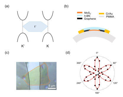
To apply strain in desired directions, the crystal orientation of the MoS2 is identified by the polarization-resolved second harmonic generation (SHG) Li2013 ; Malard2013 . In this measurement, the SH intensity component parallel to the polarization of the pump laser is detected. Fig. 1(d) shows the polar plot of the SH intensity measured as a function of the laser polarization angle, which shows the maximum intensity when the polarization aligns to the armchair direction of the crystal (Methods in Supplementary Materials).
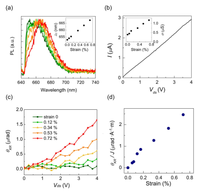
With information on the crystal orientation, we applied strain in the armchair direction of the crystal by bending the substrate. The magnitude of strain is obtained from the bent geometry of the substrate and further confirmed by photoluminescence (PL) measurement of MoS2 (Fig. 2(a)). The PL red-shifts of 20 nm per strain percent is repeatedly observed from several different devices, showing the accurate determination of strain level in our experiment (Supplementary Materials Fig. S1). The observed shift ratio reflects the strain-induced modification of the bandgap which is independent of the strain direction He2013 . The curve is monitored on the same device as shown in Fig. 2(b). The measured conductance is found to increase with strain because of the increasing contact area between graphene and MoS2 caused by bending.
While applying strain on the device, the magnetization of MoS2 is simultaneously measured at the channel center as functions of strain and an in-plane bias. The magnetization is directly probed by using the Kerr rotation (KR) spectroscopy. For KR measurement, a linearly polarized laser with a wavelength tuned to the transition resonance of MoS2 is focused onto the sample and polarization rotation () of the probe laser upon reflection is measured by balanced detectors (Methods in Supplementary Materials). To increase the signal-to-noise ratio, we measured that is frequency-locked to the alternating bias applied to the source electrode. When there is no strain applied to MoS2, negligible is measured at a finite bias. However, by applying strain, nonzero is detected which increases with strain and an in-plane bias (Fig. 2(c)). To examine the dependence of on strain under the same current level, normalized by the channel current density () is plotted as a function of strain in Fig. 2(d). The measured / shows linear dependence on the magnitude of strain. Similar strain and bias dependence of / is measured from several different devices as exemplified in Supplementary Materials Fig. S2.
We then investigated the strain direction dependence of the magnetization as shown in Fig. 3. The armchair direction of monolayer MoS2 in this device is aligned parallel to graphene electrodes so that the channel current flows in the zigzag direction () of the crystal, and tensile strain is applied in one of zigzag () or armchair () direction. For this measurement, on the entire channel is imaged as a function of position by scanning the sample position. Fig. 3(a) shows null KR map of the device when there is no strain under a finite bias voltage ( = 3.5 V). Under the same bias, by applying strain along as shown in Fig. 3(b), a finite with positive sign is measured on the entire channel. From the 2D scan map of that was detected primarily on MoS2 channel area, we confirm that the measured signal originates from the magnetization of MoS2. Also, the measured values of Kerr rotation as well as Kerr ellipticity showed negligible dependence on the probe polarization angle, ruling out the possibility that the strain- or current-induced birefringence is detected (Supplementary Materials Fig. S3). Then we released the strain and applied the same amount of strain again along (PL data in Supplementary Materials Fig. S4). Surprisingly, the sign of changes all over the channel under the armchair strain (Fig. 3(c)). The direction and magnitude of the channel current were maintained to be the same under two different strain directions. Below we show that the observed magnetization in monolayer MoS2 that is switchable with strain at room temperature is possible due to the mechanical control of the Berry curvature dipole.
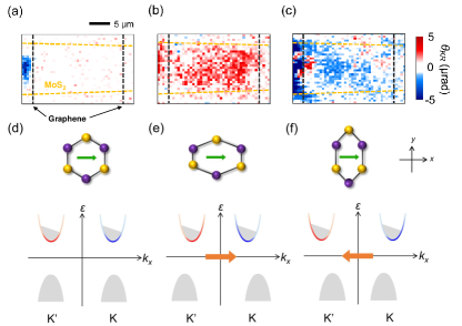
To verify the origin of the observed magnetization, we performed a tight binding model calculation and obtained energy band and Berry curvature distribution of monolayer MoS2 at different strains Neto2009 ; Vozmediano2010 ; Peng2013 ; Gomez2013 ; Zhang2013 ; Rostami2015 . Details can be found in Supplementary Materials Sec. 3.1. In short, the application of strain modifies the Berry curvature () distribution about and points (red and blue colors of conduction band). Unlike pristine monolayer MoS2, the application of strain shifts the band edge in the opposite directions depending on the strain orientation as shown in Fig. 3(e) and (f). Note that becomes asymmetric with respect to the bottom of the conduction band, implying the emergence of the Berry curvature dipole () (marked by orange arrows), where [6]. Here, is the crystal momentum, is the electron occupation function and . For pristine monolayer MoS2 with 3-fold rotational symmetry, (Fig. 3(d)). Strained monolayer MoS2, on the other hand, possesses asymmetric leading to the nonvanishing which is perpendicular to the mirror plane and thus aligned along the crystal’s mirror line, i.e., . More interestingly, the direction of is opposite for two different strain directions; along the zigzag (Fig. 3(e)) and armchair (Fig. 3(f)).
We now demonstrate that strain-induced Berry curvature dipole becomes the source of magnetization when there is an in-plane electric field. Consider the orbital magnetization () defined as Xiao2005 ; Yoda2015
| (1) |
where is the thickness of the monolayer MoS2, is the orbital magnetic moment, is the chemical potential and is the energy dispersion of the conduction band. Here we assume that MoS2 is weakly -doped with partially occupied conduction band. Weak spin splitting of the conduction band is ignored. When an external electric field is applied, is given by , where is the equilibrium Fermi-Dirac distribution function and is the electron mean free time. Since vanishes in equilibrium with , in the presence of the driving field becomes . Here it is used that is proportional to . Considering the relation near the bottom of the MoS2 conduction band, where is the energy gap at and points, and by using the definition of the Berry curvature dipole, we obtain the relation
| (2) |
In this simplified equation, the valley magnetization is generated as a linear response to , which is regulated by the Berry curvature dipole . Note that the Berry curvature dipole was originally introduced in the quantum nonlinear Hall effect Sodemann2015 ; Low2015 which relates the Hall current density as a quadratic response of : . Interestingly, both and support that can be interpreted as an effective magnetic field. Out of the two ’s responsible for , one induces magnetization and effectively breaks the time-reversal symmetry and the other induces the anomalous Hall effect in the presence of the magnetization.
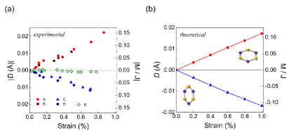
Eq. (2) explains many important features observed in our experiment. First, reversing the direction of or flips the direction of the out-of-plane magnetization . In Fig. 3(e) and (f), we illustrate the band structures for two different directions of under the same . The resulting flips the sign upon reversing , which is clearly demonstrated in Fig. 3(b) and (c). We have also checked the case when is reversed while maintaining , which also changes the direction of (Supplementary Materials Fig. S5). Second, nonzero is generated only when and have a collinear component. Since is always generated along the zigzag direction of the crystal, a finite requires to be applied along the same zigzag direction. On the other hand, if is applied perpendicular to , i.e., along an armchair, no magnetization will arise even under a finite strain and an in-plane electric field. Such case is investigated with a device with the channel current flowing along the armchair direction of a crystal, from which no magnetization is measured with increasing strain (green diamonds in Fig. 4(a)). Detailed device structure and measurement results can be found in Supplementary Materials Fig. S6.
The measured valley magnetization is also in a quantitative agreement with theoretical calculations. Fig. 4(a) shows the magnetization normalized by current, , which is converted from the measured value of / in several different monolayer MoS2 from the same bulk. In the conversion, we considered that is the result of the absorbance difference between right- and left-handed light at the probe wavelength. Such circular dichroism () can also be directly related to the Berry curvature dipole through , where is the thermal transition linewidth broadening Xiao2012 ; Lee2017 ; Yao2008 (Supplementary Materials Sec. 3.2). Note that the expression for is similar to that of the valley magnetization because both quantities have the same origin, i.e., electron occupation enclosing asymmetric Berry curvature distribution at and valleys. The experimental is then obtained from in Eq. (2).
Fig. 4(b) shows the calculated Berry curvature dipole using the tight-binding model when the Fermi energy is 30 meV above the conduction band minimum, roughly matching the doping density of our MoS2 crystal, . The calculated and is linearly proportional to the magnitude of strain and has opposite signs for two different strain directions. The magnitude of theoretical Berry curvature dipole and normalized magnetization are in remarkable agreement with experimental results, suggesting that our method will also be applicable to probe the Berry curvature dipole in other materials.
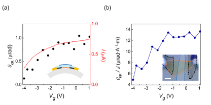
Finally, we investigated the doping density dependence of the valley magnetization by fabricating a monolayer MoS2 transistor. In this experiment, a FL graphene is additionally stacked on top of the MoS2/graphene/h-BN heterostructure to apply a gate voltage as shown in Fig. 5. A relatively thick h-BN ( nm) is used as an insulating layer to avoid coupling between source and gate electrodes. Strain and in-plane electric fields in this device are applied in the same zigzag direction to produce substantial valley magnetization. Detailed strain dependent measurements are shown in the Supplementary Materials Fig. S7. Here we focus on the gate dependence of at a fixed strain of 0.28 % when V (Fig. 5(a)). From the measurement, both and channel current increase with increasing gate voltage. In Fig. 5(b), increases with gate voltage and eventually saturates. Our observation is well explained by the calculated valley magnetization as a function of Fermi energy (Supplementary Materials Fig. S11). Since the Berry curvature dipole represents the degree of asymmetry of Berry curvature distribution and because of the parabolic shape of band structure, the increasing rate of Berry curvature dipole with doping is the largest at the band edge.
In conclusion, our work shows that applying strain to monolayer TMD induces the Berry curvature dipole depending on the direction and magnitude of strain. The Berry curvature dipole enables the mechanical tuning of valley magnetization excited by an in-plane electric field. By employing strain as a new functionality, monolayer TMDs could potentially be useful for novel valley flexomagnetic and memory devices. Through advance in strain engineering of monolayer materials in combination with conventional technologies, e.g., piezoelectric modulation Wu2014 ; Akinwande2014 , new opportunities for strain-mediated valley-charge conversion may also emerge. Our work further envisages the Berry curvature dipole as a tunable source of magnetization in other systems with quantum geometric properties Xu2018 ; Ma2018 ; Kang2019 .
The authors thank fruitful discussions with Kin Fai Mak and Jie Shan. The authors also acknowledge support from the National Research Foundation (NRF) of Korea (Grants No. 2017R1C1B2002631, No. 2018R1A5A6075964 and No. 2018R1A5A6086814). J. L. was supported by TJ Park Science Fellowship of POSCO TJ Park Foundation. Theoretical analysis of K.-H. K. and H.-W. L. was supported by the SSTF (BA-1501-07).
References
- (1) D. Xiao, M.-C. Chang, and Q. Niu, Rev. Mod. Phys. 82, 1959 (2010).
- (2) L. Tarruell, D. Greif, T. Uehlinger, G. Jotzu, and T. Esslinger, Nature 483, 302 (2012).
- (3) M. Aidelsburger, M. Atala, M. Lohse, J. T. Barreiro, B. Paredes, and I. Bloch, Phys. Rev. Lett. 111, 185301 (2013).
- (4) L. Lu, J. D. Joannopoulos, and M. Soljacic, Nat. Photonics 8, 821 (2014).
- (5) N. Nagaosa, J. Sinova, S. Onoda, A. H. MacDonald, and N. P. Ong, Rev. Mod. Phys. 82, 1539 (2010).
- (6) I. Sodemann and L. Fu, Phys. Rev. Lett. 115, 216806 (2015).
- (7) T. Low, Y. Jiang, and F. Guinea, Phys. Rev. B 92, 235447 (2015).
- (8) J. S. You, S. Fang, S. Y. Xu, E. Kaxiras, and T. Low, Phys. Rev. B 98, 121109(R) (2018).
- (9) D. Xiao, G.-B. Liu, W. Feng, X. Xu, and W. Yao, Phys. Rev. Lett. 108, 196802 (2012).
- (10) X. Xu, W. Yao, D. Xiao, and T. F. Heinz, Nat. Phys. 10, 343 (2014).
- (11) K. F. Mak, D. Xiao, and J. Shan, Nat. Photonics 12, 451 (2018).
- (12) T. Cao, G. Wang, W. Han, H. Ye, C. Zhu, J. Shi, Q. Niu, P. Tan, E. Wang, B. Liu, and J. Feng, Nat. Commun. 3, 887 (2012).
- (13) K. F. Mak, K. He, J. Shan, and T. F. Heinz, Nat. Nanotech. 7, 494 (2012).
- (14) H. Zeng, J. Dai, W. Yao, D. Xiao, and X. Cui, Nat. Nanotech. 7, 490 (2012).
- (15) Y. Li, J. Ludwig, T. Low, A. Chernikov, X. Cui, G. Arefe, Y. D. Kim, A. M. vanderZande, A. Rigosi, H. M. Hill, S. H. Kim, J. Hone, Z. Li, D. Smirnov, and T. F. Heinz, Phys. Rev. Lett. 113, 266804 (2014).
- (16) D. MacNeill, C. Heikes, K. F. Mak, Z. Anderson, A. Kormanyos, V. Zolyomi, J. Park, and D. C. Ralph, Phys. Rev. Lett. 114, 037401 (2015).
- (17) A. Srivastava, M. Sidler, A. V Allain, D. S. Lembke, A. Kis, and A. Imamoğlu, Nat. Phys. 11, 141 (2015).
- (18) G. Aivazian, Z. Gong, A. M. Jones, R. L. Chu, J. Yan, D. G. Mandrus, C. Zhang, D. Cobden, W. Yao, and X. Xu, Nat. Phys. 11, 148 (2015).
- (19) K. F. Mak, K. L. McGill, J. Park, and P. L. McEuen, Science 344, 1489 (2014).
- (20) J. Lee, K. F. Mak, and J. Shan, Nat. Nanotechnol. 11, 421 (2016).
- (21) J. Lee, Z. Wang, H. Xie, K. F. Mak, and J. Shan, Nat. Mater. 16, 887 (2017).
- (22) Y. Li, Y. Rao, K. F. Mak, Y. You, S. Wang, C. R. Dean, and T. F. Heinz, Nano Lett. 13, 3329 (2013).
- (23) L. M. Malard, T. V. Alencar, A. P. M. Barboza, K. F. Mak, and A. M. de Paula, Phys. Rev. B 87, 201401(R) (2013).
- (24) K. He, C. Poole, K. F. Mak, and J. Shan, Nano Lett. 13, 2931 (2013).
- (25) A. H. Castro Neto, F. Guinea, N. M. R. Peres, K. S. Novoselov, and A. K. Geim, Rev. Mod. Phys. 81, 109 (2009).
- (26) M. A. H. Vozmediano, M. I. Katsnelson, and F. Guinea, Phys. Rep. 496, 109 (2010).
- (27) Q. Peng and S. De, Phys. Chem. Chem. Phys. 15, 19427 (2013).
- (28) A. Castellanos-Gomez, R. Roldán, E. Cappelluti, M. Buscema, F. Guinea, H. S. J. Van Der Zant, and G. A. Steele, Nano Lett. 13, 5361 (2013).
- (29) Q. Zhang, Y. Cheng, L. Y. Gan, and U. Schwingenschlogl, Phys. Rev. B 88, 245447 (2013).
- (30) H. Rostami, R. Roldan, E. Cappelluti, R. Asgari, and F. Guinea, Phys. Rev. B 92, 195402 (2015).
- (31) D. Xiao, J. Shi, and Q. Niu, Phys. Rev. Lett. 95, 137204 (2005).
- (32) T. Yoda, T. Yokoyama, and S. Murakami, Sci. Rep. 5, 12024 (2015).
- (33) W. Yao, D. Xiao, and Q. Niu, Phys. Rev. B 77, 235406 (2008).
- (34) W. Wu, L. Wang, Y. Li, F. Zhang, L. Lin, S. Niu, D. Chenet, X. Zhang, Y. Hao, T. F. Heinz, J. Hone, and Z. L. Wang, Nature 514, 470 (2014).
- (35) D. Akinwande, N. Petrone, and J. Hone, Nat. Commun. 5, 5678 (2014).
- (36) S. Xu, Q. Ma, H. Shen, V. Fatemi, S. Wu, T. Chang, G. Chang, A. M. M. Valdivia, C. Chan, Q. D. Gibson, J. Zhou, Z. Liu, K. Watanabe, T. Taniguchi, H. Lin, R. J. Cava, L. Fu, N. Gedik, and P. Jarillo-herrero, Nat. Phys. 14, 900 (2018).
- (37) Q. Ma, S. Y. Xu, H. Shen, D. MacNeill, V. Fatemi, T. R. Chang, A. M. Mier Valdivia, S. Wu, Z. Du, C. H. Hsu, S. Fang, Q. D. Gibson, K. Watanabe, T. Taniguchi, R. J. Cava, E. Kaxiras, H. Z. Lu, H. Lin, L. Fu, N. Gedik, and P. Jarillo-Herrero, Nature 565, 337 (2019).
- (38) K. Kang, T. Li, E. Sohn, J. Shan, and K. F. Mak, Nat. Mater. 18, 324 (2019).