A tunnel-field-effect spin-filter from two-dimensional anti-ferromagnetic stanene
Abstract
We propose a device concept, based on monolayer stanene, able to provide highly polarized spin currents (up to a ) with voltage-controlled spin polarization operating at room temperature and with small operating voltage ( V). The concept exploits the presence of spin-polarized edge states in a stanene nanoribbon. The spin polarization of the total current can be modulated by a differential tuning of the transmission properties, and of the occupation of edge states of different spin, via the application of an in-plane electric field. We demonstrate device operation using ab-initio and quantum transport simulations.
Introduction
Spintronics, the application of the electron spin degree of freedom to information technology Wolf01 ; Awschalom07 ; Felser07 , has experimented an impressive progress since the discovery of the giant magneto-resistive effect in late eighties Baibich88 , that was followed and improved, a few years later, by the tunneling magnetoresistance effect Modera1995 . Nowadays, spintronics constitutes a intense research area embracing from physics to computer science Xu2016 ; Zutic2004 , and involving exciting and promising fields as topological insulators Qi2011 and quantum computing Leuenberger2001 .
Indeed, although many issues are still at their infancy including efficient injection, transport, and control of spin currents Avci17 ; Miron11 , enormous progresses have been made, and some notable devices have been proposed and demonstrated, such as, e.g. spin torque memories, Hosomi05 ; Liu12 ; Prenat2015 spin valves in hard drives read heads Tsang1994 , galvanic isolators Hermann1997 , magnetic memories based on tunnel junctions Gallagher2006 , spin transistors Datta1990 and logic devices built from diluted magnetic semiconductors Ohno2000 .
Further progresses are expected to be enabled by the investigation of promising combinations of materials and structures Gao13 ; Ohno16 , including ferromagnetics stacks Jedema01 , half-metals deGroot83 ; Son06 , or spin-gapless semiconductors Wang08 ; Ouardi13 . More recently, the raise of graphene Novoselov04 opened new possibilities in the field Roche15 ; Han14 , unveiling new two-dimensional (2D) materials as potential candidates to be used in spin devices Pesin12 ; Gao16 ; Nie17 ; Ashton17 ; Garcia18 . Specifically for graphene, half-metallicity in zig-zag nanoribbons Son06 ; Kan08 , defect-induced magnetism Yazyev07 ; Bundesman13 and spin transport at room temperature Tombros07 ; Han10 have been predicted and experimentally demonstrated.
In addition to graphene, other column-IV 2D materials Molle17 , like silicene Lay12 , germanene Davila14 and lastly stanene Zhu16 have been recently pointed out to have an stable anti-ferromagnetic ground state when cut in thin zig-zag nanoribbons Wang16 ; Xiong16 . A very promising property for spintronics in graphene, germanene and silicene is the electric-field-controlled half-metallicity, i.e., the possibility to tune the nanoribbon bandgap from semiconducting to zero with a transversal in-plane electric field, that unfortunately is too large (from MV/cm to MV/cm) to be used in realistic applications and with practical dielectrics Son06 ; Wang13 .
In this letter, we explore the appearance of half-metallicity in stanene nanoribbons with first principle calculations, and we propose a device based on interband tunneling able to exploit this effect to generate highly spin-polarized currents with small and realistic electric fields. We have opted for stanene amongst group-IV candidates because it provides a reasonable compromise between the bandgap width (required to avoid high leakages currents) and the transversal electric field necessary to achieve half-metalicity (that must prevent from the dielectric breakdown). In particular, the high sensitivity of interband tunneling to small modulations of the bandgap and its reduced dependence on temperature, together with its robustness against the presence of defects Nanoscale17 , allows us to take advantage of the electric-field-controlled half-metallicity in a tunnel-field-effect transistor (TFET) based on a stanene nanoribbon.
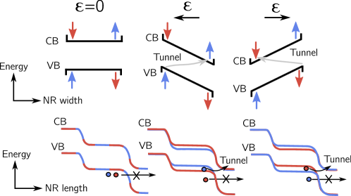
A schematic illustration of device operation is shown in Fig. 1. In a TFET, the source and drain regions are p- and n-doped respectively, pinning the chemical potential at the source/drain close to the valence/conduction band. At equilibrium, i.e, when no external voltages are applied, the chemical potential along the device is constant. When a positive drain-to-source voltage is considered, the chemical potential at the drain is lowered with respect to the source and an energy window for carrier tunneling is open. Then, when no transversal electric field is applied (left) the bandgap at any point along the channel is the same for both kinds of spins. If the source and drain regions are properly doped, the window for electron tunneling will face a thick barrier and the current will be small. An in-plane electric field applied in the transversal direction alters the bandgap for spin up and spin down carriers in the channel. As a consequence, the tunneling probability, from the valence band states in one edge to the conduction band states of the opposite edge, increases. The bandgap modulation and therefore the selective spin tunneling are due to the AFM configuration which is predicted to be preserved only for very thin nanoribbons (1 nm). The implementation of the band-gap modulation in a TFET permits to obtain large spin-controlled currents with small modulations of the bandgap, or equivalently small electric fields, by properly aligning the undoped channel with the doped drain-end region (bottom panel).
Methods
In order to demonstrate the operation of the proposed device concept we have adopted a multi-scale simulation approach, with ab-initio calculations of the stanene band-structure combined with self-consistent simulations of quantum transport and electrostatics.
Density functional theory (DFT) as implemented in the Quantum Espresso suite QE , has been used to determine the electronic band-structure of a zig-zag stanene nanoribbon passivated at the edges with H atoms (Fig. 2). For the DFT calculations, a space of Å and Å of vacuum in the direction of the nanoribbon width and the direction orthogonal to the nanoribbon plane, respectively, are assumed to minimize the interaction between periodic repetitions of the cell. We have performed a structural optimization within the Broyden-Fletcher-Goldfarb-Shanno algorithm until forces were smaller than eVÅ with a convergence threshold for energy of eV. A Perdew-Burke-Ernzerhof exchange-correlation functional is used PBE within fully-relativistic norm-conserving pseudopotentials. Spin-polarized calculation, within the local spin density approximation (LSDA) and magnetization along the axis is considered. The pseudopotentials are obtained from the SSSP Library, for both Sn and H SSSP . Energy cuttoffs for charge density and wavefunction expansions are set to Ry and Ry, respectively. Integration in the Brillouin zone was accomplished in a -centered grid.
The device simulations are based on the self-consistent solution of the three-dimensional Poisson equation, together with the open-boundary Schrödinger equation, within the Non-equilibrium Green Functions (NEGF) Datta00 formalism, formulated within a tight-binding (TB) scheme TED18 ; VIDESwww . To this purpose, we have projected the plane-wave DFT basis set into a Maximally Localized Wannier Functions (MLWF) basis set, exploiting Wannier90 code Wannier , resulting in Hamiltonians of nearest-neighbors for both spin-up and spin-down states. Details of the adopted multi-scale approach can be found in Pizzi16 ; TED18 .
Results
We have considered the stanene zig-zag nanoribbon shown in Fig. 2.
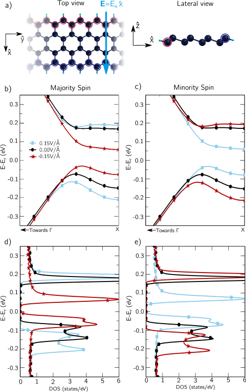
As graphene, stanene is characterized by a honeycomb lattice (with unit vector of Å), but with a buckled structure with two parallel planes of atoms separated by Å Zhu16 . The considered nanoribbon width is nm: for such a thin nanoribbon, a large exchange interaction between edges is expected, preserving magnetism at room temperature Jung09 ; Yazyev10 . While spin orbit coupling (SOC) is crucial for the appearance of topological spin-polarized edge states in topological insulators, in the anti-ferromagnetic configuration the spin polarization emerges due to the inter-edge exchange and SOC plays a minor role. In particular, for the studied system we have observed that the calculations including SOC have a negligible impact on the band-structure and the sensibility to the electric field is not modified.
In the absence of electric field, the stanene bandstructure for spin up and down is degenerate (Fig. 2b and c, black circles), with an energy bandgap of 0.25 eV. The states close to the conduction band minimum (CBM) and the valence band maximum (VBM) are localized at the edges of the nanoribbon, and according to the anti-ferromagnetic configuration, present opposite spin Xiong16 ; Nanoscale17 . By applying a positive transversal electric field, (Fig. 2a), the energy bandgap increases for spin up bands and decreases for spin down bands: opposite behavior occurs for negative . For example, for V/Å, the spin-down bandgap reduces to eV, and for spin-up increases to eV (Fig 2b and c).
As can be seen in Fig. 2d and e, the small curvature of the stanene bandstructure around the CBM and the VBM leads to corresponding peaks in the density of states (DOS). Coherently with Fig. 2b and c the spin-up and spin-down DOS have opposite dependence on . Eventually, for V/Å the material becomes a half metal (zero bandgap). A similar magnitude of the electric field is necessary to achieve half-metallicity in graphene, silicene, and germanene Son06 ; Wang13 . These values are, however, larger than the breakdown fields of practical dielectrics, and a device design sensitive to a small modulation of the bandgap is mandatory to take practical advantage of this effect in spintronics.
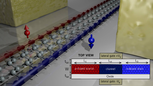
To this purpose, we propose a TFET structure where the stanene nanoribbon is embedded in SiO2, and sandwiched between two lateral metallic contacts, placed nm far from each nanoribbon edge (Fig. 3). The current flow is enabled by interband tunneling between the undoped-channel valence band (VB) and the doped-drain conduction band (CB), but - differently from a TFET - the switching current modulation is due to the modulation of the channel bandgap. The interband tunneling current is extremely sensitive to bandgap variations, so that with small electric fields it is possible to tune the alignment between the VB and the CB and consequently achieve large modulation of the spin-polarized current.
The considered nanoribbon has a length of nm. At its ends, we have assumed nm-long -/-doped regions, with acceptor/donor molar fractions equal to . The nm-long central region is the device channel. The two lateral gates are used to create a transversal electric field that, depending on its sign, allows to open/close the channel bandgap for each spin component.
In order to accurately study the performance of the proposed device, we have performed transport simulations solving self-consistently the three-dimensional Poisson equation, together with the open-boundary Schrödinger equation (see Methods). Spin-up and spin-down polarized currents () in the ballistic regime at room temperature ( K) have been calculated exploiting the Landauer’s formalism Landauer88 ; Buttiker90 .
In order to illustrate the working principle of the proposed device, we have depicted the density of states (DOS) as a function of the energy (refereed to the Fermi level at the source lead), and the position along the nanoribbon length (), for both spin-up and spin-down carriers (Fig. 4).
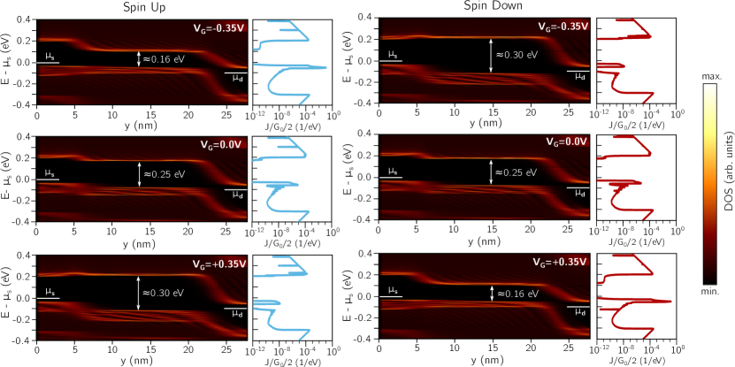
On the right of each DOS plot we have included the spectrum of the current density for the corresponding spin, normalized to half the conductance quantum () in semi-logarithmic scale. A drain-to-source voltage V and several values of are considered. The Fermi level at the source () and drain () leads are depicted together with the gap value at the channel. From the DOS colormap, one can easily recognize the CB and the VB, that correspond to two high-DOS stripes. The energy gap is also identified as a zero-DOS region between the CB and the VB. As can be seen, in the channel region ( nm nm) the bandgap width is modulated by , while it remains invariant at the source and drain regions where the influence of the gates is negligible. The device behavior is thus explained as follows: when V (Fig. 4 center panel) spin-down and spin-up carriers face equal barriers for inter-band tunneling and the current-density spectrum (normalized to ) does not show significant differences, and therefore the total current has no spin polarization. On the contrary, when V spin-up and spin-down carriers experience different channel interband tunneling bandgap and consequently the current has a spin polarization.
In particular, for V (Fig. 4 top panel), the bandgap for the spin-down states widens ( eV) whilst it closes ( eV) for spin-up states. As a consequence, when the channel bandgap is increased the inter-band (from the channel VB to the drain CB) tunneling probability is reduced, resulting in a decrease of the spin-down current, until only the thermionic components are visible. On the other hand, as the channel bandgap is reduced for spin-up states, the carriers from the -doped source VB fill the channel VB, and tunnel through the channel-VB-to-drain-CB thin barrier, notably increasing the tunneling current for this spin component, as shown by the current-density spectrum, and resulting in a highly spin-polarized total current. Symmetrically opposite behavior is observed for V (Fig. 4 bottom panel).
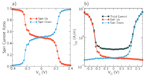
The spin-to-total current ratio as well as the total current and the spin-up and spin-down components are shown as a function of the applied gate voltage in Fig. 5, for V. The total current (grey squares) shows a symmetric behavior with a minimum at V, when current has no spin polarization, as spin-up (red circles) and spin-down (blue triangles) currents provide equal contribution. If a non-zero is applied, the symmetry is broken, and the total current becomes slightly spin-polarized with spin-up for and spin-down for . The spin polarization of the current increases with and achieves for V, and for V.
Discussion
We have theoretically demonstrated the electrical behavior of a device based on 2-D stanene, able to provide tunable spin-polarized current up to a polarizion of 98% with a small applied voltage on the controlling electrode. The proposed device is based on the modulation of the bandgap of narrow stanene nanoribbons and the edge-localized nature of the conduction and the valence band states. Taking advantage of this property, the device controls the interband tunneling currents through electric-field modulation of the energy bandgap, achieving a spin polarization as high as with electric field of 0.3 V/nm. We think that the proposed device might be useful to explore new concepts of spin injectors or filters, that are fundamental building blocks of spintronics.
Acknowledgements
Authors gratefully acknowledge the support from the Graphene Flagship Core 2 Contract No. 785219.
References
- (1) S. A. Wolf, D. D. Awschalom, R. A. Buhrman, J. M. Daughton, S. Von Molnar, M. L. Roukes, A.Y. Chtchelkanova, and D. M Treger, Spintronics: a spin-based electronics vision for the future, Science, 294, 1488 (2001).
- (2) D. D. Awschalom, and M. E. Flatté, Challenges for semiconductor spintronics, Nat. Phys., 3, 15 (2007).
- (3) C. Felser, G. H. Fecher, and B. Balke, Spintronics: a challenge for materials science and solid‐state chemistry, Ang. Chem. Int. Ed., 46, 668 (2007).
- (4) M. N. Baibich, J. M. Broto, A. Fert, F. N. Van Dau, F. Petroff, P. Etienne, G. Creuzet, A. Friederich, and J. Chazelas. Giant magnetoresistance of (001) Fe/(001) Cr magnetic superlattices, Phys. Rev. Lett., 61, 2472 (1988).
- (5) J. S. Moodera, L. R. Kinder, T. M. Wong and R. Meservey, Large magnetoresistance at room temperature inferromagnetic thinfilm tunnel junctions, Phys. Rev. Lett., 74, 3273 (1995).
- (6) Y. Xu, D. D. Awschalom, and J. Nitta. Handbook of spintronics. Springer Publishing (2016).
- (7) I. Zutic, J. Fabian, S. Das Darma Spintronics: fundamentals and applications, Rev. Mod. Phys., 76, 323 (2004).
- (8) X. L. Qi, and S. C. Zhang, Topological insulators and superconductors, Rev. Mod. Phys., 83, 1057 (2011).
- (9) M. N. Leuenberger, and D. Loss, Quantum computing in molecular magnets, Nature, 410, 789, (2001).
- (10) C. O. Avci, A. Quindeau, C. F. Pai, M. Mann, L. Caretta, A. S. Tang, M. C. Onbasli, C. A. Ross, and G. S. Beach, Current-induced switching in a magnetic insulator, Nat. Mat., 16, 309 (2017).
- (11) I. M. Miron, K. Garello, G. Gaudin, P. J. Zermatten, M. V. Costache, S. Auffret, S. Bandiera, B. Rodmacq, A. Schuhl, and P. Gambardella, Perpendicular switching of a single ferromagnetic layer induced by in-plane current injection, Nature, 476, 189 (2011).
- (12) L. Liu, C. F. Pai, Y. Li, H. W. Tseng, D. C. Ralph, and R. A. Buhrman, Spin-torque switching with the giant spin Hall effect of tantalum, Science, 336, 555 (2012).
- (13) M. Hosomi, H. Yamagishi, T. Yamamoto, K. Bessho, Y. Higo, K. Yamane, H. Yamada, M. Shoji, H. Hachino, C. Fukumoto, and H. Nagao, A novel nonvolatile memory with spin torque transfer magnetization switching: Spin-RAM, IEDM Technical Digest. IEEE International, 459 (2005).
- (14) G. Prenat, K. Jabeur, G. D. Pendina, O. Boulle, and G. Gaudin, Spintronics-based computing. Spin orbit torque RAM SOT-MRAM for high speed and high reliability applications, Springer Publishing, 145 (2015).
- (15) C. Tsang, R. E. Fontana, T. Lin, D. E. Heim, V. S. Speriosu, B. A. Gurney, and M. L. Williams, Design, fabrication and testing of spin-valve read heads for high density recording, IEEE Trans. on Magnetics, 30, 3801 (1994).
- (16) T. M. Hermann, W. C. Black and S. Hui, Magnetically coupled linear isolator, IEEE Trans. on Magnetics, 33, 4029 (1997).
- (17) W. J. Gallagher, and S. S Parkin. Development of the magnetic tunnel junction MRAM at IBM: From first junctions to a 16-Mb MRAM demonstrator chip, IBM J. Res. Dev., 50, 5 (2006).
- (18) S. Datta, and S. Das Darma, Electronic analog of the electro-optic modulator, App. Phys. Lett., 56, 665 (1990).
- (19) H. Ohno, D. Chiba, F. Matsukura, T. Omiya, E. Abe, T. Dietl*, Y. Ohno, and K. Ohtan. Electric-field control of ferromagnetism, Nature, 408, 944 (2000).
- (20) A. I. Khan, K. Chatterjee, B. Wang, S. Drapcho, L. You, C. Serrao, S. R. Bakaul, R. Ramesh, and S. Salahuddin, Negative capacitance in a ferroelectric capacitor. Nat. Mat., 14, 182 (2015).
- (21) H. Ohono, M. D. Styles, and B. Dieny, Spintronics, Proceedings IEEE, 104, 1782 (2016).
- (22) G. Y. Gao, and K. L. Yao, Antiferromagnetic half-metals, gapless half-metals, and spin gapless semiconductors: The D03-type Heusler alloys, App. Phys. Lett., 103, 232409 (2013).
- (23) F. J. Jedema, A. T. Filip, and B. J. Van Wees, Electrical spin injection and accumulation at room temperature in an all-metal mesoscopic spin valve, Nature, 410, 345 (2001).
- (24) R. A. De Groot, F. M. Mueller, P. G. Van Engen, and K. H. J. Buschow, New class of materials: half-metallic ferromagnets, Phys. Rev. Lett., 50, 2024 (1983).
- (25) Y-W. Son, M. L. Cohen, and S. G. Louie, Half-metallic graphene nanoribbons, Nature, 446, 342 (2006).
- (26) X. L. Wang, Proposal for a new class of materials: spin gapless semiconductors, Phys. Rev. Lett., 100, 156404 (2008).
- (27) S. Ouardi, G. H. Fecher, C. Felser, and J. Kübler, Realization of spin gapless semiconductors: the Heusler compound Mn2CoAl, Phys. Rev. Lett., 110, 100401 (2013).
- (28) K. S. Novoselov, A. K. Geim, S. V. Morozov, D. Jiang, Y. Zhang, S. V. Dubonos, I. V. Grigorieva, and A. A. Firsov, Electric field effect in atomically thin carbon films, Science, 306, 666 (2004).
- (29) S. Roche, J. Akerman, B. Beschoten, J. C. Charlier, M. Chshiev, S. P. Dash, B. Dlubak, J. Fabian, A. Fert, M Guimaraes, and F. Guinea, Graphene spintronics: the European Flagship perspective, 2D Materials, 2, 030202 (2015).
- (30) W. Han, R. K. Kawakami, M. Gmitra, and J. Fabian, Graphene spintronics, Nat. Nano., 9, 794 (2014).
- (31) J. H. Garcia, M. Vila, A. W. Cummings, and S. Roche, Spin transport in graphene/transition metal dichalcogenide heterostructures, Chem. Soc. Rev., 47, 3359 (2018).
- (32) D. Pesin, and A. H. Macdonald, Spintronics and pseudospintronics in graphene and topological insulators, Nat. Mat., 11, 409 (2012).
- (33) G. Gao, G. Ding, J. Li, K. Yao, M. Wu, and M. Qian, Monolayer MXenes: promising half-metals and spin gapless semiconductors, Nanoscale, 8, 8986 (2016).
- (34) Y. Nie, M. Rahman, P. Liu, A. Sidike, Q. Xia, and G. H. Guo, Room-temperature half-metallicity in monolayer honeycomb structures of group-V binary compounds with carrier doping, Phys. Rev. B, 96, 075401 (2017).
- (35) M. Ashton, D. Gluhovic, S. B. Sinnott, J. Guo, D. A. Stewart, and R. G. Hennig, Two-dimensional intrinsic half-metals with large spin haps, Nano Lett., 17, 5251 (2017).
- (36) E. J. Kan, Z. Li, J. Yang, and J. G. Hou, Half-metallicity in edge-modified zigzag graphene nanoribbons, J. Ame. Chem. Soc., 130, 4224 (2008).
- (37) O. V. Yazyev, and L. Helm, Defect-induced magnetism in graphene, Phys. Rev. B, 75, 125408 (2007).
- (38) J. Bundesman, M-H. Liu, I. Adagideli, K. Richter, Spin conductance of diffusive graphene nanoribbons: A probe of zig-zag edge magnetization, Phys. Rev. B, 88, 195406 (2013).
- (39) N. Tombros, C. Jozsa, M. Popinciuc, H. T. Jonkman, and B. J. Van Wees, Electronic spin transport and spin precession in single graphene layers at room temperature, Nature, 448, 571 (2007).
- (40) W. Han, K. Pi, K. M. McCreary, Y. Li, J. J. Wong, A. G. Swartz, and R. K. Kawakami, Tunneling spin injection into single layer graphene, Phys. Rev. Lett., 105, 167202 (2010).
- (41) A. Molle, J. Goldberger, M. Houssa, Y. Xu, S. C. Zhang, and D. Akinwande, Buckled two-dimensional Xene sheets, Nat. Mat., 16, 163 (2017).
- (42) P. Vogt, P. de Padova, C. Quaresima, J. Avila, E. Frantzeskakis, M-C. Asensio, A. Resta, B. Ealet, and G. Le Lay, Silicene: compelling experimental evidence for graphene-like two-dimensional silicon, Phys. Rev. Lett., 108, 155501 (2012).
- (43) M. E. Davila, L. Xian, S. Cahangirov, A. Rubio, and G. Le Lay, Germanene: a novel two-dimensional germanium allotrope akin to graphene and silicene, New Journal Phys., 16, 095002 (2014).
- (44) F. F Zhu, W. J. Chen, Y. Xu, C. L. Gao, D. D. Guan, C. H. Liu, D. Qian, S. C. Zhang, and J. F. Jia, Epitaxial growth of two-dimensional stanene. Nat. Mat., 14, 1020 (2015).
- (45) T-C. Wang, C-H. Hsu, Z-Q. Huang, F-C. Chuang, W-S. Su, and G-Y. Guo, Tunable magnetic states on the zig-zag edges if hydrogenated and halogenated group-IV nanoribbons, Sci. Rep., 6, 39083 (2016).
- (46) W. Xiong, C. Xia, Y. Peng, J. Du, T. Wang, J. Zhang, Y. Jian, Spin-orbit coupling effects on electronic structures in stanene nanoribbons, Phys. Chem. Chem. Phys., 18, 6534 (2016).
- (47) Y. Wang, J. Zheng, Z. Ni, R. Fei, Q. Liu, R. Quhe, C. Xu, J. Zhou, Z. Gao, and J. Lu, Half-metallic silicene and germanene nanoribbons: towards high-performance spintronics device. Nano, 7, 1250037 (2012).
- (48) J. Jung, T. Pereg-Barnea, and A. H. MacDonald, Theory of interedge superexchange in zig-zag edge magnetism, Phys. Rev. Lett., 102, 227205 (2009).
- (49) O. V. Yazyev, Emergence of magnetism in graphene materials and nanostructures, Rep. Prog. Phys., 73, 056501 (2010).
- (50) P. Giannozzi, S. Baroni, N. Bonini, M. Calandra, R. Car, C. Cavazzoni, D. Ceresoli, G. L. Chiarotti, M. Cococcioni, I. Dabo, A. Dal Corso, S. de Gironcoli, S. Fabris, G. Fratesi, R. Gebauer, U. Gerstmann, C. Gougoussis, A. Kokalj, M. Lazzeri, L. Martin-Samos, N. Marzari, F. Mauri, R. Mazzarello, S. Paolini, A. Pasquarello, L. Paulatto, C. Sbraccia, S. Scandolo, G. Sclauzero, A. P. Seitsonen, A. Smogunov, P. Umari and R. M. Wentzcovitch, QUANTUM ESPRESSO: a modular and open-source software project for quantum simulation of materials, J. Phys.: Cond. Matt., 21, 395502 (2009).
- (51) J. P. Perdew, K. Burke, and M. Ernzerhof, Generalized gradient approximation made simple, Phys. Rev. Lett., 77, 3865. (1996).
- (52) Standard Solid State Pseudopotentials (SSSP), http://www.materialscloud.org/sssp, (2017).
- (53) E. G. Marin, D. Marian, G. Iannaccone, and G. Fiori, First principle investigation of Tunnel FET based on nanoribbons from topological two-dimensional material, Nanoscale, 9, 19390 (2017).
- (54) S. Datta, Nanoscale device modeling: the Green’s function method, Superlatt. Microstruc., 28, 253 (2000).
- (55) E. G. Marin, M. Perucchini, D. Marian, G. Iannaccone, G. Fiori, Modeling of electron devices based on two-dimensional materials, IEEE Trans. Elec. Dev., 85, 4167 (2018).
- (56) Nano TCAD ViDES. 2017, available at: http://vides.nanotcad.com/vides/.
- (57) N. Marzari, A. A. Mostofi, J. R. Yates, I. Souza, D. Vanderbilt, Maximally localized Wannier functions: theory and applications, Rev. Mod. Phys., 84, 1419 (2012).
- (58) G. Pizzi, M. Gibertini, E. Dib, N. Marzari, G. Iannaccone, and G. Fiori, Performance of arsenene and antimonene double-gate MOSFETs from first principles, Nat. Comm., 7, 1 (2016).
- (59) R. Landauer, Spatial variation of currents and fields due to localized scatterers in metallic conduction, IBM J. Res. Dev., 32, 306 (1988).
- (60) M. Buttiker, Scattering theory of thermal and excess noise in open conductors, Phys. Rev. Lett., 65, 2901 (1990).