Light-matter interaction of a quantum emitter near a half-space graphene nanostructure
Abstract
The Purcell factor and the spontaneous emission spectrum of a quantum emitter (QE) placed close to the edge of a graphene half-space nanostructure is investigated, using semi-analytical methods at the electrostatic regime. The half-space geometry supports an edge and a bulk surface plasmon (SP) mode. The Purcell factor of the QE is enhanced over eight orders of magnitude when its emission energy matches the resonance energy modes, for a specific value of the in-plane wave vector, at a separation distance of nm. The different transition dipole moment orientations influence differently the enhancement factor of a QE, leading to large anisotropic behavior when positioned at different places above the half-space geometry. The field distribution is presented, showing clearly the excitation of the SP modes at the edge of the nanostructures. Also, we present the spontaneous emission spectrum of the QE near the half-space graphene nanostructure and show that strong light-matter coupling may emerge. When a QE with a free-space lifetime of ns is placed at a distance of nm away from the edge of the graphene half-space, a Rabi splitting of eV is found. Our contribution can be used for designing future quantum applications using combination of QEs and graphene nanostructures.
I INTRODUCTION
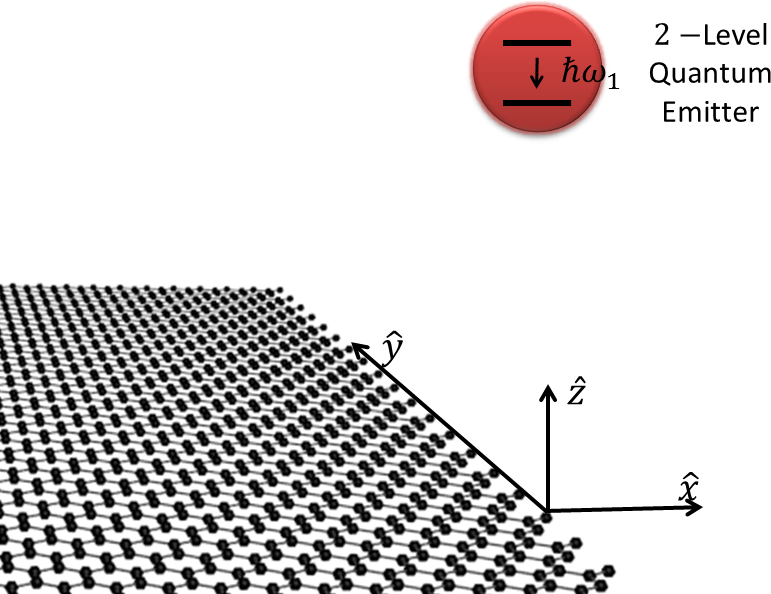
The polariton modes, which are collective hybrid light-matter modes, open the opportunity to control light at the nanoscale Basov16a ; Low2017 . Among the various hybrid modes the most studied ones are the surface plasmon (SP) modes. The SP are hybrid modes of the electromagnetic field and the conduction band electrons, which are confined in the interface between a metal and a dielectric, where they propagate along it and are confined in the perpendicular dimension. Graphene is a material with higher optical and mechanical properties that is also expected to replace noble metals (Au and Ag mainly) in photonics applications based on SP modes, due to lower material losses, at the mid- to far- infrared parts of the spectrum Low2014a ; GarciadeAbajo2014 . The graphene SP excitation modes are in the infrared part of the spectrum Koppens2011 , and are tunable, controlled by electric field gating, doping or multilayer stacking. Also, the fabrication capabilities and detection technologies developed over the last decade open new routes for manipulating the light to the extreme for building sophisticated applications Fang2013 ; Tielrooij2015 .
The SP modes can be excited by different ways, such as plane wave, fast electrons or localized sources, like quantum emitters (QEs), which have active properties GarciadeAbajo2010a . For infinite planar graphene nanostructures special techniques are needed to excite the SP modes due to the large miss-match in the momentum between them and the incoming light Nikitin2014 . On the same time localized scatterers have been used to launch surface plasmon modes to localized and extended graphene nanostructures, like Au particles Alonso2014 or metallic tips Chen2012 ; Fei2011 , where the scattered field can provide the high wave vector components needed to excite the SP modes. Novel experimental techniques have also been used to launch the SP modes and also to measure the fields amplitude and phase Gerber2014 . However, these techniques are limited by the excitation wavelength and do not operate at the near infrared part of the spectrum.
Surface polariton modes, of any kind plasmon, exciton or phonon, can confine light at the extreme Basov16a ; Low2017 thus opening new routes for detection application, but also for applications for novel quantum technologies. For these all-optical devices various processes need to be handled on-chip, where the basic idea is to be able to transfer to the chip information and extract from the chip its response. The information can be transmitted/extracted to/from this chip by a QE. A QE is described as a two-level system, approaching various physical systems, such as atoms, molecules, quantum dots, quantum wells and color centers Baranov2018 . So, we need to fully understand how a QE interacts with a device at its boundary.
We note that the interaction of QEs with graphene monolayers and graphene nanostructures, like graphene waveguides and nanodisks, is a topic of active research Koppens2011 ; Cox12a ; Manjavacas12a ; Forati14a ; Sun2014 ; Karanikolas2015 ; Karanikolas16b ; Cuevas2016 ; Rivera16a ; Chang17a ; Sun2017 ; Cuevas18 ; Sloan18a ; Karanikolas18a ; Zhang18a ; Sanders18a ; Fang18a ; Cox18a ; Cuevas19a ; Zeng19a ; Zhang19a . However, the interaction of a QE with a graphene half-space geometry, to the best of our knowledge, remains unexplored. Thus, here we investigate the spontaneous emission (SE) properties of a QE placed near the edge of a graphene half-space geometry, which is depicted at Fig. 1. Furthermore, we study the edge and bulk SP modes and present the SP field intensity launched by a QE. The QE/graphene half space geometry interaction is described using the non-Hermitian quantum description of light-matter interaction Dung2000 . In the heart of this theory is the knowledge of the electromagnetic (EM) Green’s tensor Nanoopticsbook , which has a classical interpretation, it gives the electromagnetic response of the geometry under consideration to a point-like dipole excitation. Here, we calculate this quantity in the electrostatic regime, since the graphene half-space geometry can support SP modes up to the near infrared part of the spectrum Fetter1986 ; Wang2011 , and extract from this the Purcell factor.
The Purcell factor of the QE is the main quantity of interest in the weak light-matter coupling regime, as it quantifies the change of the SE rate of the QE. We find that the Purcell factor takes very large values, larger than , near the edge of the graphene half-space geometry. We also show that when the QE/graphene half-space nanostructure separation is small, we enter the strong light-matter coupling regime Baranov2018 ; Vanvlack12a ; Tejedor14 ; Hakami14 ; Li16a ; Thanopulos2017 ; Rousseaux18a ; Karanikolas19a . At this regime the combined system QE/half-space geometry coherently exchange energy between its two constituent elements. The strong coupling regime appears as a splitting, the Rabi splitting, in the SE spectrum of the QE near the graphene half-space nanostructure.
We start in Sec. II.1 by presenting the mathematical frame under which we calculate the Purcell factor and the SE spectrum of a QE, using the non-Hermitian description of the light-matter interaction. In Sec. II.2, where the dispersion relation, the propagation length and the penetration depth of the graphene half-space are analyzed, we identify the edge and bulk SP modes. In Sec. III we present the Purcell factor of a QE located at the edge of the graphene half-space nanostructure placed at the plane, while varying its emission energy and the in-plane wave vector value, for the and transition dipole moments of the QE. Also, for specific values of the emission energy and of the wave vector we vary the the position of the QE along the nanostructure, in order to probe the behavior of the dipole orientation. The Green’s tensor amplitude, which is connected with the EM field, created by a QE is also presented for the edge and bulk SP modes. This section is finalized by presenting the SE spectrum of a QE, placed at the edge of the graphene half-space geometry. A pronounced Rabi splitting is achieved, showing that the QE/half-space interaction operates at the strong coupling regime. Sec. IV concludes our findings. In Appendix A we present an expansion method, to a known set of functions, to calculate the Green’s tensor for the case of the graphene half-space geometry at the electrostatic limit. In Appendix B we present the surface conductivity of graphene, that gives its optical response.
II Theoretical description of the light-matter interactions
II.1 Purcell factor and spontaneous emission rate
As localized sources we consider QEs which are approximated as two-level systems. The ground state of the QE is and the excited state is . The transition frequencies from the excited to the ground state and the dipole matrix element are denoted as and , respectively. An initially excited QE interacts with its environment through the electromagnetic field and relaxes from its excited state to the ground state by emitting a photon (radiative relaxation path) or exciting any of the dressed states supported by its environment. For the case investigated here the dressed states will be the edge and bulk SP modes. The initial state of the system is denoted as , where the QE is in the excited state and the electromagnetic field is in its vacuum state. The QE will relax to the final state of the entire system . By applying Fermi’s golden rule and summing over all final states, the expression for the relaxation rate is , where is a unit vector along the direction of the transition dipole moment, , and is the EM Green’s tensor.
For the case of graphene half-space the Green’s tensor for a QE that his transition dipole moment is along has the form:
| (1) |
where the QE is placed at , above the edge of the graphene half-space, and are expansion coefficients that depend on the position of the QE. For the case we have a QE with a -oriented transition dipole moment, the EM Green’s tensor has the form:
| (2) |
In the above expressions we define , more details for the calculation are given in Appendix A.
Using Eqs. (1) and (2) we obtain the Purcell factor of the QE
| (3) |
which shows in the weak coupling regime if the SE rate of the QE is enhanced or inhibited in the presence of the graphene half-space geometry in respect to the free space case. Here, is the permittivity of the host medium and is the Einstein -coefficient, with . We stress that we deal with the near field regime of the QE, which means that the QE - graphene half-space geometry separation is much smaller than the emission wavelength of the QE, .
For the strong coupling a different approach is needed. We need to describe the full problem where the strength of energy exchange between the QE/nanostructure combined system is determined through the spectral density , which also depends on the Purcell factor, and has the expression Vanvlack12a ; Tejedor14 ; Hakami14 ; Li16a ; Thanopulos2017 ; Rousseaux18a ; Karanikolas19a
| (4) |
with . We observe that the higher the Purcell factor the stronger the coupling of the QE with its environment. Also, the value of the dipole strength is very important for approaching the strong coupling limit, the higher its value the less enhancement of the Purcell factor is needed Baranov2018 . The light emitted spectrum of the QE is given by where, after carrying out the calculations, the full expression has the form Vanvlack12a ; Hakami14 ; Karanikolas19a
| (5) |
Here, is the position of the signal detection, is the position of the QE and is the emission frequency.
II.2 Analysis of the surface plasmon modes
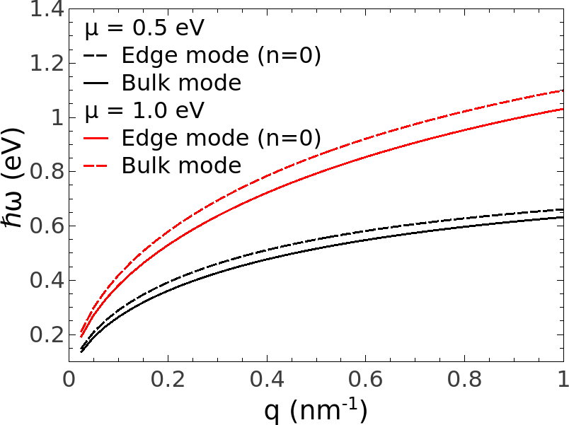
In Fig. 2a we present the dispersion relation of the half-space geometry, where we observe that two modes are supported, the edge and the bulk. To find these resonance frequencies, for each wave number, we set to zero the external excitation to Eq. (16) and we numerically solve the equation
| (6) |
where are the geometric eigenmodes which are solutions of the equation and once and for all are determined for the half space geometry. The exact forms of the and matrices are given in the Appendix A, and are obtained via an expansion over the Laguerre polynomials Fetter1986 . The optical response of graphene is described through its surface conductivity , where more details are given in Appendix B. The is connected to the edge mode and the corresponds to the bulk mode. The modes for they have the same dispersion relation as the mode and are physically connected with the fact that the bulk mode is continuous, modified from the bulk mode of the infinite planar graphene sheet Karanikolas2015 . In Fig. 2a we observe that the bulk SP mode energy, , is blue shifted for any given value of the wave vector compared to the edge SP mode. All branches are well below the free space light-line, which is very close to the axis of Fig. 2a. Furthermore, we observe that by increasing the value of the chemical potential the dispersion relations for the edge and bulk modes is blue-shifted a clear indication of the capabilities offered by graphene for designing tunable photonic applications.
The SP mode is characterized by the propagation length, , and the penetration depth, , supported by the graphene half-space geometry. The propagation length is connected with the distance along the graphene half-space geometry that the SP mode intensity propagates until attenuated to value and it can be defined as Christensen2012 , where ps is the relaxation time of the surface conductivity, in Eq. (30), that in turn is connected with the SP modes to acquire a finite lifetime. The relaxation time, , is influenced by several factors, such as collisions with impurities, coupling to optical phonons, finite-size and edge effects. Here, is the group velocity of the SP modes and is given by the slope of the dispersion relations for the edge and bulk modes. The penetration depth is connected with the extend of the SP mode in the direction. It physically shows with how effectively can a QE excite the SP mode by coupling with his near field regarding the QE’s position. Large penetration depths can be used to effectively couple a QE at larger distances. The penetration depth is defined as , where Karanikolas2015 .
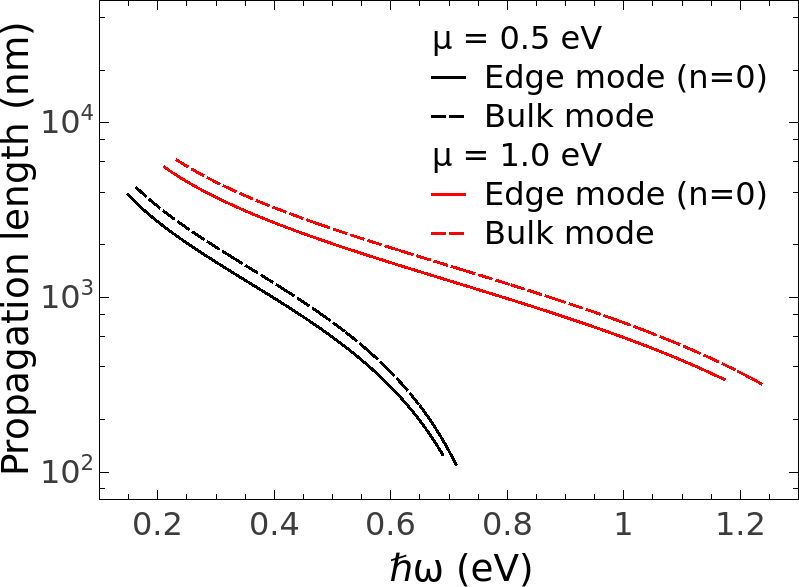
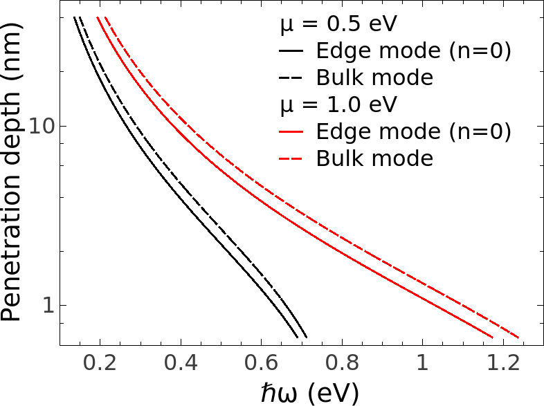
In Fig. 2b we present the propagation length, , for varying energy , considering two values for the chemical potential eV and eV. We have two propagation lengths and for the edge and the bulk SP modes, respectively. We observe that for any given energy, , the propagation length for the bulk mode is larger than the propagation length for the edge mode, for both chemical potential values. Furthermore, as the energy of the mode is increased, the propagation lengths and decrease rapidly, because the SPs have sufficient energy to generate electron-hole pairs and the dispersion relation is dominated by the interband contributions on the surface conductivity . Moreover, as the chemical potential value is increased the propagation lengths of edge, , and bulk modes, , are also increased. In this case, the SP modes acquire more energy for propagating along the half-space geometry. In Fig. 2c we observe a similar behavior for the penetration depth, for the edge, , and bulk, , modes, with the propagation length, regarding the tunability and the reduction of their value for increasing energy. Also, the edge mode is more tightly confined to the graphene half-space geometry than the bulk mode, since for any given energy for the same chemical potential values. The main difference between the two lengths is that the propagation lengths are around two order of magnitudes larger that the penetration depths, meaning the the SP modes are tightly confined to the graphene half-space geometry and are able to propagate several hundreds of nanometers until being attenuated. This properties are important for designing future practical applications using graphene as a building block.
III Emission properties at the weak and strong coupling regimes
In this section we focus on the SE properties of a QE in the presence of the graphene half-space geometry. High values of the Purcell factor are presented. The QE can efficiently excite edge and bulk SP modes by relaxing at the edge of the graphene half-space geometry. Also, strong light-matter coupling is presented in certain cases.
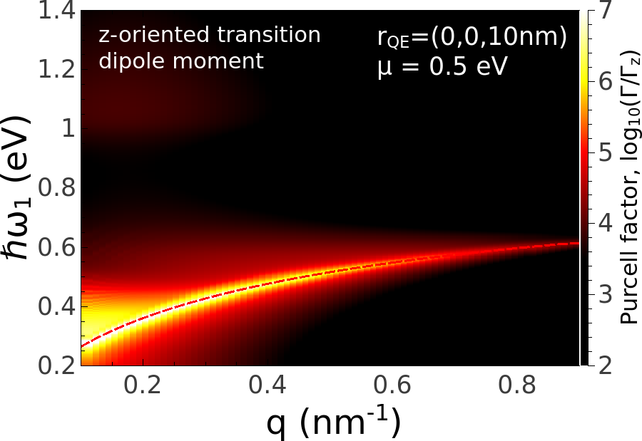
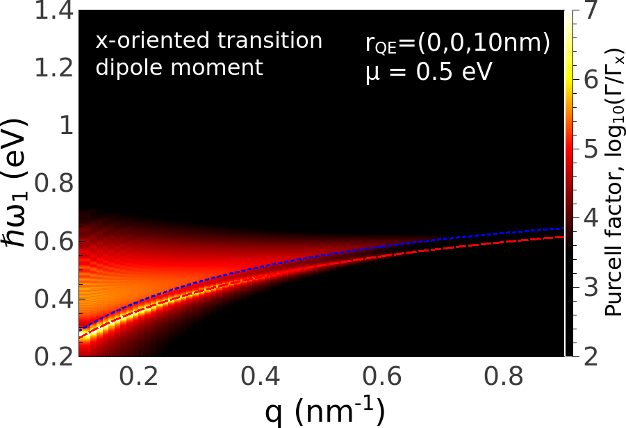
In Fig. 3 we present a contour plot of the logarithm of the Purcell factor of a QE, placed at , varying , for different values of the in-plane wave vector, . The chemical potential of the graphene half-space is eV and the position of the QE is exactly at the edge of the graphene half-space nanostructure, see Fig. 1. Two different transition dipole moment orientations of the QE are considered, in (a) -oriented and in (b) -oriented. We observe that for a QE with -oriented dipole moment can couple efficiently with the edge resonance mode, . Thus, for these values the Purcell factor increases above orders of magnitude in the presence of the graphene half-space structure. Also, for the specific QE position, the near field of the QE can efficiently couple with the bulk SP mode, , when its transition dipole moment is oriented along . Hence, the enhancement of the Purcell factor is above orders of magnitude compared to the free space value. For both orientations, we observe that for increasing the value of the in-plane wave vector the Purcell factor of the QE drops. This has a physical explanation connected with the SP penetration depth where for the higher mode the SP field is more confined to the graphene half-space making it more difficult for the QE to efficiently excite the SP modes. Thus, for exciting the higher modes the QE needs to be placed very close to the nanostructure to provide the necessary high in-plane wave vector component values.
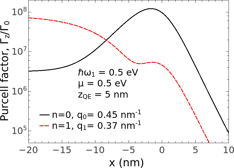

In Fig. 4 we present the Purcell factor of a QE when we vary its position above the graphene half-space geometry, with chemical potential of eV. The QE position is at and the emission energy value eV, matching the resonance wave vectors , and at and , respectively. The wave vector is connected with the edge SP mode and the is connected with the bulk mode. Two transition dipole moment orientations of the QE are considered, along in Fig. 4a and along in Fig. 4b. We observe in Fig. 4a that the enhancement of the Purcell factor has the largest value for the edge SP mode compared to the bulk mode, more than one order of magnitude difference, when the QE is close to the edge of the graphene half-space geometry. As the position of the QE is moved away from the edge of the graphene half-space to the bulk, , the edge mode contribution to the Purcell factor of the QE is reduced and the bulk SP mode is enhanced, that is the main relaxation path of the QE. Also, when the QE is placed out of the extend of the half space geometry, , the Purcell factor rapidly drops as we increase the distance, for a QE with a transition dipole moment along .
In Fig. 4b we observe that when the transition dipole moment of the QE is oriented along the Purcell factor is less enhanced right above the edge of the graphene half-space geometry for the mode, which means that an oriented QE cannot excite efficiently the edge SP mode right above the edge. As the QE is moved towards the bulk of the graphene structure, , we observe that the Purcell factor for the edge mode is peaked at around nm. At this position due to the transition dipole moment orientation the QE can efficiently excite the edge SP mode. Increasing further the distance from the edge of the half-space geometry the Purcell factor drops for the edge mode due to the decoupling of the near field of the QE to the edge SP mode. At these distances the bulk mode dominates, that is the main path of relaxation for the excited QE. In striking contrast to the oriented transition dipole moment of the QE, when the orientation is considered the Purcell factor is enhanced when the QE is placed away of the half-space geometry, , and is peaked at a distance of nm. Thus, when the transition dipole moment of the QE is considered the edge SP mode can be efficiently excited by placing a QE not exactly at the edge, but still close to the edge, of the graphene half-space geometry.
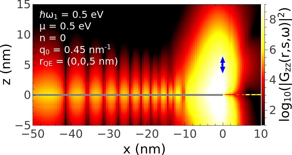
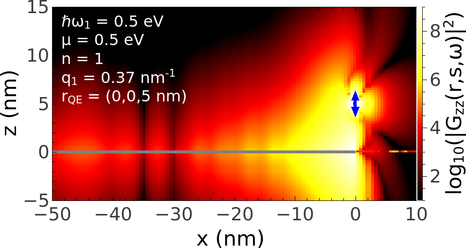
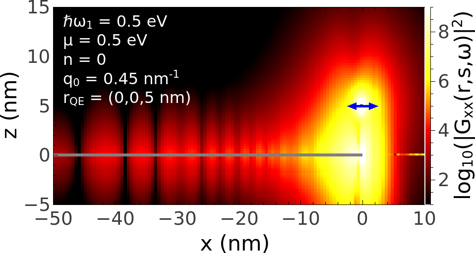
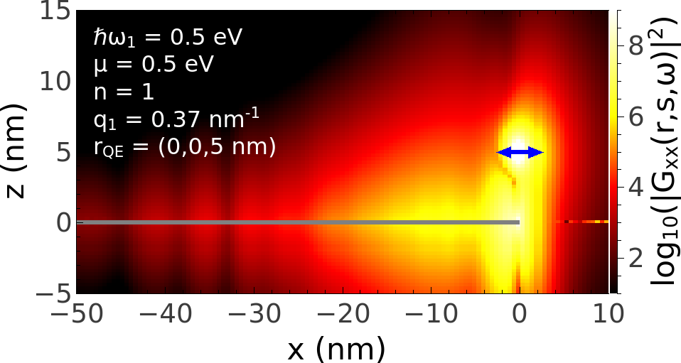
For better understanding the coupling of the QEs with the graphene half space geometry, in Fig. 5 we present a contour plot of the logarithm of the absolute value of the Green’s tensor, , created by a QE, which is placed at , at the plane in the presence of the graphene half-space nanostructure. Two different transition dipole moment orientations of the QE are considered, -oriented at Figs. (5a), (5b) and -oriented at Figs. (5c), (5d). The chemical potential of graphene half-space is eV and the emission energy of the QE is eV. Two resonance wave vectors are considered and at Figs. (5a), (5c) and (5b), (5d), respectively. All color map scales in Fig. 5 are the same, allowing the reader for a direct comparison.
In Fig. 5a we observe that a QE with a transition dipole moment oriented along can launch an edge SP mode, , on the graphene half-space geometry efficiently. We observe that the SP mode is confined to the graphene sheet tightly. The emission energy of the QE is eV (nm) much larger than the penetration depth of the SP field nm, as seen in Fig. 2c, which matches the field extend observed in Fig. 5a. As , a three orders of magnitude confinement of light is observed, in the perpendicular direction. Moreover, as the distance from the edge towards the bulk graphene is increased the field intensity drops, and the field is dissipated due to the materials losses, an effect that is connected with the propagation length of the edge SP mode, where nm. When the bulk resonance mode is considered, for and , in Fig. 5b we observe that the field intensity is reduced, compared to the edge mode . Thus, the discontinuity of the graphene half-space geometry can be used to launch an edge SP mode at the edge, that is extremely confined on the sheet while it can travel hundreds of nanometers with large field values, which potentially can be used to couple other nearby QEs or nanostructures.
In Fig. 5c we present a contour plot of the field created by a oriented transition dipole moment QE, which is placed exactly at the edge of the graphene half-space geometry, . As someone would expect from the Purcell factor enhancement of Fig. 4b, when the QE is placed at the edge of the half space is only poorly coupled to the edge SP mode, , thus the field distribution is less profound than when a oriented transition dipole moment is considered. Nevertheless, we can see that the SP modes can be efficiently launched, although their strength is smaller by two orders of magnitude compared with the case a oriented QE is considered (Fig. 5a). When the in-plane wave vector matches the bulk mode, , the field further drops due to the poor coupling with the bulk mode. The main message obtained from Fig. 5 is that when a QE is placed at specific areas of interest can excite SP modes, which can enhance the Purcell factor and create large field enhancements. This control is active from the part of the QE, while for the case where a metallic tip is used it cannot launch SP modes with an arbitrarily small wave number due to the non-zero tip radius Fei2011a .
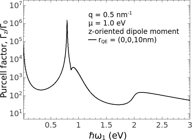
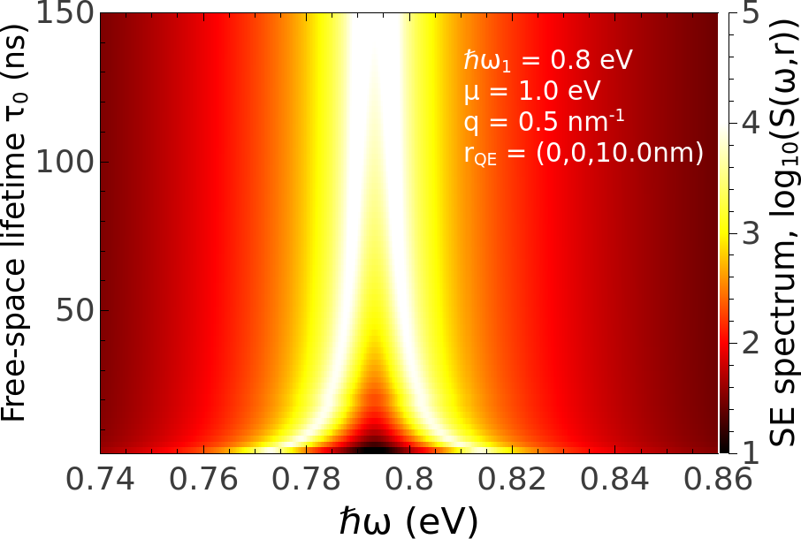
From the analysis up to now it has become clear that the presented enhancements of the Purcell factor of a QE are very large and thus the combined interaction QE/half-space nanostructure may enter in the strong coupling regime. In Fig. 6a we present the Purcell factor of the QE placed above the graphene half-space geometry edge, at with a oriented transition dipole moment. The graphene is kept at a chemical potential value of eV and the in-plane wave vector has a value of . We observe that at eV the Purcell factor becomes above . As we have already analyzed the Purcell factor is due to the excitation of the edge mode supported by the graphene half-space nanostructure.
From Eq. 4 it is clear that the value of the spectral density, for specific Purcell factor, depends on the free-space SE rate of the QE. The chemical potential of the graphene is eV and the in-plane wave vector is . In Fig. 6b we present a contour plot of the logarithm of the SE spectrum of the QE near the graphene half-space nanostructure, Eq. 5, for different free-space lifetimes of the QE, . The transition energy from the excited to the ground state of the QE is at eV (nm) which matches the highest value of the enhancement of the SE rate of the QE, presented in Fig. 6b. We observe that for the free-space lifetime value ns (typical for quantum dots) there is a Rabi-splitting in the emission spectrum of the combined system which has a value of eV. As the value of the free-space lifetime, , is increased the splitting drops and at free-space lifetimes above ns disappears and there is a transition from the strong to the weak coupling regime. Reducing the separation between the QE and the graphene half space will increase the Purcell factor enhancement, thus increasing the Rabi splitting. The same outcome we would have if we had considered different QEs with smaller lifetimes .
IV Conclusions
In this article we investigated the SE properties of a QE near a graphene half-space nanostructure in the weak and strong coupling regimes. A semi-analytical method was used to calculate the Green’s tensor at the electrostatic limit for the graphene half-space geometry, where an expansion over Laguerre polynomials was applied. The graphene half-space geometry supports edge and bulk SP modes, where by changing the value of the chemical potential we can tune their properties, namely, the dispersion relation , the propagation length , and the penetration depth of the edge and bulk SP modes, for and , respectively.
We showed that when a QE is placed close to the edge of the half-space geometry can efficiently excite the edge SP mode, and the Purcell factor can take significant values. Different transition dipole moments give different response to the enhancement of the Purcell factors. When the QE has a transition dipole moment orientation then the Purcell factor takes values larger than , when the QE is placed at nm away from the graphene edge. Once the QE is placed out of the surface of the graphene half-space, , then a QE with an transition dipole moment orientation dominates over a oriented one, coupling more efficiently to the edge SP mode.
Furthermore, we showed that the QE when placed at the edge of the graphene half-space geometry can launch edge and bulk SP modes without the need to use tip-metallic excitation and having access to really high wave vector values at high energies, relative to the chemical potential value . For all-optical applications based on two dimensional materials this is quite important as someone can efficiently transmit or extract information from the device to the environment using QEs.
Finally, the Purcell factor enhancement of the QE can reach large values and also has narrow spectral response, thus the interaction between the QE/graphene half-space nanostructure enters the strong coupling regime. Rabi splitting about eV is observed for a free space lifetime of ns, placed at a distance of nm above the graphene edge. The free-space emission energy is eV close to the telecommunication wavelength nm, a wavelength range that is very important for various applications.
As a next step in a similar line of research we will investigate the strong coupling regime of the interaction between a pair of QE placed in the vicinity of the graphene half-space geometry in the strong coupling regime. This will be important for further understanding how a practical quantum application can operate.
Appendix A eigenfrequencies and eigenfunctions of the electrostatic potential
In this Appendix we present a method to calculate the Green’s tensor for the graphene half-space geometry in the electrostatic limit. The electrostatic potential is found by solving the Poisson equation:
| (7) |
where is the dielectric permittivity and is the charge distribution due to the electrons provided by the graphene half space. Through out this paper we consider a constant value for the dielectric permittivity . This electrostatic problem has an obvious symmetry along the axis. Thus, we can write the potential and the charge density as: and . For and taking a Fourier transformation of Eq. (7) we extract the following differential equation:
| (8) |
which has solutions of the form . Applying the relevant boundary conditions, that the potential is continuous and its normal derivative has a discontinuity of the form:
| (9) |
the unknown coefficients have the form . Hence, the induced field is given by the expression:
| (10) |
where the kernel of the integral is given by the expression
| (11) |
We continue using Ohm’s law, , and the continuity equation, , to find the expression
| (12) |
where we have reintroduced . is the Green’s function, which is solution of the equation
| (13) |
on the interval and boundary condition
| (14) |
The solution of Eq. (13) has the form
| (15) |
At we have to solve the following integral equation:
| (16) |
where and is the external excitation created by a pseudo-potential. The only unknown quantity in the above equation is the charge density , to proceed we will transform the integral Eq. (16) to a matrix equation by expanding the surface charge density, , using Laguerre polynomials
| (17) |
where is the set of coefficients that they need to be determined, are the Laguerre polynomials which satisfy the following orthogonality condition
| (18) |
Using the above expansion, the orthogonality condition, we get the following matrix problem
| (19) |
where is a column vector where its elements are the expansion coefficients , are the expansion coefficients of the dipole source with a dipole orientation and they are given from the expression
| (20) |
when a point dipole source oriented along is considered, and
| (21) |
when the transition dipole moment is along . The elements of the matrices and are given by the expressions
| (22) |
and
| (23) |
respectively Fetter1986 .
The induced part of the pseudopotential is given by the expression
| (24) |
where all the lengths are normalized to the in-plane wave vector . Also, we have used the integral relation
| (25) |
The induced electrostatic Green’s tensor is given by the expression
| (26) |
Then, the Green’s tensor has the form
| (27) |
which is connected with the component of the electric field created by a dipole source oriented along , and
| (28) |
which is connected with the component of the electric field created by a dipole source oriented along .
Appendix B Graphene conductivity
The optical response of graphene is given by the value of the in-plane conductivity, , in the random phase approximation Jablan2009 ; Falkovsky2008 . This quantity is mainly determined by electron-hole pair excitations, which can be divided into intraband and interband transitions. It depends on the chemical potential , the temperature , and the scattering energy values as
| (29) |
where the intraband and interband contributions are given by Wunsch2006 ,
| (30) |
| (31) |
The intraband term describes a Drude model response, corrected for scattering by impurities through a term containing , the relaxation time. Throughout this paper we consider room temperature and a value of the relaxation time of and we vary the value of chemical potential, Novoselov2004 .
References
- (1) D. N. Basov, M. M. Fogler, and F. J. G. de Abajo, Science 354, aag1992 (2016).
- (2) T. Low, A. Chaves, J.D. Caldwell, A. Kumar, N.X. Fang, P. Avouris, T.F. Heinz, F. Guinea, L. Martin-Moreno, F. Koppens,Nature Mat. 16, 182 2017.
- (3) T. Low and P. Avouris, ACS Nano 8, 1086 (2014).
- (4) F. J. García de Abajo, ACS Photonics 1, 135 (2014).
- (5) F. H. L. Koppens, D. E. Chang, and F. J. García de Abajo, Nano Lett. 11, 3370 (2011).
- (6) Z. Fang, S. Thongrattanasiri, A. Schlather, Z. Liu, L. Ma, Y. Wang, P. M. Ajayan, P. Nordlander, N. J. Halas, and F.J. García de Abajo, ACS Nano 7, 2388 (2013).
- (7) K. J. Tielrooij, L. Orona, A. Ferrier, M. Badioli, G. Navickaite, S. Coop, S. Nanot, B. Kalinic, T. Cesca, L. Gaudreau, Q. Ma, A. Centeno, A. Pesquera, A. Zurutuza, H. de Riedmatten, P. Goldner, F. J. G. de Abajo, P. Jarillo-Herrero, F. H. L. Koppens, Nat. Phys. 11, 281 (2015).
- (8) F. J. García de Abajo, Rev. Mod. Phys. 82, 209 (2010).
- (9) A. Y. Nikitin, P. Alonso-González, and R. Hillenbrand, Nano Letters 14, 2896 (2014).
- (10) P. Alonso-González, A. Y. Nikitin, F. Golmar, A. Centeno, A. Pesquera, S. Vélez, J. Chen, G. Navickaite, F. Koppens, A. Zurutuza, F. Casanova, L. E. Hueso, and R. Hillenbrand, Science 344, 1369 (2014).
- (11) J. Chen, M. Badioli, P. Alonso-González, S. Thongrattanasiri, F. Huth, J. Osmond, M. Spasenović, A. Centeno, A. Pesquera, P. Godignon, A. Zurutuza Elorza, N. Camara, F. J. G. de Abajo, R. Hillenbrand, and F. H. L. Koppens, Nature 487, 77 (2012).
- (12) Z. Fei, A. S. Rodin, G. O. Andreev, W. Bao, A. S. McLeod, M. Wagner, L. M. Zhang, Z. Zhao, M. Thiemens, G. Dominguez, M. M. Fogler, A. H. C. Neto, C. N. Lau, F. Keilmann, and D. N. Basov, Nature 487, 82 (2012).
- (13) J. A. Gerber, S. Berweger, B. T. O’Callahan, and M. B. Raschke, Phys. Rev. Lett. 113, 055502 (2014).
- (14) D. G. Baranov, M. Wersäll, J. Cuadra, T. J. Antosiewicz, and T. Shegai, ACS Photonics 5, 24 (2018).
- (15) J. D. Cox, M. R. Singh, G. Gumbs, M. A. Antón, and F. Carreño, Phys. Rev. B 86, 125452 (2012).
- (16) A. Manjavacas, P. Nordlander, and F. J. García de Abajo, ACS Nano 6, 1724 (2012).
- (17) S.-A. Biehs and G. S. Agarwal, Appl. Phys. Lett. 103, 243112 (2013).
- (18) E. Forati, G. W. Hanson, and S. Hughes, Phys. Rev. B 90, 085414 (2014).
- (19) L. Sun, B. Tang, and C. Jiang, Opt. Express 22, 26487 (2014).
- (20) V. D. Karanikolas, C. A. Marocico, and A. L. Bradley, Phys. Rev. B 91, 125422 (2015).
- (21) V. D. Karanikolas, C. A. Marocico, and A. L. Bradley, Phys. Rev. B 93, 035426 (2016).
- (22) M. Cuevas, M.A. Riso and R.A. Depine, Journal of Quant. Spec. and Rad. Trans. 173, 26 (2016).
- (23) N. Rivera, I. Kaminer, B. Zhen, J. D. Joannopoulos, and M. Soljačić, Science 353, 263 (2016).
- (24) C.-H. Chang, N. Rivera, J. D. Joannopoulos, M. Soljačić, and I. Kaminer, ACS Photonics 4, 3098 (2017).
- (25) L. Sun, G. Zhang, S. Zhang, and J.-H. Ji, Opt. Express 25, 14270 (2017).
- (26) M. Cuevas, J. Quant. Spectr. Rad. Transfer 206, 157 (2018).
- (27) J. Sloan, N. Rivera, M. Soljačić, and I. Kaminer, Nano Lett. 18, 308 (2018).
- (28) V. Karanikolas and E. Paspalakis, J. Phys. Chem. C 122, 14788 (2018).
- (29) Y.-X. Zhang, Y. Zhang, and K. Mølmer, Phys. Rev. A 98, 033821 (2018).
- (30) S. Sanders, A. May, A. Alabastri, and A. Manjavacas, ACS Photonics 5, 3282 (2018).
- (31) W. Fang, G.-X. Li, and Y. P. Yang, Opt. Express 26, 29561 (2018).
- (32) J. D. Cox and F. J. García de Abajo, Phys. Rev. Lett. 121, 257403 (2018).
- (33) J. Olivo, C. J. Zapata-Rodríguez, and M. Cuevas, J. Opt. 21, 045002 (2019).
- (34) X.-D. Zeng, Z.-H. Li, G.-Q. Ge, and M. S. Zubairy, Phys. Rev. A 99, 043811 (2019)
- (35) Y.-X. Zhang, Y. Zhang, and K. Mølmer, ACS Photonics Surface Plasmon Launching by Polariton Superradiance, ACS Photonics in press, (2019).
- (36) H.T. Dung, L. Knöll, and D.-G. Welsch, Phys. Rev. A 62, 053804 (2000).
- (37) L. Novotny and B. Hecht, Principles of Nano-Optics, (Cambridge University Press, Cambridge, UK, 2012, second edition).
- (38) A. L. Fetter, Phys. Rev. B 33, 3717 (1986).
- (39) W. Wang, P. Apell, and J. Kinaret, Phys. Rev. B 84, 085423 (2011).
- (40) C. Van Vlack, P. T. Kristensen, and S. Hughes, Phy. Rev. B 85, 075303 (2012).
- (41) A. Gonzalez-Tudela, P. A. Huidobro, L. Martin-Moreno, C. Tejedor, and F. J. Garcia-Vidal, Phys. Rev. B 89, 041402(R) (2014).
- (42) J. Hakami, L. Wang, and M. S. Zubairy, Phys. Rev. A 89, 053835 (2014).
- (43) R.-Q. Li, D. Hernangomez-Perez, F. J. Garcia-Vidal, and A. I. Fernandez-Dominguez, Phys. Rev. Lett. 117, 107401 (2016).
- (44) I. Thanopulos, V. Yannopapas, and E. Paspalakis, Phys. Rev. B 95, 075412 (2017).
- (45) B. Rousseaux, D. G. Baranov, M. Käll, T. Shegai, and G. Johansson, Phys. Rev. B 98, 045435 (2018).
- (46) V. Karanikolas, I. Thanopulos, and E. Paspalakis, Opt. Lett. 44, 2049 (2019).
- (47) J. Christensen, A. Manjavacas, S. Thongrattanasiri, F. H. L. Koppens, and F. J. G. de Abajo, ACS Nano 6, 431 (2012).
- (48) Z. Fei, G. O. Andreev, W. Bao, L. M. Zhang, A. S. McLeod, C. Wang, M. K. Stewart, Z. Zhao, G. Dominguez, M. Thiemens, M. M. Fogler, M. J. Tauber, A. H. Castro-Neto, C. N. Lau, F. Keilmann, and D. N. Basov, Nano Letters 11, 4701 (2011).
- (49) M. Jablan, H. Buljan, and M. Soljačić, Phys. Rev. B 80, 245435 (2009).
- (50) L. A. Falkovsky, J. Phys.: Conference Series 129, 012004 (2008).
- (51) B. Wunsch, T. Stauber, F. Sols, and F. Guinea, New Journ. Phys. 8, 318 (2006).
- (52) K. S. Novoselov, A. K. Geim, S. V. Morozov, D. Jiang, Y. Zhang, S. V. Dubonos, I. V. Grigorieva, and A. A. Firsov, Science 306, 666 (2004).