Measurement of spin mixing conductance in Ni81Fe19/-W and Ni81Fe19/-W heterostrucutures via ferromagnetic resonance
Abstract
We present measurements of interfacial Gilbert damping due to the spin pumping effect in Ni81Fe19/W heterostructures. Measurements were compared for heterostructures in which the crystallographic phase of W, either (bcc)-W or (A15)-W, was enriched through deposition conditions and characterized using X-ray diffraction (XRD) and high-resolution cross-sectional transmission electron microscopy (HR-XTEM). Single phase Ni81Fe19/-W heterostructures could be realized, but heterostructures with -W were realized as mixed - phase. The spin mixing conductances (SMC) for W at interfaces with Ni81Fe19 were found to be significantly lower than those for similarly heavy metals such as Pd and Pt, but comparable to those for Ta, and independent of enrichment in the phase.
I introduction
The heavy metals Ta, W and Pt have drawn attention as charge-to-spin-current-converters using spin Hall and related effectsSaitoh et al. (2006); Liu et al. (2011); Pai et al. (2012); Wang et al. (2014). Beta phase W, -W, with the topologically close-packed A15 structureHartmann, Ebert, and Bretschneider (1931), possesses a “giant” spin Hall angle of 0.3–0.4Pai et al. (2012); Hao and Xiao (2015). The spin transport properties of -W, such as the spin Hall angle and spin diffusion length , have been characterized by different methodsPai et al. (2012); Hao and Xiao (2015); Liu et al. (2015); Demasius et al. (2016). In these studies, the metastable -W layers were deposited directly on the substrate, were only stable for small W thickness, and were presumably stabilized through residual water vapor or oxygen on the substrate surface; thicker W films typically revert to the stable (bcc) phase.
Recently, some of usLiu and Barmak (2016); Barmak and Liu (2017); Barmak et al. (2017) have optimized a different method to stabilize the metastable--phase, using the introduction of N2 gasArita and Nishida (1993) while sputtering at low power. Relatively thick (over 100 nm) monophase -W films could be stabilized this way, when deposited on glass substrates. This technique has allowed deposition of majority phase W for 14 nm W films on CoFeB, as CoFeB/W(14 nm), and of minority phase for 14 nm W films on Ni and Ni81Fe19 (“Py”), as Ni/W(14 nm) and Py/W(14 nm). In the present work, we have prepared both monophase Py/-W (here Py/“”-W) and mixed phase Py/(+)-W (here Py/“”-W) heterostructures using our optimized sputtering technique to enrich the fraction of -W. Crystallographic phases of W were characterized by X-ray diffraction (XRD), and high-resolution cross-sectional transmission electron microscopy (HR-XTEM); secondary structural information was provided by electrical resistivity measurements at room temperature. We note that our measurements cannot distinguish between purely metallic, A15 -W and A15 W oxide or nitride (e.g. W3O); the identity of -W as a purely metallic phase or a compound is a longstanding controversyHägg and Schönberg (1954); Arita and Nishida (1993).
In ferromagnet (FM)/normal metal (NM) heterostructures, pure (chargeless) spin currents can be injected from the FM into the NM by exciting ferromagnetic resonance (FMR) in the FM layer, “pumping” out spin currentUrban, Woltersdorf, and Heinrich (2001); Tserkovnyak, Brataas, and Bauer (2002a). If the spin current is absorbed in the NM layer, the influence of “spin pumping” can be observed through the increase in the linewidth of the resonance, proportional to frequency as Gilbert damping, due to the loss of angular momentum from the precessing spin systemUrban, Woltersdorf, and Heinrich (2001); Tserkovnyak, Brataas, and Bauer (2002a). The efficiency of the spin pumping effect for a given interface is characterized through the spin mixing conductance (SMC) . The SMC is also an important parameter for the interpretation of inverse spin Hall effect (ISHE) measurementsMosendz et al. (2010); Wang et al. (2014), in which the spin Hall angle is measured by pumping chargeless spin current into the NM by FMR and measuring spin-to-charge current conversion through the generated charge current. Measurements of spin mixing conductance for Py/-W and Py/-W have not been reported previously, although some measurements have been reported for W oxideDemasius et al. (2016). For these measurements, the simplest way to isolate the contribution of the FM/NM interface to the damping, and thus the spin pumping effect and spin mixing conductance , is to deposit the FM on the bottom and the NM on top, so that comparison structures without the NM layer have nearly identical microstructure. The ability to deposit enriched -W on Py rather than on an insulating substrate is thus important for the measurement of spin mixing conductance of Py/-W. In this manuscript, we report measurements of spin mixing conductances for Py/“”-W and Py/“”-W interfaces using variable-frequency, swept-field FMR, as in our previous workCaminale et al. (2016); Li, Cao, and Bailey (2016); Cao et al. (2019).
II sample preparation
Ultrahigh vacuum (UHV) magnetron sputtering was used to deposit substrate/Ta(5 nm)/Cu(5 nm)/Ni81Fe19 (Py)/W/Cu(5 nm)/Ta(5 nm) heterostructures on both oxidized Si and glass substrates at room temperature, with base pressure better than Torr. The samples consist of two thickness series in “”-W and “”-W for a total of four series. In the first thickness series, the thickness of Py () was fixed and the thickness of W was varied, with , for both “”-optimized and “”-optimized conditions. This thickness series was used for resistivity measurements, X-ray diffraction (XRD) (), high-resolution cross-sectional transmission electron microscope (HR-XTEM) () and FMR characterization. In the second thickness series, the thickness of W () was fixed and the thickness of Py was varied, with , also for both “” and “’ conditions. This thickness series was used only for FMR characterization. The same stacks without W layers, Py(3, 5, 10, 20 nm), were deposited as reference samples for FMR measurements. One heterostructure with reverse depostion order, “”-W(10 nm)/Py(5 nm), was deposited in the absence of N2 gas and characterized by XRD and FMR; this was not possible for “”-W because the phase cannot be stabilized on Cu underlayersBarmak and Liu (2017).
The W layers in all samples were deposited with 10 W power, nearly constant deposition rate ( Å/s), and Ar pressure of Torr. Nitrogen gas, with Torr pressure measured by a residual gas analyzer, was introduced to promote the growth of phase WBarmak and Liu (2017).
III structural characterization
Crystalline phases of W in the Py/W heterostructures were characterized primarily by XRD (Section A), with supporting measurements by HR-XTEM (Section B), and finally with some indirect evidence in room-temperature electrical resistivity measurements (Section C). Our basic findings are that films deposited without N2, optimized for “”-W, are nearly single-phase in Py/“”-W, while in the Py/“”-W optimized heterostructures, deposited in the presence of N2, the W layers are mixed + phase, with a roughly 50%–50% mixture of -W and -W averaged over a 10 nm film. The phase composition within the first 5 nm of the interface may have a slightly greater fraction of -W, but -W could be positively identified here as well.
III.1 X-ray diffraction
Both symmetric (-) and grazing-incidence, fixed sample angle X-ray diffraction (XRD) scans were carried out on Py(5 nm)/W(10 nm) and Py(5 nm)/W(30 nm) heterostructures deposited on glass substrates. The scans are compared for “”-W and “”-W depositions. Scans were recorded using Cu radiation and a commercial diffractometer.
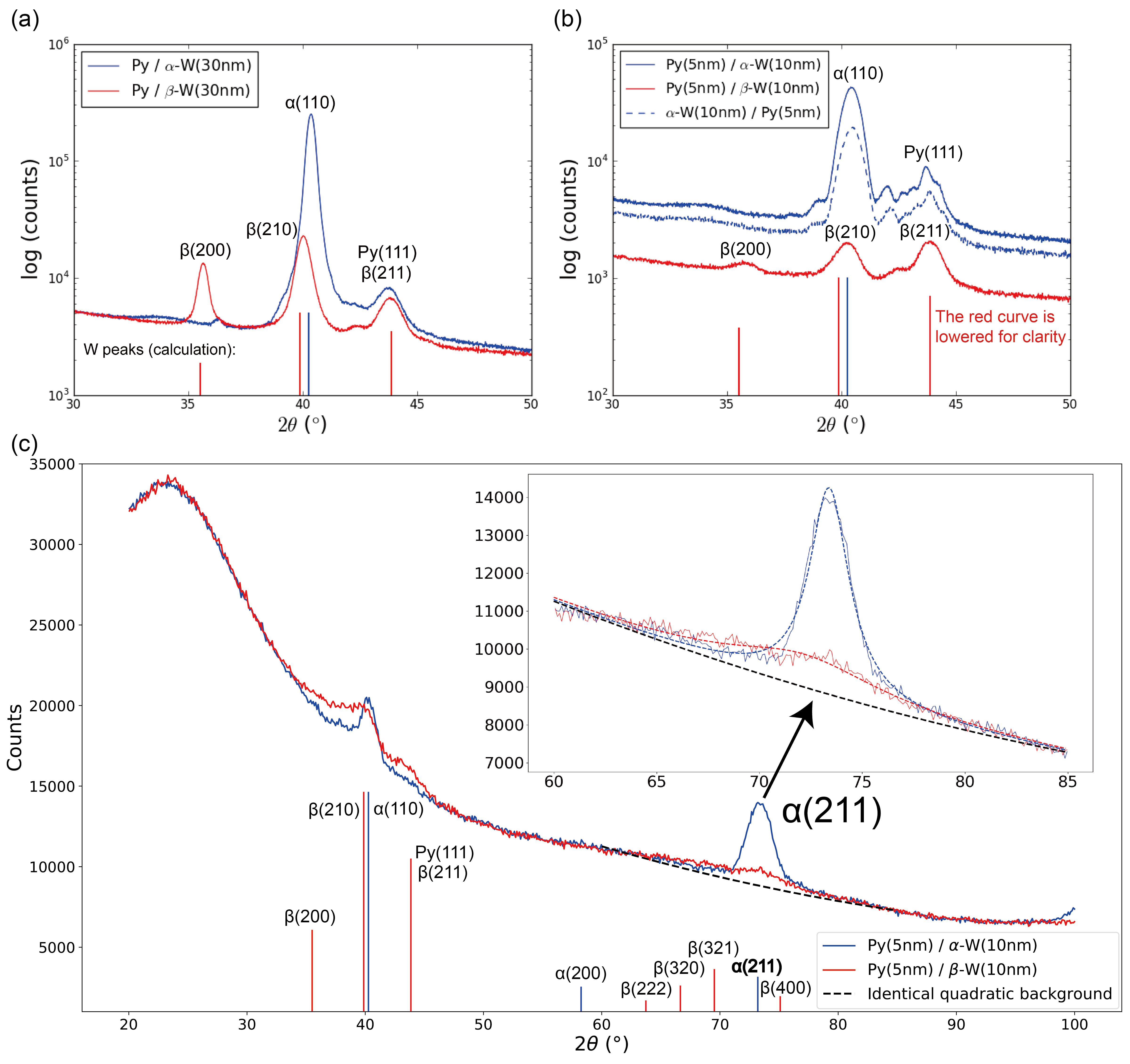
The symmetric (-) scans, with scattering vector perpendicular to film planes, are presented first. We point out some obvious features of the symmetric XRD spectra, shown in Figures 1a) and 1b). For the Py/“”-W(30 nm) film in Fig. 1a), all peaks can be indexed to the close-packed planes, Cu(111)/Py(111) (fcc) and -W(110) (bcc). The small peak at can be indexed to the reflection of a small amount of Cu radiation from -W(110). Moving to the thinner phase film in Fig. 1b), Py/“”-W(10 nm), it is still the case that all reflections can be indexed to the close-packed Cu(111)/Py(111) and -W(110) planes. However, there is greater structure in these reflections, presumably due to finite-size oscillations (Laue satellites), expected to be more evident in thinner films. Nearly identical spectra are recorded for the 10 nm “”-W films regardless of deposition order: Py(5 nm)/“”-W(10 nm) and “”-W(10 nm)/Py(5 nm) films scatter X-rays very similarly, as shown in Fig. 1b). We should note that Cu deposited on Ta has strong {111} texture in our films. Py (Ni81Fe19) deposited on Cu also has strong {111} texture; growth of Py on Cu and vice-versa is found to be largely coherent within grains. Both layers are fcc with similar lattice parameters: Å for CuBarmak and Liu (2017); Otte (1961) and Å for PyBarmak and Liu (2017); Huang et al. (1997), with a small misfit strain of . The XRD peaks for (111)-reflections in bulk phases, broadened by finite-size effects ( for 5 nm films, using the Scherrer equationScherrer (1918); Ying, Murray, and Noyan (2009)), are very close to each other, at (Py) and (Cu) respectively, so we expect (and have observed) one averaged peak for Cu and Py.
The nominal “”-W films (red lines) clearly show the presence of the phase through the unique -W(200) reflection at . This unique reflection is very strong in the “”-W(30 nm) heterostructure (Fig. 1a) but weaker as a proportion of the total intensity in the thinner “”-W(10 nm) heterostructure (Fig. 1b). In Fig. 1a), experimental -W(200) and -W(210) reflections have intensities in a ratio similar to the theoretical scattering intensity ratios for randomly-oriented grains. This is not the case for the thinner “”-W(10 nm) heterostructure in Fig. 1b); here the unique -W(200) peak is less intense than expected. We interpret the relative weakness of (200) as the presence of a large fraction of grains in the nominal Py/“”-W(10 nm) heterostructure.
In order to quantify the amount of -W in the nominal “”-W film, we have carried out grazing incidence measurements of Py(5 nm)/W(10 nm) samples () on the same diffractometer, as illustrated in Fig. 1c). The samples were measured at a fixed source position of with step size, fixed slit and the 15 mm beam mask. From the TEM measurements in Fig. 2b), we find that the deposited “”-W films have {110} texture, i.e., the hexagonal arrangement ( angles) of the {011} -W reflections away from the surface normal. Thus with the grazing incidence geometry, in which the scattering vector does not remain perpendicular to the film plane, the relative intensities of the peaks will not match theoretical calculations (vertical lines) based on randomly-oriented, untextured films. For example, the -W(200) peak (blue, in ) almost vanishes in the XRD scan here, due to the {011}-W texture.
Here we focus on the -W(211) peaks near , observed in both Py/“”-W and Py/“”-W samples. As shown in the Fig. 1c) inset, the -W(211) peaks (), were fitted as the sum of Lorentzian peak and identical background, assumed quadratic in , for both Py/“”-W and Py/“”-W samples. First we fit the -W(211) peak (blue) in the Py/“”-W sample to the summed function to determine the Lorentzian peak and quadratic background parameters. Next, we use this fitted background in the fit to the -W(211) peak (red) in the Py/“”-W sample. The two fitted -W(211) peaks are shown as blue (for Py/“”-W) and red (for Py/“”-W) dashed lines in the Fig. 1c) inset. The fits reproduce the experimental data well in the fitted region. The integrated -W(211) peak (i.e., the -integrated area between the measured data and the fitted background) for the Py/“”-W sample has roughly half the intensity of the integrated peak for the Py/“”-W sample. Assuming that the nominal -W is 100% phase and that the grains in mixed phase “”-W have similar {110} texture, as is supported by the HR-XTEM measurements in Figures 2 and 3, we conclude that the Py/“”-W(10 nm) film is roughly 50% -W and 50% -W.
III.2 Transmission electron microscopy
The phases of the nominal Py(5 nm)/“”-W(30 nm) and the nominal Py(5 nm)/“”-W(30 nm) samples deposited on oxidized Si substrates were characterized in high-resolution cross-sectional imaging, selected-area diffraction, and focused-beam nanodiffraction, by transmission electron microscopy (for details see the endnote11endnote: 1Focused ion-beam (FIB) and FEI Helios NanoLab 660 were used to prepare foils for TEM studies. To protect the heterostructures against the ion-beam damage during sample preparation, amorphous Platinum (1.5 thick) was sputtered on the surface of the wafers by electron and ion beam, respectively. TEM and high-resolution cross-sectional TEM (HR-XTEM) analyses were performed by image Cs-corrected FEI Titan Themis 200 at an accelerating voltage of 200 kV. Nano-beam electron diffraction pattern (DP) technique and Fourier transform (FT) analysis of the HRTEM have been utilized to identify the nature of each phase at the scale of 1–2 nm wide. The nano-beam DPs were obtained by FEI Talos TEM operating at 200 kV. The second condenser aperture was set to 50 to obtain a small beam-convergence angle. In the diffraction mode, the beam was condensed to a spot ( 1–2 nm) and a convergent electron beam diffraction (in this case, known as Kossel-Möllenstedt pattern) was acquired at different locations on the sample.).
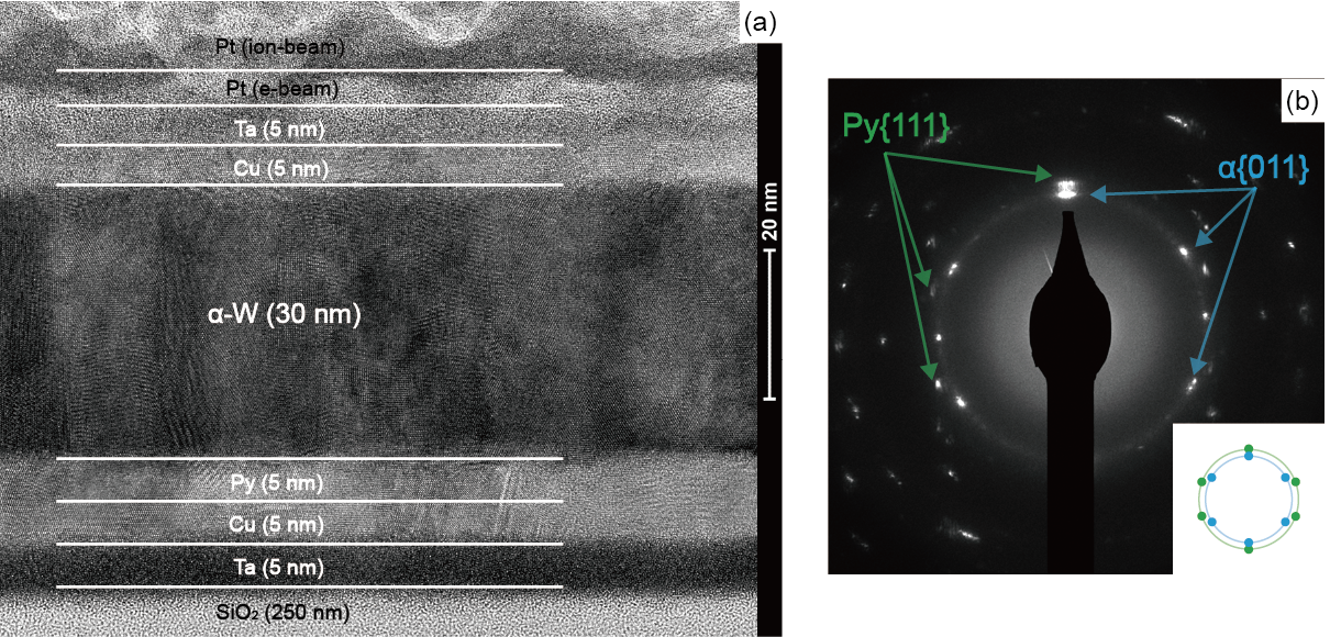
Fig. 2 shows a cross-sectional image and diffraction pattern for the nominal Py/“”-W(30 nm) heterostructure. First, one can see from the mass contrast between W and the 3d transition metal elements (Ni, Fe, Cu) that the Py/W and W/Cu interfaces are relatively flat and sharp on the scale of the image resolution of nm, presumably broadened by topographic variation through the thickness of the TEM foil. Second, based on (less pronounced) diffraction contrast parallel to the interface, the grains appear to be columnar, in many cases extending through the film thickness, with an average (lateral) grain diameter of 10–20 nm. The selected-area diffraction (SAD) pattern can be indexed according to unique (111)Py//(011)-W fiber texture, as shown by the hexagonal arrangement ( angles) of the {011} reflections in -W, and the arrangement of {111} reflections in Py, away from the (vertical) fiber axis. The calculated diffraction spots based on {111}Py//{011}-W fiber texture with -fold rotational symmetry about the film-normal axis are shown in Fig. 2 b), inset; good agreement is found.
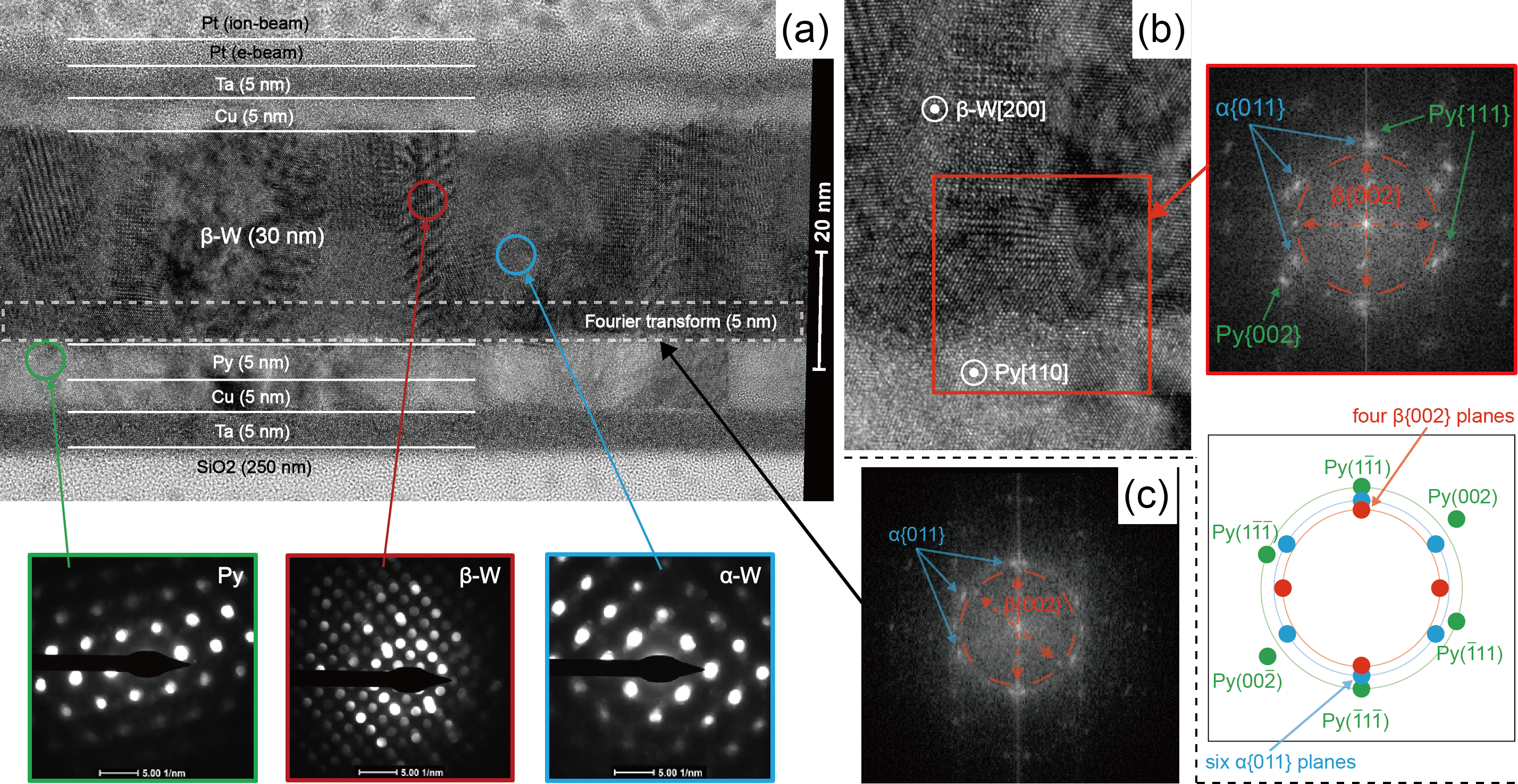
Cross-sectional images and diffraction patterns for the Py/“”-W(30 nm) heterostructure are shown in Fig. 3. Here again, in Fig. 3 a), the mass contrast shows similarly well-defined interfaces, but the topographic variations have a shorter wavelength, due presumably to smaller, more equiaxed grains in the mixed-phase “”-W. Circles indicate areas where convergent nanobeam electron diffraction (CBED) patterns were taken. The diffraction patterns over these small regions can be indexed to single phases: fcc Ni81Fe19 (Py) in green, bcc -W in blue, and A15 -W in red.
The CBED patterns in Fig. 3 a) confirm that the nominal “”-W film is mixed-phase -W and -W. The critical question for distinguishing the spin mixing conductances of -W and -W in Py/W is the identity of the W phase located within the first several nanometers of the interface with Py: the pumped spin current is ejected through the interface and absorbed over this region; see the x-axis of Fig. 6. We have addressed this question locally using high resolution imaging (see Fig. 3 b) and over a larger area using frequency analysis (see Fig. 3 c) of the image, roughly equivalent to SAD. In Fig. 3 b), a 10 nm area (red box) shows what appears to be a single-crystal region with ()[110]Py//(011)[]-W//(002)[200]-W, indicating that the crystals may nucleate on top of the crystals; however, this is contrary to our previous observationsBarmak and Liu (2017) and not distinguishable in the image from the superposition of grains through the foil, with nucleation of at the Py/W interface. The discrete spatial Fourier transform (FT) of this region shows that the four vertically/horizontally circled -W{002} spots are similar in intensity to the six -W{011} spots, supporting a similar -W content in this region. Carrying out a spatial FT of the full selected region within 5 nm of the interface (dotted box) in Fig. 3 a), we can confirm that -W is indeed present adjacent to the interface, as indicated by the -W{002} FT spots in Fig. 3 c), although these appear to be somewhat less intense than the -W{011} spots.
III.3 Resistivity
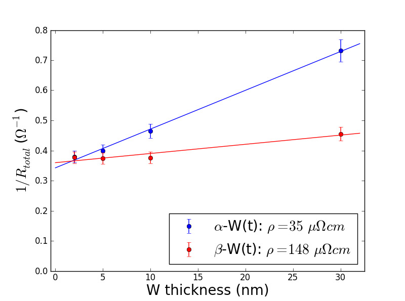
Four-point probe van der Pauw resistivity measurements were performed at room temperature on the first thickness series of samples ( fixed, variable ) deposited on mm square glass substrates, i.e., glass substrate/Ta(5 nm)/Cu(5 nm)/Py(5 nm)/W()/Cu(5 nm)/Ta(5 nm). Two point probes for current and two point probes for voltage were placed at the four corners of the square coupons. For square samples, the voltage-to-current ratios were converted to resistance per square using the known geometrical factor van der Pauw (1958). To isolate the W resistances, we plot the thickness-dependent sheet conductance and fit according to:
| (1) |
where () is the total resistance (conductance) of the sample, and are the resistivity and the thickness of the W layer, and is the parallel conductance of other layers in the stack.
We have verified Ohmic response by fitting the proportional dependence of voltage on current over the range 2 mA 10 mA for each sample. Fig. 4 summarizes the total conductance as a function of W thickness for all Py(5 nm)/W() heterostructures. Solid lines represent linear fits for the W resistivity , assumed constant as a function of W thickness for “”-W and “”-W samples. The extracted resistivity for “” phase W is found to be cm and for “” phase W cm. The resistivity for “”-W more than four times greater than that for “”-W, is due in large part to the much smaller grain size for -W and is typically observed in prior studiesPetroff et al. (1973). Here the resistivity for “-W” is larger by a factor of 2–3 than films deposited at room temperature and postannealed in previous workChoi et al. (2011), also attributable to a smaller grain size in these films deposited at ambient temperature. The resistivity measurements for these thin films might be taken as indirect evidence for the presence of the phase in the nominal “”-W layers.
IV ferromagnetic resonance measurements
The four thickness series of Py()/W() films, for “”-W and “”-W, as described in Section II were characterized using variable-frequency field-swept FMR using a coplanar waveguide (CPW) with center conductor width of 300 m. The bias magnetic field was applied in the film plane (pc-FMR, or parallel condition). For details, see e.g., our prior work in Ref. [20].
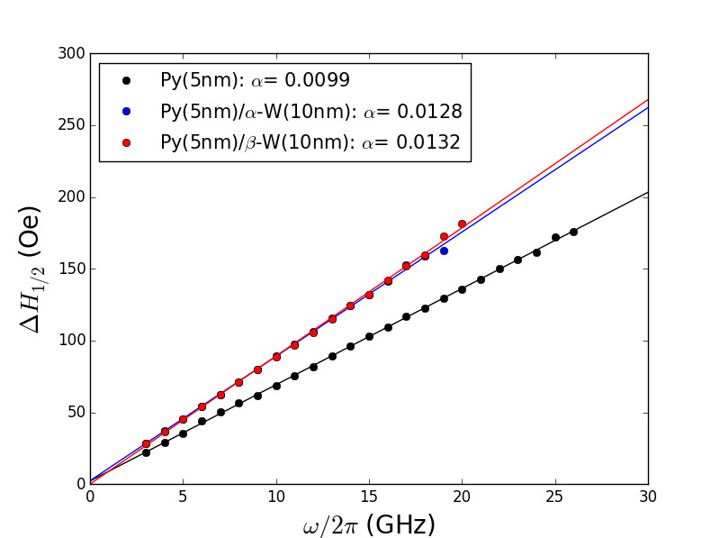
Fig. 5 summarizes half-power FMR linewidth as a function of frequency for Py(5 nm), Py(5 nm)/“”-W(10 nm) and Py(5 nm)/“”-W(10 nm) samples. The measurements were taken at frequencies from 3 GHz to above 20 GHz. Solid lines are linear regression of the variable-frequency FMR linewidth , where is the full-width at half-maximum, is the inhomogeneous broadening, is the Gilbert damping, is the resonance frequency and is the gyromagnetic ratio. Good linear fits were obtained with resonance frequency for experimental linewidths of all the samples measured.
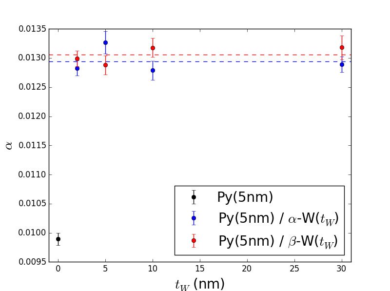
For the first sample thickness series Py(5 nm)/W(), we plot damping parameters extracted from the linear fits, as a function of W thickness in Fig. 6. Standard deviation errors in the fit for are . The Gilbert damping saturates quickly as a function of for both “”-W and “”-W, with almost all of the effect realized with the first 2 nm of W. Loosely speaking, this fast saturation implies a short spin diffusion length nm, so the identity of the W phase ( or ) over this length scale near the interface is most relevant. The averaged damping, and , are shown as horizontal dashed lines in the figure. is slightly smaller than , but this may be within experimental error. Due to spin pumping, the damping is enhanced with the addition of W layers , normalized to the Gilbert damping of the reference sample without W layers. The effective SMC at the Py/W interfaces can be calculated following:
| (2) |
where is the gyromagnetic ratio, is the reduced Planck constant, and kG is the saturation inductance of Py. In this series of samples, the effective SMC at the Py/“”-W interface nm-2 and the effective SMC at the Py/“”-W interface nm-2. These values are significantly lower than those reported in Ref.Demasius et al. (2016) for CoFeB/W (20–30 nm-2), as measured by spin-torque FMR.
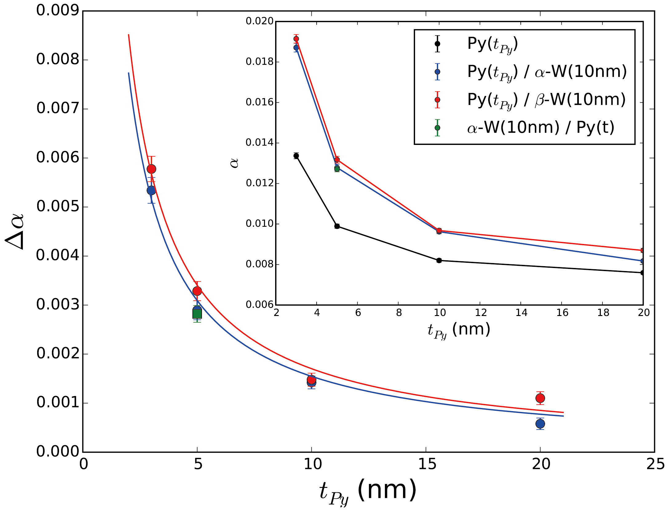
For the second sample thickness series Py()/W(10 nm), we plot the extracted Gilbert damping and damping enhancement as a function of Py thickness in Fig. 7. The enhanced damping is normalized to the Gilbert damping of reference samples with the same Py thickness . The result is in good agreement with the inverse thickness dependence of contributed damping predicted from Equation 2. The experimental data is fitted with Equation 2 to extract the effective SMC. In this series of samples, the effective SMC at the Py/“”-W interface nm-2 and the effective SMC at the Py/“”-W interface nm-2.
Previous studies on W have shown that the formation of -W is preferred, for thicker W layers (e.g. 10 nm)Choi et al. (2011); Pai et al. (2012). We also prepared the sample “”-W(10 nm)/Py(5 nm) with reverse deposition order, with the same seed and cap layers, on an oxidized Si substrate. Here the top surface of the 10 nm thick -W layer is pure phase, as shown by XRD in Fig. 1 a). We performed the same FMR measurement on the reverse order sample; its Gilbert damping enhancement is plotted as the green dot in Fig. 7. This point almost overlaps with the measurement for the normal order sample Py(5 nm)/“”-W(10 nm), indirectly supporting the conclusion that the phase of the Py/“”-W interface is similar to the phase of the “”-W/Py interface, i.e., almost 100% phase W. Note that it was not possible to deposit a reverse-order phase sample because no phase W could be stabilized on Cu using our techniqueBarmak and Liu (2017).
The FMR measurements of spin mixing conductance for Py/“”-W and Py/“”-W are new in this study. We find that the value is similar to that measured for TaMizukami, Ando, and Miyazaki (2001) ( 10 nm-2) regardless of the enriched phase. First-principles-based calculations including relativistic effectsLiu et al. (2014) for at Py/NM interfaces have shown that Ta, next to W in the periodic table, is a good spin sink due to its large spin-orbit coupling (SOC), but has a relatively small 8–9 nm-2. The efficient absorption of spin current can be connected with a large SOC from the large atomic number, and the low SMC can be connected to relatively poor band matching across the Py/W interface, compared with that for Py/Cu or Py/PtLiu et al. (2014). The conclusion for Ta is consistent with our experimental results for the Py/W system, i.e., the rapid saturation of Gilbert damping within the first 2 nm of W, indicating W is also a good spin sink, with a similarly low 7 nm-2.
V discussion
We have found very little difference between the spin scattering properties (spin mixing conductance and spin diffusion length) of -W and mixed phase (+)-W. The simplest interpretation is that both spin mixing conductances and spin diffusion lengths are nearly equal for the two phases. However, despite our development of an optimized techniqueLiu and Barmak (2016); Barmak and Liu (2017); Barmak et al. (2017) to stabilize the phase, our control over the amounts of deposited and phases is less than complete, particularly near the Py/W interface.
The “”-structure we deposited, Py/-W, is nearly 100% phase. We observed no strong -W peaks in the XRD scans, and neither crystalline structure nor diffraction patterns for the phase in HR-XTEM characterization. According to our previous workChoi et al. (2011, 2014); Barmak and Liu (2017), we know that ionically and covalently bonded substrates/underlayers are favorable for the formation of some -W, whereas metallic underlayers promote , so on Py even at a thickness of 2 nm, the nominally -W film is fully if deposited in the absence of nitrogen.
In the thinnest “”-structure which we can characterize by XRD, Py/“”-W(10 nm), we identify a roughly 50%-50% mixture of and phases. If this balance persists at the interface as well, the SMC cannot differ by more than 10-20% for the two phases. While the measurement of the 5 nm region near the interface seems to show somewhat less than 50% phase, there is still a substantial population of -W in this region, and it would seem that a strong difference in SMC for -W and -W should be resolvable if present. Given that the measured values are very similar, we conclude that the and phases do not differ strongly in this spin transport study.
One might ask why the spin mixing conductance, in contrast to the spin Hall anglePai et al. (2012), does not differ much for the two phases of W. The spin mixing conductance (SMC) is a property of the FM/NM interface, rather than a bulk property of the NM layer. The SMC may be approximated (in a single-band, free-electron model) as , where is the Fermi wave number for the NM, represents the number of scattering channels in units of one channel per interface atom, and A is the total surface area of the interfaceTserkovnyak, Brataas, and Bauer (2002b). Despite the possibility that bulk -W has a stronger effective spin-orbit coupling and spin Hall effect due to its A15 structure, -W could have similar numbers of conducting channels per atom at the FM/NM interface as -W, which could lead to the similar values of SMC measured here.
Another possibility is that the spin diffusion length may vary along the W layer thickness, due to nonuniformly distributed -W and -W phases in “”-W samples. If this is true, fitting a single spin diffusion length for spin pumping into very thin W layers will be problematicMontoya et al. (2016). However, because we have observed a very rapid saturation of Gilbert damping over the first 2 nm of W for both “”-W (almost pure phase) and “”-W (mixed phase) in Fig. 6, we can only assign an upper bound for , similarly short in the two phases.
VI conclusions
In summary, we report measurements of spin mixing conductances of Py/W films with controlled amounts of and phase W, measured by Gilbert damping through ferromagnetic resonance (FMR). We find no strong differences in the spin mixing conductances of Py/-W and Py/-W, measured as 6.7–7.4 nm-2, although control of the phase is seen to be more difficult near the interface with Py. Our experimental results also indicate that W, no matter of which phase, is a good spin sink, but with relatively small spin mixing conductance in Ni81Fe19 (Py)/W, similar to Ta in Py/Ta.
VII acknowledgements
The authors thank Daniel Paley of Columbia Nano Initiative for the grazing incidence XRD scans and Kadir Sentosun of Columbia University for the satellite peak calculations. This work is supported by the US NSF-DMR-1411160.
References
- Saitoh et al. (2006) E. Saitoh, M. Ueda, H. Miyajima, and G. Tatara, Applied Physics Letters 88, 182509 (2006).
- Liu et al. (2011) L. Liu, T. Moriyama, D. C. Ralph, and R. A. Buhrman, Phys. Rev. Lett. 106, 036601 (2011).
- Pai et al. (2012) C.-F. Pai, L. Liu, Y. Li, H. W. Tseng, D. C. Ralph, and R. A. Buhrman, Applied Physics Letters 101, 122404 (2012).
- Wang et al. (2014) H. L. Wang, C. H. Du, Y. Pu, R. Adur, P. C. Hammel, and F. Y. Yang, Phys. Rev. Lett. 112, 197201 (2014).
- Hartmann, Ebert, and Bretschneider (1931) H. Hartmann, F. Ebert, and O. Bretschneider, Z. Anorg. Allg. Chem. 198, 116 (1931).
- Hao and Xiao (2015) Q. Hao and G. Xiao, Phys. Rev. Applied 3, 034009 (2015).
- Liu et al. (2015) J. Liu, T. Ohkubo, S. Mitani, K. Hono, and M. Hayashi, Applied Physics Letters 107, 232408 (2015).
- Demasius et al. (2016) K.-U. Demasius, T. Phung, W. Zhang, B. P. Hughes, S.-H. Yang, A. Kellock, W. Han, A. Pushp, and S. S. P. Parkin, Nature Communications 7, 10644 (2016).
- Liu and Barmak (2016) J. Liu and K. Barmak, Acta Materialia 104, 223 (2016).
- Barmak and Liu (2017) K. Barmak and J. Liu, Journal of Vacuum Science & Technology A: Vacuum, Surfaces, and Films 35, 061516 (2017).
- Barmak et al. (2017) K. Barmak, J. Liu, L. Harlan, P. Xiao, J. Duncan, and G. Henkelman, The Journal of Chemical Physics 147, 152709 (2017).
- Arita and Nishida (1993) M. Arita and I. Nishida, Japanese Journal of Applied Physics 32, 1759 (1993).
- Hägg and Schönberg (1954) G. Hägg and N. Schönberg, Acta Crystallographica 7, 351 (1954).
- Urban, Woltersdorf, and Heinrich (2001) R. Urban, G. Woltersdorf, and B. Heinrich, Phys. Rev. Lett. 87, 217204 (2001).
- Tserkovnyak, Brataas, and Bauer (2002a) Y. Tserkovnyak, A. Brataas, and G. E. W. Bauer, Phys. Rev. Lett. 88, 117601 (2002a).
- Mosendz et al. (2010) O. Mosendz, J. E. Pearson, F. Y. Fradin, G. E. W. Bauer, S. D. Bader, and A. Hoffmann, Phys. Rev. Lett. 104, 046601 (2010).
- Caminale et al. (2016) M. Caminale, A. Ghosh, S. Auffret, U. Ebels, K. Ollefs, F. Wilhelm, A. Rogalev, and W. E. Bailey, Phys. Rev. B 94, 014414 (2016).
- Li, Cao, and Bailey (2016) Y. Li, W. Cao, and W. E. Bailey, Phys. Rev. B 94, 174439 (2016).
- Cao et al. (2019) W. Cao, L. Yang, S. Auffret, and W. E. Bailey, Phys. Rev. B 99, 094406 (2019).
- Otte (1961) H. M. Otte, Journal of Applied Physics 32, 1536 (1961).
- Huang et al. (1997) J. Huang, T. Wang, C. Yu, Y. Hu, P. Lee, and M. Yang, Journal of Crystal Growth 171, 442 (1997).
- Scherrer (1918) P. Scherrer, Göttinger Nachrichten Math. Phys. 2, 98 (1918).
- Ying, Murray, and Noyan (2009) A. J. Ying, C. E. Murray, and I. C. Noyan, Journal of Applied Crystallography 42, 401 (2009).
- van der Pauw (1958) L. J. van der Pauw, Philips Tech. Rev. 20, 220 (1958).
- Petroff et al. (1973) P. Petroff, T. T. Sheng, A. K. Sinha, G. A. Rozgonyi, and F. B. Alexander, Journal of Applied Physics 44, 2545 (1973).
- Choi et al. (2011) D. Choi, B. Wang, S. Chung, X. Liu, A. Darbal, A. Wise, N. T. Nuhfer, K. Barmak, A. P. Warren, K. R. Coffey, and M. F. Toney, Journal of Vacuum Science & Technology A: Vacuum, Surfaces, and Films 29, 051512 (2011).
- Mizukami, Ando, and Miyazaki (2001) S. Mizukami, Y. Ando, and T. Miyazaki, Journal of Magnetism and Magnetic Materials 226-230, 1640 (2001), proceedings of the International Conference on Magnetism (ICM 2000).
- Liu et al. (2014) Y. Liu, Z. Yuan, R. J. H. Wesselink, A. A. Starikov, and P. J. Kelly, Phys. Rev. Lett. 113, 207202 (2014).
- Choi et al. (2014) D. Choi, X. Liu, P. K. Schelling, K. R. Coffey, and K. Barmak, Journal of Applied Physics 115, 104308 (2014).
- Tserkovnyak, Brataas, and Bauer (2002b) Y. Tserkovnyak, A. Brataas, and G. E. W. Bauer, Phys. Rev. Lett. 88, 117601 (2002b).
- Montoya et al. (2016) E. Montoya, P. Omelchenko, C. Coutts, N. R. Lee-Hone, R. Hübner, D. Broun, B. Heinrich, and E. Girt, Phys. Rev. B 94, 054416 (2016).