Even-odd dependent optical transitions of zigzag monolayer black phosphorus nanoribbons
Abstract
We analytically study the electronic structures and optical properties of zigzag-edged black phosphorene nanoribbons (ZPNRs) utilizing the tight-binding (TB) Hamiltonian and Kubo formula. By solving the discrete Schordinger equation directly, we obtain the energy spectra and wavefunctions for a -ZPNR with number of transverse zigzag atomic chains, and classify the eigenstates according to the lattice symmetry. We then obtain the optical transition selection rule of ZPNRs based on the symmetry analysis and the analytical expressions of the optical transition matrix elements. Under an incident light linearly-polarized along the ribbon, importantly, we find that the optical transition selection rule for the -ZPNR with even- or odd- is qualitatively different. In specification, for even- ZPNRs the inter- (intra-) band selection rule is odd (even), since the parity of the wavefunction corresponding to the th subband in the conduction (valence) band is due to the presence of the symmetry. In contrast, all optical transitions are possible among all subbands due to the absence of the symmetry. Our findings provide a further understanding on the electronic states and optical properties of ZPNRs, which are useful in the explanation of the optical experiment data on ZPNR samples.
pacs:
71.45.-d, 71.10.+x, 71.70.-d, 75.10.-bI Introduction
Black phosphorus (BP) is a layered material similar to graphite with the atomic layers coupled by van der Waals interactions YBZhang ; Ye ; StevenP ; FengnianXia . Few-layer YBZhang ; Ye ; StevenP ; FengnianXia ; Buscema and monolayer Ye ; Andres ; Lu ; xmwang BP (termed as phosphorene) have been fabricated experimentally, attracted intensive attentions due to their unique electronic properties and potential applications in nanoelectronics Xiling ; Gomez ; YBZhangPL . Unlike graphene, BP is a semiconductor possessing a direct band gap ranging from 0.3 eV to 1.8 eV depending on the thicknesses of BP samples xmwang ; YBZhangPL . The field-effect-transistor (FET) based on phosphorene is found to have an on/off ratio of 103 and a carrier mobility of 800 cm2/Vs Sherman . Sizable band gap and relatively high mobility in phosphorene bridge the gap between graphene and transition metal dichalcogenides (TMDs), which are important for electronics and optoelectronics Xiling ; Gomez ; YBZhangPL . Inside phosphorene, phosphorus atoms are covalently bonded with three adjacent atoms to form a puckered honeycomb structure due to the hybridization Rodin . Arising from the low symmetric and high anisotropic structure, BP exhibits strongly anisotropic electrical Ye ; xyzhou ; xyzhouoptic ; rzhang ; xyzhougfactor , optical Tony2 ; Tran ; YBZhangPL ; xmwang and transport Zhenhua properties.
The band structure of 2D phosphorene can be well described by a four band tight-binding (TB) model Rudenko ; Rudenkogap . Tailoring it into 1D nanoribbons offer us a way to tune its electronic and optical properties due to the quantum confinement and unique edge effects Tran ; Carvalhopnr ; hanxy ; ezawa ; Taghizadeh ; Zahra . The band structure of phosphorene nanoribbons (PNRs) depends on the edge configurations Tran ; Carvalhopnr ; hanxy ; ezawa ; Taghizadeh ; Zahra . The armchair-edged PNRs (APNRs) are semiconductors with direct band gap sensitively depending on the ribbon width with scaling law of Tran ; Taghizadeh ; Zahra , while the bare zigzag-edged PNRs (ZPNRs) are metallic regardless of their ribbon width due to the quasi-flat edge states Carvalhopnr ; ezawa . In bare ZPNRs, the edge states are entirely detached from the bulk bands and localized at the boundaries. These edge states result in a relatively large density of states near the Fermi energy ezawa ; Longlong Zhang . Further, the band structure of ZPNRs can be effectively modified by tensile strain hanxy or electric field hanxy ; ezawa ; HGuo . Very recently, few-layer ZPNRs are successfully synthesized in recent experiments Paulmd ; NakanishiAyumi . Up to date, various interesting properties have been predicted for ZPNRs, including those related to transverse electric field controlled FET ezawa , room temperature magnetism and half metal phase wucj ; yujia ; Reny , strain induced topological phase transition Sisakhtet , and symmetry dependent response to perpendicular electric fields Zhoubl , etc.
On the other hand, although there are already many research works on 2D phosphorene and its 1D ribbons, the analytical calculation on the band structure of ZPNR is still lacking. Most of the previous works on this issue are based on the first-principles calculation Tran ; Carvalhopnr ; hanxy ; HGuo or numerical diagonalization utilizing the TB model ezawa ; Taghizadeh . As well, there is also less attention has been paid to the optical property of ZPNR Zahra ; Sima , and particularly the optical transition selection rule in relation to the lattice symmetry and wavefunction parity are not fully understood. Optical spectrum measurements are fundamental approach to detect and understand the crystal band structure, which have been successfully performed for 2D phosphorene YBZhangPL . To this end, in this work we theoretically investigate the optical properties of ZPNRs based on the TB model and the Kubo formula. By solving the discrete Schordinger equation analytically, we obtain the electronic structures of ZPNRs and classify their eigenstates according to the crystal symmetry. We then obtain the optical transition selection rules of ZPNRs directly based on the symmetry analysis and the analytical expressions of the optical transition matrix elements. When the incident light is polarized along the ribbons (see Fig. 1), interestingly, we find that the optical selection rules change significantly for a -ZPNR with even- or odd-. In particular, for even- ZPNRs the electronic wavefunction parity of the th subband in the conduction (valence) band is due to the symmetry, and therefore their inter- (intra-) band selection rule is ==odd (even). For odd- ZPNRs without symmetry, in contrast, the optical transitions are all possible among subbands. Further, the edge states of both even- and odd- ZPNRs play an important role in the optical absorption. Moreover, impurities or external electric field can break the symmetry of even- ZPNRs, which consequently enhances the optical absorption.
The paper is organized as follows. Sec. II mainly presents the analytical result. We first repeat the numerical diagonalization procedure to obtain the band structure for the system, and the detailed analytical calculations on the band structure with particularity of approaching accurate edge bands are followed. Then the wavefunctions, the joint density of states and the optical conductivity for ZPNRs are expressed. In Sec. III, we present some numerical examples and discussions on the band structure and optical absorptions of the ZPNRs. Finally, we summarize our results in Sec. IV.
II Electronic structure and optical properties
II.1 Numerical diagonalization on Hamiltonian
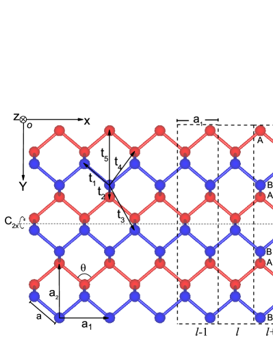
The puckered honeycomb structure of phosphorene is shown in Fig. 1, where the red and blue dots represent phosphorous atoms in different sub-layers. There are four atoms in one unit cell with the primitive vectors Å and Å. The bond length between two adjacent atoms is =2.207 Å with bond angle =96.79∘ Rudenko . Tailoring phosphorene into 1D nanoribbons along the zigzag direction leading to ZPNRs. The length of the bond connecting different sub-layers is 2.207 and the layer spacing is Å. The integers 1, 2, describe the number of the zigzag atomic chains of a ZPNR along its transversal direction. In the TB framework Rudenko ; Rudenkogap , the Hamiltonian of a phosphorene in the presence of in-plane transverse and of-plane vertical electric fields as well as impurities can be generically written as
| (1) |
where the summation runs over all neighboring atomic sites with hopping integrals , and () is the creation (annihilation) operator for atom site (). It has been shown that five hopping parameters (see Fig. 1) are enough to describe the electronic band structure of phosphorene Rudenko with hopping energies =1.22 eV, =3.665 eV, =0.205 eV, =0.105 eV, and =0.055 eV. A uniform vertical electric field will result in a staggered potential between the upper (=1) and lower () sublayers due to the puckered structure Zhoubl ; R.Ma . Applying a transverse electric field will shift the on-site energy to with the atom coordination in the -direction, and is the impurity potential.
For a -ZPNR with the number of zigzag chains across the width, by applying the Bloch’s theorem the TB Hamiltonian in the momentum space is Datta
| (2) |
where Hamiltonian () describes the intra (inter)- supercell [see the (black) dashed-line rectangles in Fig. 1] interactions, is the wavevector along the -direction. In our calculation, we accordingly choose the basis ordered as ( to write done and in the form of () matrix for the super cell adopted. Then, we can obtain the energy spectrum and the corresponding wavefunction for the system by numerical diagonalization. In real space, the wavefucntion can be formly expressed as
| (3) |
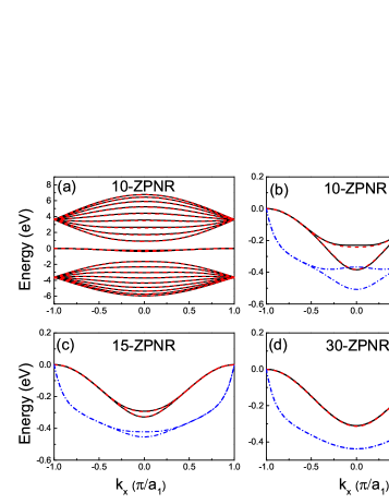
where = is the electron coordination, = is the atomic position vector, = is the eigenvector of the Hamiltonian matrix in Eq. (2) with the transpose operator , and is a Guass broadening parameter. Up to now, the band structure of ZPNRs is well understood by the first-principles calculations Tran ; Carvalhopnr ; hanxy ; HGuo or numerical TB calculations ezawa ; Taghizadeh . For comparison here, the band structure of our numerical diagonalization for a 10-ZPNR is shown by the (black) solid lines in Fig. 2(a), which is in good agreement with the existed results ezawa ; Taghizadeh . We note that there is a little difference compared with that of the first-principles calculation Tran ; Carvalhopnr ; hanxy ; HGuo due to the relaxation of the edge atoms. Considering the limitation of the first-principles calculation, the TB model can be applied to study the ZPNRs with large widths. More importantly, we give the analytical solutions for electronic states and optical transitions in the ZPNRs with arbitrary widths. In comparison with the previous numerical calculations Tran ; ezawa ; Taghizadeh ; Carvalhopnr ; hanxy ; HGuo , the analytical results are more convenient to do further understand in the electronic property of ZPNRs, i.e., identifying the subband symmetry property and calculating the optical absorption. Hereafter, we will present the analytical calculations on the band structure of ZPNRs in the next subsection.
II.2 Analytical calculation on electronic structure
In this subsection, we firstly outline a scheme to obtain the analytical energy spectrum for ZPNRs by solving the TB model directly. According to the TB approximation, the discrete Schordinger equation for a -ZPNR is
| (4) | ||||
where =, is the wavefuntion of the th A/B atom, and the site index . Since the B and A sites are missing, we naturally have the hard-wall boundary condition for ZPNRs as
| (5) |
According to the Bloch theorem, the generic solutions for and can be written as
| (6) |
where , , and are arbitrary coefficients and the wavenumber in the transverse direction, which can be defined by the Schordinger equation combined with the boundary condition. Substituting Eq. (6) into (5), the wavefunction can be simplified as
| (7) | ||||
where . Meanwhile, substituting Eq. (7) into (4), we obtain a matrix equation
| (8) |
where M is a 22 matrix with elements
The condition for nontrivial solutions of and in Eq. (8), namely , is det()=0. However, it is worth to note that the solutions of and should be excluded as unphysical results because these values of yield =0 [see Eq. (7)] for arbitrary . In other words, electrons are absent in the system in these cases, which is unphysical. Therefore, we should find solutions that satisfy det()=0 for arbitrary except , . After some arithmetic, we find that the equation det()=0 yields the following equation
| (9) |
where , and are functions of , and . Generally, Eq. (9) should be valid for arbitrary . Thus, the two coefficients ( and ) of and the constant term should be zero. We then obtain the energy spectrum for ZPNR as
| (10) |
where represent the conduction and valence bands, respectively.
On the other hand, from =0, we find a transcendental equation for the transverse wavevector which can be determined by
| (11) | ||||
This equation implies that the transverse wavenumber depends not only on the ribbon width but also on the longitudinal wavenumber . Obviously, we have , which means that Eq. (11) defines the same subbands for and . Hence, we can simply find the solutions of from Eq. (11) in the later interval. If = and , Eq. (11) reduces to the transcendental equation for a zigzag-edged graphene nanoribbon (ZGNR) case Katsunori ; Saroka . Similar to that in a -ZGNR, there are only - nonequivalent solutions of Eq. (11) for , which defines - subbands, namely the bulk states of a ZPNR.
Notably, the two edge states are naturally missing in the scheme here since the transverse wavevector are purely imaginary as is described by Eq. (6). But fortunately we can restored them by setting and do the same procedure above to obtain the eigenenergy and the corresponding transcendental equation. In this case, the eigenenergy in Eq. (10) can be rewritten as
| (12) |
where , with the corresponding transcendental equation expressed by
| (13) | ||||
where is the hyperbolic sine function. Obviously, we have =, which means we only need to find the solution of for case.
Therefore, according to Eq. (10), we can obtain the band structure of ZPNRs by this analytical approach. We present an example of bulk band structure in Fig. 2(a), where the (red) dashed lines describe the analytical result for 10-ZPNR, which exactly matches our previous numerical one [see the (black) solid lines] starting from Eq. (2). In addition, the edge bands of different 10-, 15- and 30-ZPNR are also shown in Figs. 2(b-d), where the (black) solid and (blue) dash-dotted lines represent the numerical and analytical results, respectively. Unfortunately, we can see that the analytical results for edge states given by Eq. (12) are not in consistent with the numerical ones. This discrepancy was also revealed in a recent work M. Aminic . We think that the discrepancy mainly originates from the hopping links , and , with which their hopping distances are beyond a zigzag chain (see Fig. 1). This makes the discrete Schordinger equation (4) is invalid for the edge atoms, namely equal to 1 or . To resolve this problem, one solution is choosing four atoms to write down Eq. (4) and double the number of the boundary condition (5). But this method will enlarge the dimensions of matrix unavoidably and make the problem to be quite complicate and difficult to solve.
Hereby, we propose an efficient solution to eliminate this discrepancy by simply adding a correction term. Generally, the two edge states can be described by a 22 matrix Hamiltonian as
| (14) |
where describes the two degenerate edge states when the ribbon width is large, and describes the coupling between the edge states for small . Based on this argument, according to Eq. (12), we have and . The band structure of the edge states in 10-, 15- and 30-ZPNR given by Eq. (12) are presented by the (blue) dash-dotted lines in Figs. 2(b-d), respectively. From these figures, we find that is finite for a narrow ribbon as shown in Fig. 2(b) for 10-ZPNR, but it vanished for the wider ones [e.g., Fig. 2(d) for 30-ZPNR]. This means that is suitable to describe the coupling between the edge states. However, there is a observable discrepancy between the analytical results [Eq. (12)] shown by the (blue) dash-dotted lines and the numerical ones [the (black) solid lines] in Figs. 2(b-d). This implies that is unsuitable to describe the edge states and needs a correction so as to describe the edge bands accurately. Naturally, we can assume that the correction term is a superposition of the energy term caused by hopping links (, , ) beyond one zigzag chain, which is expressed as
| (15) |
where the coefficients , , , and . Then the energy of edge states can be written as
| (16) |
The analytical edge states expressed by Eq. (16) are also depicted by the (red) dashed lines in Figs. 2(b-d). Comparing them with the numerical data [the (black) solid lines], we find that they are in excellent agreement with each other regardless of the ribbon width, which indicates that our method is valid and reliable.
On the other hand, for the wavefunction (3), owing to the translational invariance along the -direction we can rewrite it in another generic form
| (19) |
where and are the normalization coefficient, the number of A and B atoms in a super-cell of a ZPNR, and the -coordination of the th atoms. Notably, Eq. (17) is the wavefunction for the bulk states of ZPNRs. For edge states, we should replace the transversal wavevector by .
As for the wavefunction of even- ZPNRs, we can obtain the relation = in Eq. (7) from the parity of a ZPNR, namely = Katsunori . The reason is that the wavefunction of even- ZPNRs is either symmetric or antisymmetric which is similar to that in ZGNRs Mahdi Moradinasab . Specifically, combined with the translational invariance along the -direction, the wavefuntion of even- ZPNRs is specified as
| (22) | |||||
| (25) |
where = is the normalization coefficient, indicates the parity of the subbands. Notably, Eq. (18) is the wavefunction for bulk states of even- ZPNRs. For edge states, the wavefunction (=) is
| (28) |
where = is also a normalization coefficient. On the contrary, owing to the absence of the symmetry, there is no such a simple expression of wavefunction for the odd- ZPNRs.
II.3 Optical property and transition selection rules
In order to detect the above calculated band structure of ZPNRs, we study its optical response in this subsection. One useful physical quantity to understand the optical property is the joint density of states (JDOS) representing all possible optical transitions among the subbands, which is generally given by
| (29) |
where the sum runs over all states and , is 2 for spin degree, the ribbon length, the photon energy, and the Fermi-Dirac distribution function with Boltzman constant and temperature . Here, we take a Guass broadening to approximate the -function, where is a phenomenological constant accounting for the energy level broadening factor. Meanwhile, assuming the incident light is polarized along the longitudinal (-) direction, the optical conductance based on the Kubo formula is given by Ando1 ; Ando2
| (30) |
where = is the velocity operator, which is valid and independent of the band structure model, and Burt is the total electron wavefunction in a ZPNR. Here is the envelop function which describes the slowly varying electron sharing movement in the crystal, while is the band edge wavefunction (BEW) connecting to the atom orbits directly describing the fast movement in the crystal. In a ZPNR, is composed by , , , and atomic-orbits with different weights Ruo-Yu Zhang ; WeifengLi . For a linear polarized light, the optical transition matrix elements satisfy =. Obviously, = determines the optical transition selection rules. A zero matrix element means a forbidden transition. The inner product between the two BEWs is subband dependent, with which only affects the amplitude of the optical conductance but does not change the optical selection rules. We take the inner production around the -point () as an approximation and treat it as a constant. This approximation has also been used in the previous work Tony2 for 2D phosphorene. We have omitted this constant in our calculations because the specific expression of the BEWs in ZPNRs are currently unknown. This approximation would not change the essential physics, i.e., the even-odd dependent optical selection rule, reported here. Note that in some topological none-trivial system, the dipole optical matrix result in the winding number Likunshi ; Tingcao . But there is no such an effect in phosphorene because it is a topologically trivial system. The real part of indicates the optical absorption when an laser beam incidents on the sample. Moreover, we can obtain the dielectric function from optical conductance by using =1+ Peteryu .
In optical transition process, selection rules determined by the matrix elements are the most important information. The integral of the velocity matrix elements = is proportional to the optical transition probability between the th and th subbands. Generally, the selection rule is always constrained by the symmetry of the system. Hence, in order to obtain a general optical selection rule for ZPNRs, we firstly check their lattice symmetry. According to Fig. 1, we find the lattice symmetry of a -ZPNR is even-odd- dependent. In particular, the even- ones have a operator with respect to the ribbon central axis (see the dotted horizontal line in Fig. 1). This is equivalent to the symmetry operator , where and are the mirror symmetry operators corresponding to the and the planes, respectively. However, the odd- ones do not have this symmetry. In even- ZPNRs, the constraint on the eigenstates imposed by symmetry is =. Assuming is the eigenvalue of operator, we have
| (31) |
Then we obtain =1, i.e., =1, where means the even/odd parity provided by the operator. This indicates that is either symmetric or antisymmetric along the and directions, namely =. Thus, we can classify the eigenstates for even- ZPNRs as even or odd parity according to the eigenvalues of the operator.
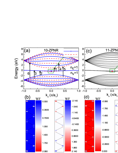
In order to confirm the above argument on the symmetry and parity for the systems, we present the band structure and the wavefunction in real space of the first subband in the conduction and valence bands for 10- and 11-ZPNR in Figs. 3(a-b) and 3(c-d), respectively. The wavefunction corresponding to states indicated by the red (blue) dots in Figs. 3(a) and 3(c) are shown in the left (right) panels in Figs. 3(b) and 3(d), respectively. According to the left (right) panel in Fig. 3(b), we find that the first subband in the conduction (valence) band is even (odd) under transformation. By checking the eigenstates in other subbands, we observe that the parity of wavefunctions varies alternatively from odd [(blue) solid lines] to even [(red) dashed lines] with the increase of subband index . This is consistent with the previous results obtained by the first-principles calculation Zahra ; Tran . Hence, the parity of the subband in the conduction (valence) band is related to its subband index via . Further, under the operation, the velocity operator is even, i.e., . Hence, we obtain the condition for none zero matrix element is that the parity of the initial () and final () states are the same. In other words, only the transitions among the states with identical parity are allowed. This can also be verified by calculating the optical transition matrix element. For example, using the relation combined with the wavefunction Eq. (18), the inter-band optical transition matrix element between the bulk states is Peteryu
| (32) |
is the wavefunction in Eq. (18) or (19). After some algebra, we have
| (33) |
where
Here and the detailed calculations on Eq. (24) are presented in the Appendix A.
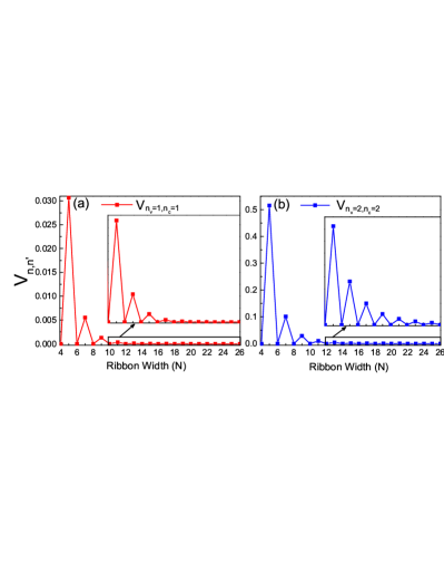
From Eq. (24), we can explicitly find that only the inter-band transition between the bulks states with the same symmetry are allowed. Using the wavefunction in Eq. (19), we can obtain the same selection rules for the transition between the edge bands as well as that between the bulk bands and edge bands. Hence, we conclude that only the transitions between the subbands with same parity are allowed. Consequently, in even- ZPNRs, the inter (intra)-band selection rule is ==odd (even). This is in good agreement with the above analysis based on the lattice symmetry. It is important that although the band structure of odd- ZPNRs is similar to that of even- ones as shown in Fig. 3(c), the optical selection rule is qualitatively different from that for even- ZPNRs. According to the left (right) panel in Fig. 3(d), by checking the eigenstates within the whole band, we know that there is no subband owning definite parity in 11-ZPNR due to the absence of symmetry. Thus, the optical transitions in odd- ZPNRs between two arbitrary subbands are all possible. In order to illustrate the even-odd dependent optical selection rule more clearly, in Fig. 4 we show the integral of the optical transition matrix elements as a function of the ribbon width , where (a) for and (b) for , respectively, and the insets show the amplified picture of on ribbon width with large . Physically, is proportional to the optical transition probability between the th and th subbands. According to the figure, we find that the transition probability oscillates with the ribbon width and shows an even-odd dependent feature. The transitions between the subband =1 (2) and =1 (2) are forbidden in even -ZPNRs due to the presence of the symmetry. In contrast, the transitions between the subband =1 (2) and =1 (2) are allowed in odd -ZPNRs due to the absence of the symmetry. This even-odd dependent selection rule is also reflected in the optical absorption spectrum which will be discussed in the nest section.
III Numerical Results and Discussions
In this section, we present some numerical examples for the optical absorption spectrum of ZPNRs and discuss the corresponding results. We take =10 and 11 to represent the even and odd cases, respectively, which would not qualitatively influence the results here. The temperature is 4 K and the level broadening is 4 meV throughout the calculation unless specificated. In all following figures, the green solid line (if available) indicates the Fermi level.
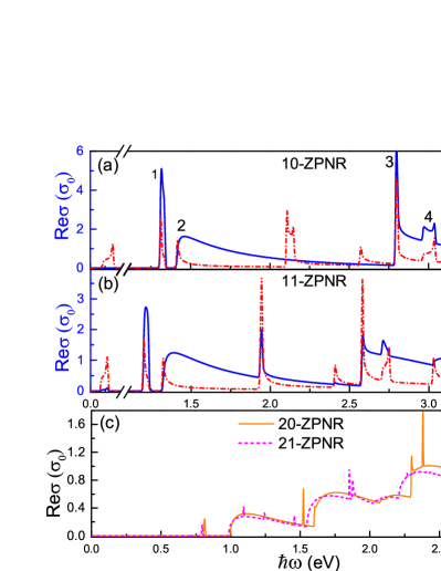
As discussed in Sec. IIC, the inter- (intra-) band optical transition selection rule in even- ZPNRs satisfies ==odd (even) due to the symmetry. On the contrary, the optical transitions in odd- ZPNRs between two arbitrary subbands are all possible resulting from the symmetry breaking. Keeping this in mind is important to understand the optical properties of even- ZPNRs. Fig. 5 shows the inter-band JDOS and the optical absorption spectrum for (a) 10-ZPNR and (b) 11-ZPNR with Fermi energy 0.3086 eV lying between the edge states, respectively. As shown by the (red) dash-dotted line in Fig. 5(a), we see peaks in the JDOS spectrum at different photon energy known as van Hove singularities. The JDOS peaks range from the mid-infrared (155-413 meV) to the visible region due to the edge states and the quantum confinement, which is different from that of 2D phosphorene case YBZhangPL . However, there is no optical absorption around zero frequency, which is contradict to the fact that ZPNRs are metallic. The reason is that the transition between the edge states is forbidden by the symmetry in even- ZPNRs since their parities are different from each other. Compared with the JDOS, we find that more peaks are missing in the optical absorption spectra Re [the (blue) solid line] due to the optical selection rule =odd arising from the symmetry, which is similar to that in ZGNRs Han ; Chung ; Saroka . The remained optical absorption peaks (labeled by 1, 2, 6) originating from the allowed transitions contributed by subbands with the same parity which are schematically illustrated in Fig. 3(a). In contrast, as shown in Fig. 5(b), the optical transitions among subbands are all possible for 11-ZPNR owing to the symmetry breaking. All the optical absorption peaks appear one to one correspondence to the JDOS. Owing to the edge states, the absorption peaks range from the mid-infrared to the visible frequency, etc. However, the absorption peak in the mid-infrared frequency (the first peak) disappears for wider ribbons as shown in Fig. 5(c), which is different from that in ZGNRs Han ; Chung ; Saroka . The reason comes from two sides: i) the edge states become degenerate for wider ZPNRs and ii) unlike that in ZGNRs, the edge states of ZPNRs are slightly dispersed [see Fig. 3(a)] due to the electron-hole asymmetry. This fact means that only two states contribute to the optical absorption for a certain Fermi level, leading to zero optical conductance. Again, from Fig. 5(c), we find that there are more absorption peaks for 21-ZPNR than that of the 20-ZPNR arising from the symmetry breaking. Moreover, it should be noted that there is a little discrepancy between the JDOS peaks and the optical absorption peaks because that the optical transition matrix element depends on the subbands’ derivatives .
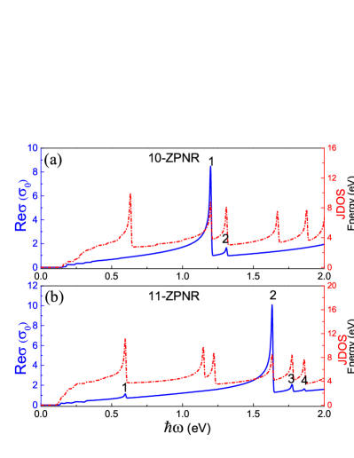
Figure 6 shows the intra-band JDOS [(red) dash-dotted line] and optical absorption spectrum [(blue) solid line] for (a) 10-ZPNR and (b) 11-ZPNR with the corresponding band structures and Fermi levels shown in (c) and (d), respectively. As depicted in Fig. 6(a), the first JDOS peak for 10-ZPNR located at 0.604 eV comes from the transition between the =6 subband and the =5 one. But there is no absorption peak at the same frequency because the parities of the two subbands are different [see Fig. 6(c)] and the transitions are forbidden by the symmetry. In other words, this transition violates the intra-band optical transition selection rule (=even) for even- ZPNRs. By the same token, the second and third JDOS peaks are contributed by the transitions between the subbands with the same parities [see Fig. 6(c)], hence the corresponding absorption peaks appear [see the (blue) solid line]. On the contrary, we find that the optical absorption peaks are almost presented for 11-ZPNR [see Fig. 6(b)] arising from the symmetry breaking which means that the all optical transitions are principally possible among all subbands. The corresponding transitions are shown in Fig. 6(d). On the other hand, some of the matrix elements may be tiny (weak), i.e, the , and the corresponding absorption peaks are missing in this case [see Fig. 6(b)].
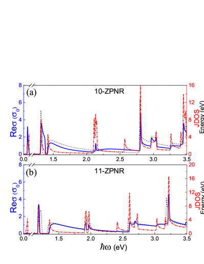
Next, we turn to the effect of externally applied electric field on the optical property of ZPNRs. Fig. 7 depicts the inter-band JDOS [(red) dash-dotted line] and optical absorption spectra [(blue) solid line] for (a) 10-ZPNR and (b) 11-ZPNR under a uniform vertical electric field (VEF) with strength =0.1V/, where the corresponding band structures with the optical transition indications are shown in (c) and (d), respectively. The Fermi level for both cases are lying between the edge states. In real experiment, the VEF corresponding to the top gate or substrate effect. It maybe be generated by using the polar semiconductors interface Dong Zhang . Owing to the puckered lattice structure of ZPNRs, the band structure of the ZPNR under a VEF is even-odd dependent Zhoubl since the edge states of even (odd)- ribbons located on the different (same) sub-layers. The VEF opens a gap between the two edge bands for even ribbons [see Fig. 7(c)], but for odd ones the two edge bands are always (nearly) degenerated [see Fig. 7(d)]. Further, the VEF also breaks the symmetry in even- ZPNRs. These features are also reflected in the optical absorption spectrum. From Fig. 7(a), we find that several extra absorption peaks [the (blue) solid line] appear due to the symmetry breaking by the VEF compared with the bare 10-ZPNR [see the (black) dashed line]. Especially, the first absorption peak in mid-infrared frequency is greatly enhanced due to the degeneracy lifting of the edge states. In comparison, as shown in Fig. 7(b), the absorption spectrum of 11-ZPNR is slightly changed compared to the bare case [also see the (black) dashed line] since the band structure is nearly unaffected by the VEF. These features offer a useful approach to identify the even-odd property of ZPNR samples by experimentally detecting the optical absorption under VEF.
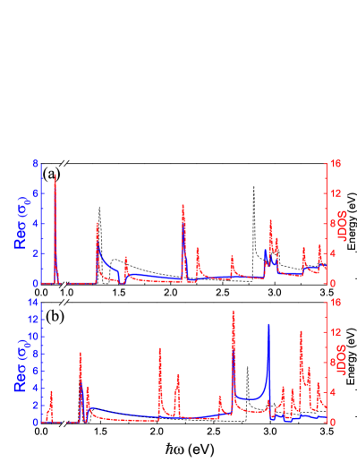
Experimentally, it is difficult to avoid impurities and defects in samples. This may consequently affect the optical properties of ZPNRs by changing the band structure or breaking the symmetry. Figs. 8 (c) and 8(d) show the band structure of 10-ZPNR with impurities distributing on its one edge (the 1st atomic row) and the center (the 10th row), respectively, where we have defined a -ZPNR with 2 atomic rows. For a zigzag chain of ZPNR there are two phosphorus atomic rows, hence a -ZPNR has 2 rows. We model the impurity effect by adding a impurity potential to the on-site energy of the corresponding impurity atoms, which is widely used in previous works zouyl ; L.L.Li . As shown in Fig. 8(c) for impurities located on the edge, we find that the nearly degenerated edge states are separated [see the (orange) solid line] due to the variation of the on-site energies, but the other subbands remain unchanged. This is consistent with the result obtained by the first-principles calculation Pooja ; guocx . On the contrary, comparing Fig. 8(d) with Fig. 3(a), as impurities localized on the center the subband contributed by the impurities are shifted [see the (orange) solid line] but the other subbands remain unchanged. This means that the impurities only have a local effect on the electronic structure of a ZPNR. But, they will play an important role in the optical absorption spectrum because of the lattice symmetry breaking. Figs. 8(a) and 8(b) show the inter-band JDOS [(red) dash-dotted line] and optical absorption spectrum [(blue) solid line]for 10-ZPNR with impurities located at its one edge (the 1st atomic row) with =-0.1954 eV and the center (the 10th row) with 0.3058 eV, respectively. The impurities localized at the edge break the symmetry since the wavefunctions corresponding to most of the subbands are partially distributed on the edge. Hence, we observe the first and some extra optical absorption peaks reappeared [see the (blue) solid line] compared with the pristine 10-ZPNR shown in Fig. 8(a) [(black) dash line]. This is similar to that of the VEF effect discussed above. Similarly, from Fig. 8(b), we also find some extra peaks when the impurities localized at the center. However, the absorption peak at the mid-infrared frequency (the first peak) is still missing although the symmetry is broken in this case. The reason is that the edge states are mainly localized on the edge atoms, in consequence the band structure is nearly unaffected by the impurities localized on the center atoms. For 11-ZPNR, the optical absorption spectrum is just slightly changed by the impurities, hence we do not present the result here for saving space.
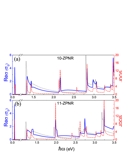
Finally, a transverse electric field (TEF) can induce a Stark effect (potential difference) arising from the finite width of ZPNRs ezawa , which can make a significant change of the band structure, especially the edge bands. And this effect has been experimentally observed for few-layer BPs BingchenDeng . As a result, this can also change the optical properties of ZPNRs by breaking the symmetry. Therefore, Fig. 9 displays the inter-band JDOS [(red) dash-dotted line] and optical absorption spectrum [(blue) solid line] for (a) 10-ZPNR and (b) 11-ZPNR under a uniform TEF with strength =0.008 V/. And the corresponding band structures are shown in Figs. 9(c) and 9(d), respectively. As shown in the figure, we find that in the presence of the TEF the optical absorption peaks are shifted compared to the bare ribbons [see the (black) dashed line]. In Figs. 9(c) and 9(d), unlike the VEF case, we can see the degeneracy of the edge states for 10- and 11-ZPNR are both lifted by the Stark effect. Owing to the symmetry breaking, all possible absorption peaks in 10-ZPNR corresponding to the JDOS appear [see Fig. 9(a)], which means that the optical absorption of 10-ZPNR is greatly enhanced, especially the absorption peak in the mid-infrared frequency. Further, the first absorption peak for both 10- and 11-ZPNR is greatly enhanced due to the degeneracy lifting as show in Figs. 9(a) and 9(b). Hence we conclude that the effect of TEF on the optical absorption in ZPNRs is different from that of the VEF or impurity. A TEF can induce different potentials on all atoms within a super-cell, which leads to a global symmetry breaking.
IV Summary
In summary, we have theoretically studied the electronic and optical properties of ZPNRs under a linearly polarized light along the longitudinal direction based on the TB Hamiltonian and Kubo formula. We have obtained analytically the energy spectra of ZPNRs and the optical transition selection rules based on the lattice symmetry analysis. Owing to the symmetry, the eigenstates of even- ZPNRs are transversely either symmetric or antisymmetric, which makes their optical response qualitatively different from that of the odd- ones. In particular the inter (intra) -band selection rule for even- ZPNRs is odd (even) since the parity factor of the wavefunction corresponding to the conduction (valence) band is (with the subband index ) provided by the symmetry. For odd- ZPNRs, however, the all optical transitions are possible among all subbands. Further, the edge states play an important role in the optical absorption and are involved in many of the absorption peaks. The optical absorption of even- ZPNRs can be enhanced by the substrate and impurity effect as well as the transverse electric field via breaking the symmetry. While the optical absorption of odd- ones can be effectively tuned by lattice defects or external electric fields. Our findings provide a further understanding on the electronic states and optical properties of ZPNRs, which are essential for the explanation of the optical experiment data on ZPNR samples.
V Acknowledgments
This work was supported by the National Natural Science Foundation of China (Grant Nos. 11804092, 11774085, 61674145, 11704118, 11664010), and China Postdoctoral Science Foundation funded project Grant No. BX20180097, and Hunan Provincial Natural Science Foundation of China (Grant No. 2017JJ3210).
Appendix A
In this appendix, we calculate the optical transition matrix elements in Eq. (24). Utilizing the relation combined the wavefunction in Eq. (18), the optical matrix element can be written as Peteryu
| (A1) |
is the wavefunction in Eq. (18) or (19). According to Eq. (18), the transition matrix element between the bulk states is
| (A2) | ||||
where is the atom site index, and indicates the parity of the subbands. There are five hoppings, including for , for , for , for , and for . Then, Eq. (A2) can be written as
| (A3) |
where , and represent the term of transition matrix related to the hopping , and , and the corresponding term can be written as
| (A4) | ||||
where the sum of runs from to . Defining, , we find also runs from to when . Applying the summation transform , can be rewritten as
| (A5) | ||||
Meanwhile, the term is
| (A6) | ||||
in this case, the atoms at the edges should be excluded because the hopping links of is beyond one zigzag chain. Applying similar summation transform in to , we have
| (A7) | ||||
Finally, the term is
| (A8) | ||||
Here, we have used the relation to simplify it. Similarly, replacing all the summation index with , we obtain
| (A9) | ||||
Therefore, the transition matrix elements is
| (A10) |
where
From Eq. (A10), we can explicitly find that only the inter band transition between the bulks states with the same symmetry are allowed. Using the wavefunction in Eq. (19), we can obtain the same selection rules for the transition between the edge bands as well as the bulk bands to the edge bands. Hence, in even- ZPNRs, we conclude that only the transitions between the subbands with same parity are allowed.
References
- (1) Likai Li, Yijun Yu, Guojun Ye, Qingqin Ge, Xuedong Ou, Hua Wu, Donglai Feng, Xian Hui Chen, and Yuanbo Zhang, Nat. Nanotech. 9, 372 (2014).
- (2) Han Liu, Adam T. Neal, Zhen Zhu, Zhe Luo, Xianfan Xu, David Tománek, and Peide D. Ye, Acs Nano. 8, 4033 (2014).
- (3) Fengnian Xia, Han Wang, and Yichen Jia, Nat. Commun. 5, 4458 (2014).
- (4) Steven P. Koenig, Rostislav A. Doganov, Hennrik Schmidt, A. H. Castro Neto, and Barbaros Özyilmaz, Appl. Phys. Lett. 104, 103106 (2014).
- (5) Michele Buscema, Dirk J. Groenendijk, Sofya I. Blanter, Gary A. Steele, Herre S. J. van der Zant, and Andres Castellanos-Gomez, Nano Lett. 14, 3347 (2014).
- (6) Andres Castellanos-Gomez, Leonardo Vicarelli, Elsa Prada, Joshua O Island, K L Narasimha-Acharya, Sofya I Blanter, Dirk J Groenendijk, Michele Buscema, Gary A Steele, J V Alvarez, Henny W Zandbergen, J J Palacios, and Herre S J van der Zant, 2D Mater. 1, 025001 (2014).
- (7) Wanglin Lu, Haiyan Nan, Jinhua Hong, Yuming Chen, Chen Zhu, Zheng Liang, Xiangyang Ma, Zhenhua Ni, Chuanhong Jin, and Ze Zhang, Nano. Res. 7, 853 (2014).
- (8) Xiaomu Wang, Aaron M. Jones, Kyle L. Seyler, Vy Tran, Yichen Jia, Huan Zhao, Han Wang, Li Yang, Xiaodong Xu, and Fengnian Xia, Nat. Nanotech. 10, 517 (2015).
- (9) Xi Ling, Han Wang, Shengxi Huang, Fengnian Xia, and Mildred S. Dresselhaus, PNAS 112, 4523 (2015).
- (10) Andres Castellanos-Gomez, J. Phys. Chem. Lett. 6, 4280 (2015).
- (11) Likai Li, Jonghwan Kim, Chenhao Jin, Guojun Ye, Diana Y. Qiu, Felipe H. da Jornada, Zhiwen Shi, Long Chen, Zuocheng Zhang, Fangyuan Yang, Kenji Watanabe, Takashi Taniguchi, Wencai Ren, Steven G. Louie, Xianhui Chen, Yuanbo Zhang, and Feng Wang, Nat. Nanotech. 12, 21 (2017).
- (12) Sherman Jun Rong Tan, Ibrahim Abdelwahab, Leiqiang Chu, Sock Mui Poh, Yanpeng Liu, Jiong Lu, Wei Chen, and Kian Ping Loh, Adv. Mater. 30, 1704619 (2018).
- (13) A. S. Rodin, A. Carvalho, and A. H. Castro Neto, Phys. Rev. Lett. 112, 176801 (2014).
- (14) X.Y. Zhou, R. Zhang, J. P. Sun, Y. L Zou, D. Zhang, W. K. Lou, F. Cheng, G. H. Zhou, F. Zhai, and Kai Chang, Sci. Rep. 5, 12295 (2015).
- (15) Xiaoying Zhou, Wen-Kai Lou, Feng Zhai, and Kai Chang, Phys. Rev. B 92, 165405 (2015).
- (16) R. Zhang, X. Y. Zhou, D. Zhang, W. K. Lou, F. Zhai, and K. Chang, 2D Mater. 2, 045012 (2015).
- (17) Xiaoying Zhou, Wen-Kai Lou, Dong Zhang, Fang Cheng, Guanghui Zhou, and Kai Chang, Phys. Rev. B 95, 045408 (2017).
- (18) Tony Low, A. S. Rodin, A. Carvalho, Yongjin Jiang, Han Wang, Fengnian Xia, and A. H. Castro Neto, Phys. Rev. B 90, 075434 (2014).
- (19) Vy Tran and Li Yang, Phys. Rev. B 89, 245407 (2014).
- (20) Rui Zhang, Zhenhua Wu, X. J. Li, and Kai Chang, Phys. Rev. B 95, 125418 (2017).
- (21) A. N. Rudenko and M. I. Katsnelson, Phys. Rev. B 89, 201408(R) (2014).
- (22) A. N. Rudenko, Shengjun Yuan, and M. I. Katsnelson, Phys. Rev. B 92, 085419 (2015).
- (23) A. Carvalho, A. S. Rodin, and A. H. Castro Neto, Europhys. Lett. 108 47005 (2014).
- (24) Xiaoyu Han, Henry Morgan Stewart, Stephen A. Shevlin, C. Richard A. Catlow, and Zheng Xiao Guo, Nano Lett. 14, 4607 (2014).
- (25) M. Ezawa, New J. Phys. 16, 115004 (2014).
- (26) Esmaeil Taghizadeh Sisakht, Mohammad H. Zare, and Farhad Fazileh, Phys. Rev. B 91, 085409 (2015).
- (27) Nourbakhsh Zahra and Asgari Reza, Phys. Rev. B 94, 035437 (2016).
- (28) Longlong Zhang and Yuying Hao, Sci. Rep. 8, 6089 (2018).
- (29) H. Guo, N. Lu, J. Dai, X. Wu, and X. C. Zeng, J. Phy. Chem. C 118, 14051 (2014).
- (30) Paul Masih Das, Gopinath Danda, Andrew Cupo, William M. Parkin, Liangbo Liang, Neerav Kharche, Xi Ling, Shengxi Huang, Mildred S. Dresselhaus, Vincent Meunier, and Marija Drndić, ACS Nano, 10, 5687 (2016).
- (31) Yudai Nakanishi, Ayumi Ishi, Chika Ohata, David Soriano, Ryo Iwaki, Kyoko Nomura, Miki Hasegawa, Taketomo Nakamura, Shingo Katsumoto, Stephan Roche, and Junji Haruyama, Nano Res. 10, 718 (2017).
- (32) Zhili Zhu, Chong Li, Weiyang Yu, Dahu Chang, Qiang Sun, and Yu Jia, Appl. Phys. Lett. 105, 113105 (2014).
- (33) Guang Yang, Shenglong Xu, Wei Zhang, Tianxing Ma, and Congjun Wu, Phys. Rev. B 94, 075106 (2016).
- (34) Yi Ren, Fang Cheng, Z. H. Zhang, and Guanghui Zhou, Sci. Rep. 8, 2932 (2018).
- (35) E. Taghizadeh Sisakht, F. Fazileh, M. H. Zare, M. Zarenia, and F. M. Peeters, Phys. Rev. B 94, 085417 (2016).
- (36) Benliang Zhou, Benhu Zhou, Xiaoying Zhou, and Guanghui Zhou, J. Phys. D: Appl. Phys. 50, 045106 (2017).
- (37) Sima Shekarforoush, Daryoush Shiri and Farhad Khoeini, arXiv: 1802.02065.
- (38) R. Ma, H. Geng, W. Y. Deng, M. N. Chen, L. Sheng and D. Y. Xing, Phys. Rev. B 94, 125410 (2016).
- (39) Datta S, Quantum Transport-Atom to Transistor, Cambridge University Press, (2005).
- (40) Katsunori Wakabayashi, Ken-ichi Sasaki, Takeshi Nakanishi, and Toshiaki Enoki, Sci. Technol. Adv. Mater. 11, 054504 (2010).
- (41) V. A. Saroka, M. V. Shuba, and M. E. Portnoi, Phys. Rev. B 95, 155438 (2017).
- (42) M. Aminic and M. Soltani, arXiv: 1810.03042.
- (43) Mahdi Moradinasab, Hamed Nematian, Mahdi Pourfath, Morteza Fathipour, and Hans Kosina, J. Appl. Phys. 111, 074318 (2012).
- (44) Tsuneya Ando, and Yasutada Uemura, J. Phys. Soc. Jpn. 36, 959 (1974).
- (45) Mikito Koshino and Tsuneya Ando, Phys. Rev. B 77, 115313 (2008).
- (46) M G Burt, J. Phys.: Condens. Matter 4, 6651 (1992).
- (47) Ruo-Yu Zhang, Ji-Ming Zheng, and Zhen-Yi Jiang, Chin. Phys. Lett. 35, 017302 (2018).
- (48) Weifeng Li, Gang Zhang, and Yong-Wei Zhang, J. Phys. Chem. C 118, 22368 (2014).
- (49) Li-kun Shi, Kai Chang, and Chang-Pu Sun, arXiv:1601.04722.
- (50) Ting Cao, Meng Wu, and Steven G. Louie, Phys. Rev. Lett. 120, 087402 (2018).
- (51) Peter Y. Yu, and Manuel Cardona, Fundamentals of Semiconductors Physics and Materials Properties 4ed, Springer (2010).
- (52) Han Hsu and L. E. Reichl, Phys. Rev. B 76, 045418 (2007).
- (53) H. C. Chung, M. H. Lee, C. P. Chang, and M. F. Lin, Opt. Express 19, 23350 (2011).
- (54) Dong Zhang, Wenkai Lou, Maosheng Miao, Shou-cheng Zhang, and Kai Chang, Phys. Rev. Lett. 111, 156402 (2013).
- (55) Yong-Lian Zou, Juntao Song, Chunxu Bai, and Kai Chang, Phys. Rev. B 94, 035431 (2016).
- (56) L. L. Li and F. M. Peeter, Phys. Rev. B 97, 075414 (2018).
- (57) Pooja Srivastava, K. P. S. S. Hembram, Hiroshi Mizuseki, Kwang-Ryeol Lee, Sang Soo Han, and Seungchul Kim, J. Phys. Chem. C 119, 6530 (2015).
- (58) Caixia Guo, Congxin Xia, Lizhen Fang, Tianxing Wang and Yufang Liu, Phys. Chem. Chem. Phys. 18, 25869 (2016).
- (59) Bingchen Deng, Vy Tran, Yujun Xie, Hao Jiang, Cheng Li, Qiushi Guo, Xiaomu Wang, He Tian, Steven J. Koester, Han Wang, Judy J. Cha, Qiangfei Xia, Li Yang, and Fengnian Xia, Nat. Commun. 8, 14474 (2017).