Field-induced insulating states in a graphene superlattice
Abstract
We report on high-field magnetotransport ( up to 35 T) on a gated superlattice based on single-layer graphene aligned on top of hexagonal boron nitride. The large-period moiré modulation ( nm) enables us to access the Hofstadter spectrum in the vicinity of and above one flux quantum per superlattice unit cell ( at T). We thereby reveal, in addition to the spin-valley antiferromagnet at , two insulating states developing in positive and negative effective magnetic fields from the main and quantum Hall states respectively. We investigate the field dependence of the energy gaps associated with these insulating states, which we quantify from the temperature-activated peak resistance. Referring to a simple model of local Landau quantization of third generation Dirac fermions arising at , we describe the different microscopic origins of the insulating states and experimentally determine the energy-momentum dispersion of the emergent gapped Dirac quasi-particles.
I Introduction
Van der Waals assembly of atomically-thin materials represents a novel powerful strategy for the realization of artificial structures with tailored electronic response.Geim_13 Inherent to this approach is the control of the crystallographic orientation of the atomic layers, a novel degree of freedom that can profoundly alter the electrostatic landscape experienced by the charge carriers. The stack of graphene Novoselov_04 on top of hexagonal boron nitride (hBN),Dean_10 and the subsequent reconstruction of the electronic spectrum hosting ’second generation’ Dirac cones,Yankowitz_12 is a prototypical case. The small lattice mismatch (%) between their isomorphic structures results into an hexagonal superlattice modulation (so-called moiré pattern),Xue_11 ; Decker_11 ; Yankowitz_12 which sets an artificial periodicity as large as nm for perfect crystallographic alignment. This twist-dependent superstructure, combined with the possibility of in-situ tuning of the band filling via electrostatic field-effect, has made graphene-hBN superlattices the ideal platform for the experimental study of the Hofstadter butterfly (HB).Hofstadter_76 ; Ponomarenko_13 ; Dean_13 ; Hunt_13 The HB is the fractal (i.e. recursive, self-similar) energy spectrum acquired by a two-dimensional (2D) electronic system when simultaneously subjected to (i) a periodic electrostatic potential (the hexagonal moiré in our case) and (ii) a perpendicular magnetic field.Hofstadter_76 A spatially periodic potential groups the electronic states into discrete Bloch bands;Ashcroft a perpendicular magnetic field quantizes the electronic spectrum into Landau levels.Kittel These fundamental effects can usually be treated independently, however under particular circumstances the two quantizations combine into the HB. This happens when rational values of magnetic flux quanta () threads the superlattice unit cell, i.e. when (where is the total magnetic flux, is the superlattice unit cell area, the Planck constant, the electron’s charge). Thereby, the Bloch (Landau) bands splits into () sub-bands, leading to a repeated ’cloning’ of the original magnetic spectrum.Hofstadter_76
In the case of graphene superlattices, the HB combines with the specific response of graphene’s 2D Dirac fermions to large magnetic fields.Novoselov_05 ; Zhang_05 When tuned to charge neutrality, graphene systems exhibits a field-induced insulating state which has been a subject of intensive experimental study in single-layer,Zhang_06 ; Checkelsky_07 ; Giesbers_09 ; Du_09 ; Yu_13 ; Young_14 bilayerFeldman_09 ; Freitag_12 ; Velasco_12 ; Maher_13 ; Pezzini_14 and multi-layers.Bao_11 ; Grushina_15 This state arises at half filling of the zero-energy Landau level (LL) - a unique signature of Dirac fermions - and has an interaction-induced origin based on the so-called quantum Hall (QH) ferromagnetism (QHFM), i.e. on the formation of spin-valley polarized states at partial LL fillings.Young_12 It is therefore of fundamental interest to understand if ’copies’ of this state are present in graphene’s HB, and in which way their phenomenology does differ from the ’original’ one. Using capacitance spectroscopy Yu et al. already showed evidence for QHFM in graphene superlattices.Yu_14 However, magneto-capacitance is sensitive only to the bulk density of states and does not allow discerning between QH and insulating states. On the other hand, electrical transport can be employed to identify insulating phases with an energy gap for both the bulk and edge excitations. Bearing this in mind, we have investigated a 15 nm graphene-hBN superlattice with high-field temperature-dependent magnetotransport measurements. By this means, we reveal three field-induced insulating states in the HB and quantitatively estimate their activation energies and the gaps’ field dependence. Their microscopic origin is interpreted in connection to the emergence of so-called ’third generation’ Dirac particles, i.e. field-and-superlattice-induced replica, experiencing zero effective magnetic field when (i.e. at T for our superlattice). By analyzing their local Landau quantization, we reveal a significant renormalization in the Fermi velocity of the corresponding gapped Dirac cones.
II Experimental methods
We studied a six-terminal Hall bar device ( m2), defined by reactive ion etching and evaporation of Cr/Au contacts. The sample is based on a stack of single-layer graphene on top of a 50 nm thick hBN crystal, obtained with a dry van der Waals assembly technique.Kretinin_14 Straight edges of the two crystals are aligned within during the assembly (giving a 50% success chance of crystallographic alignment due to the uncertainty on the zig-zag or armchair nature of the selected edges). The measurements presented were performed in a 4He-flow cryostat (base temperature 1.5 K), inserted in the access bore of a resistive Bitter magnet at the High Field Magnet Laboratory (HFML-EMFL). The resistance was measured with low-frequency lock-in detection, both in two and four-probe configuration, with a constant ac voltage of 10 mV applied to the sample connected in series to a 100 k resistor.
III Results and Discussion
III.1 Hofstadter butterfly
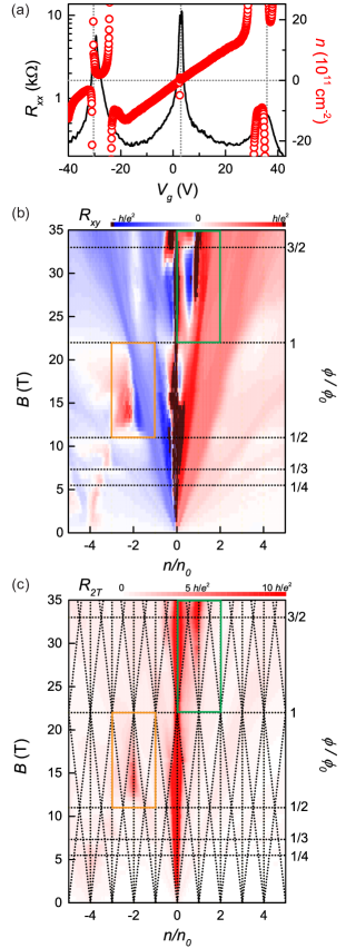
The black trace in Fig.1 (a) shows the four terminal resistance of our device () as a function of gate voltage (, applied to the underlying Si/SiO2 substrate), measured at T and K. As expected for an aligned graphene-hBN stack, three pronounced peaks are visible. At V the Fermi level is set at the touching between the conduction and valence band Dirac cones. The peak value of the resistance at this point remains k (slightly varying over different cooldowns), indicating that no appreciable band-gap opens in the absence of a magnetic field. The two additional maxima symmetrically located at large positive (negative) doping V, on the other hand, correspond to half filling of second generation Dirac mini-bands induced by the superlattice potential.Yankowitz_12 To confirm this identification, we measured the Hall resistance as a function of at low magnetic field ( T, avoiding quantization effects) and extracted the corresponding 2D carrier density (red open circles in Fig.1 (a)). Close to V, changes its sign as the system is set to the charge neutrality point (CNP), while it varies linearly with otherwise, with a slope cm-2/V. Further away from the main CNP, changes its sign a first time at the onset of the superlattice mini-bands ( V, corresponding to van Hove singularities,Wallbank_13 ) and a second time at V, indicating the CNPs for the superlattice-induced Dirac mini-bands. Due to the spin and valley degeneracy, these satellite CNPs are realized when accommodating four electrons per superlattice unit cell, i.e. when cm-2, with . The positioning of the satellite peaks therefore allows to estimate a periodicity nm for the hexagonal moiré pattern, which confirms the high degree of crystallographic alignment between the graphene and hBN crystals.
In Fig.1 (b) we present a colour map of the Hall resistance as function of magnetic field (0 T T) and carrier density per superlattice unit cell (corresponding to the same range of used in (a)). The red areas indicate electron doping, the blue ones hole doping, while in the black ones exceeds , typically signalling a divergence due to a CNP. On top of the standard Landau fan diagram of single-layer graphene (with full degeneracy lifting of the LL), one can clearly identify a recursive pattern due to the HB. This is particularly evident in the lower-left part of the map, which is dominated by a series of charge conversions and local Landau mini-fans. These features are understood in terms of the formation of -fold degenerate Zak mini-bands,Zak_64 which are in fact gapped Dirac cones,Chen_14 and experience zero effective field when . The emergent third generation Dirac quasi-particles are then subjected to Landau quantization in a finite (positive or negative) effective magnetic field . The appearance of these structures have a clear periodicity, with a characteristic frequency T, that provides an alternative way to estimate the moiré periodicity nm, in reasonable accordance with the value given above.
III.2 Insulating regions within local Landau fans
Within the HB, a simple Diophantine relation (with , integer numbers, although fractional indices were recently reported in Refs.Wang_15, ; Spanton_17, ) locates the expected incompressible (i.e. bulk-gapped) states in the flux-density space. The slope can be seen as a generalized filling factor and actually defines the expected Hall conductivity , while indicates the amount of filling of the Bloch bands. In Fig.1 (c) we plot a grid of lines, i.e. a so-called Wannier diagram,Wannier_78 limited to only, on top of a color map of the two-terminal resistance of our device . For convenience and better visibility we use (rather than the four-terminal resistance ) in this color map; however, all the quantitative analysis later on will be performed using quantities not affected by the contact resistance, i.e. , and . In this graph, we can conveniently identify different regions in the field-gate space in which the device becomes strongly resistive. These regions disperse as , i.e. as vertical lines in the Wannier diagram, and appear to be strongly modulated by the gaps, which enclose regions of Landau filling . The first insulating area at (reaching a maximum two terminal resistance M, and four terminal resistance M, at K) extends over the whole field range and corresponds to half filling of the main LL. A second insulating state ( M, M) is located at and develops for T, i.e. in T (green box). A third (weaker) one ( M, 70 k) develops at for T, i.e. for (orange box). By comparison with Fig.1 (b), it is evident that all the three insulating states also correspond to changes in the sign of , marking the boundary between local electron-doped and hole-doped regions. However, not every change in the carrier sign corresponds to insulating regions: notably, the satellite NPs do not develop into -induced insulating state due to overlap with the robust Landau gaps from the main neutrality point. On the other hand, the -induced insulating states do not coexist with any state from main QH fan, which makes them observable in our experiment. The competition with Landau gaps developing in the same field-density region evidently constrains the possibility to experimentally access the insulating states. In addition, our experiment reveals a pronounced electron-hole asymmetry in the HB (see Figure 1 (b)), clearly affecting the second and third insulating states, for which we did not find a particle-hole symmetric. This asymmetry was consistently seen in previous experiments on graphene-hBN superlattices Ponomarenko_13 ; Dean_13 ; Hunt_13 and reproduced by calculations.Wallbank_13 ; Chen_14 The superlattice perturbation induced by an hexagonal substrate having inequivalent sublattice sites (i.e. hosting Boron and Nitrogen atoms) is considered responsible for this effect.DaSilva_15
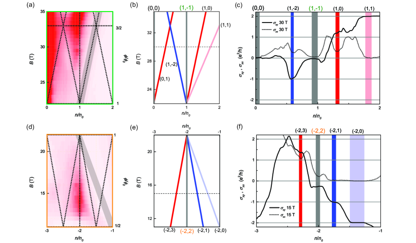
In the following, we use the notation (,)Yu_14 in order to label the incompressible states in the local fan diagrams and check the consistency of the two -induced insulating states within the Hofstadter picture. Here is the filling factor of the ‘parent’ QH state, while is the filling factor in the local Landau fan. The relations and necessarily hold. Figure 2 (a) shows an enlarged view of the , region, centred on the (1,-1) insulating state. The index is given by the main QH state located at for T, i.e. (shaded area). This QH state determines the energy gap for the third generation Dirac particles at , . The local QH fan, resulting from occupation of single-degenerate local LLs, is shown in Fig.2 (b) (along with the neighbouring one, which develops from the main state). The colour code corresponds to the expected value for the Hall conductivity, given by , (grey , blue , red , light blue , light red ). Panel (c) shows line traces of and at T ( T), which matches the expectation of the local fan diagram in (b). Although this pattern was reproducible over several cool-downs, the accuracy in the quantization of and was found to vary as a result of thermal cycling (e.g., the state (0,1), which cannot be identified here, was close to quantization in a previous measurement session). As shown in panels (d-f), the same analysis is successfully applied to the (-2,2) insulating state in the , region, which corresponds to a main filling factor , although the quantization at T is found to be generally less accurate than in the previous case.
III.3 Energy gaps and microscopic origin
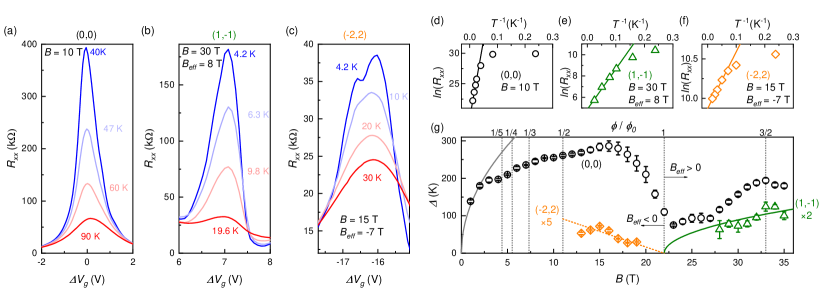
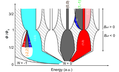
Having rationalised the presence of the (1,-1) and (-2,2) states in the graphene’s HB, it is worthwhile to compare our observations with the existing experimental literature on the subject. In particular, Yu et al. already identified both (1,-1) and (-2,2) states as incompressible in capacitance measurements,Yu_14 while Hunt et al. showed vanishing two-terminal conductance both at (1,-1) and its particle-hole symmetric (-1,1).Hunt_13 Moreover, by carefully inspecting the colour plots in Ref.Wang_15, , one can spot even a larger number of such highly resistive regions. However, quantitative information on the amplitude of the energy gaps and its connection to the physical origin of these states is still missing. Thereby, we measured () in the vicinity of the three insulating states (0,0), (1,-1) and (-2,2), for increasing temperatures and different magnetic fields, with steps of 1 T. Typical () traces for the three states, at representative values of and fixed (), are plotted in Fig.3 (a-c). The insulating temperature dependence, i.e. the peak in increasing with decreasing temperature and exceeding , is evident in the three panels. We then analysed these data by fitting an Arrhenius type behaviour () to the -dependence at fixed values of ( is the energy gap and the Boltzmann constant), which is clearly emphasized in ln() vs 1/ plots, as shown in Fig.3 (d-f). Typically, this exponential dependence applies to relatively high temperature ranges, while saturates at low , where it results from hopping between localized states inside the energy gap. In Fig.3 (g) we show the complete field dependence of the energy gaps of the three insulating states, obtained by fits of the kind shown by solid lines in panels (d-f); the error bars are given by the standard error in the fitting parameter . We discuss this panel by referring to the schematic diagram of Fig.4, which shows a simple model of Landau quantization for the third generation Dirac fermions and the resulting energy gaps.Chen_14 ; Yu_14 The main LLs are represented as dashed areas; in accordance to the experimental observations (see Fig.1 (b)), the main LL splits into four branches, while the retains the four-fold degeneracy. The states relevant to our discussion are colour-filled, with a code intended to match the plots of Fig.2.
The (0,0) insulating state extends over the entire field range considered in our experiment. Its energy gap can be estimated to be in the order of 150 K (14 meV) already at T (see open circles in Fig.3 (g)). This energy scale is well beyond the single-particle spin splitting determined by the Zeeman energy [KT-1] (where is the Landé factor, the Bohr magneton). It is instead comparable to the Coulomb energy [KT-1/2] (where is the magnetic length and the relative dielectric constant), which is plotted as a grey solid line in Fig.3 (g), assuming for the non-encapsulated graphene-hBN sample used in this experiment.Dean_11 This observation is consistent with the formation of a spin-valley antiferromagnetic order at half filling of the LL,Kharitonov_12 in which electrons with opposite spin polarization occupy the two sublattice sites, minimizing the Coulomb repulsion.Young_14 The energy gap shows a markedly non-monotonic behavior as a function of magnetic field: it grows in the range 1 T T (although significantly deviating from from 4 T on), it strongly decreases for 16 T T, and finally increases again up to the highest fields applied. We attribute the deviation from to the fact that resistance data at relatively high temperature (up to K) were necessary to estimate . At such temperatures the Zak mini-bands arising at rational values of flux quanta, recently identified in a new kind of quantum oscillatory phenomenon,Kumar_17 ; Kumar_18 compete with the thermally-excited conductivity across the gap, partially hindering the exponential dependence of . The dramatic suppression of the gap in the second region is due to the exponential broadening of the split LLs caused by the superlattice modulation, which reaches its maximum at , where the band edges correspond to gapped Dirac cones.Wallbank_13 Local LL quantization in yields to the opening of a state, which is reflected by the final increase in (0,0). These findings are fully consistent with previous magneto-capacitance spectroscopy measurements.Yu_14
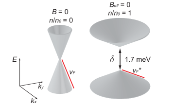
The gap for the (1,-1) insulating state (open green triangles in Fig.3 (g)) is sizeable for T ( T), increases monotonically with the field, and it is best fitted by a -dependence. The parent quantum Hall state in this case is the , (1,0) in the local notation. Its gap is known to be determined by the energy cost for the formation of skyrmionic spin textures,Young_12 which is proportional to . The is found to extend continuously from T (see Fig.1 (b)), without experiencing any gap-closing, which was instead reported at in Ref.Yu_14, . The fact that (1,0) remains gapped at (with (1,0)( T) K) is attributed to the smaller dielectric constant in our non-encapsulated sample, which enhances the interaction effects in comparison to the case of fully encapsulated structures (), like the capacitance device use in Ref.Yu_14, . On the other hand, the (1,-1) state results from full depletion of a single-degenerate - like local Landau level. Thereby, it is safe to assume that this insulating state has a single-particle origin, i.e. that it corresponds to the first cyclotron gap in the local single-degenerate Landau fan (see corresponding grey area in Fig.4), which amplitude is given by . Our best fit [KT-1/2] can therefore provide a way to estimate the Fermi velocity of the corresponding third generation Dirac fermions . However, it is well known that the experimental activation gap for the equivalent state in the conventional graphene spectrum (), although extremely large,Novoselov_07 highly underestimates the theoretical cyclotron gap. To circumvent this issue, we measured the activation gap of the (-2,0) state in our sample at T, where full quantization is already achieved and superlattice effects are minimized, and obtained T) K (theoretical value 590 K). We then estimated from the ratio . The direct comparison between two states with the same microscopic origin, i.e. first cyclotron gap in the Dirac spectrum, respectively in an effective and absolute field, is intended to take into account the sample-dependent localization mechanism that is responsible for the bulk gaps in the quantum Hall regime. Our analysis gives , i.e. it indicates a significant renormalization of the band dispersion for the field-and-superlattice-induced Dirac fermions with respect to the ones of standard single-layer graphene ( m/s). A schematic comparison is presented in Fig.5.
Finally, the field-dependence of the activation gap for the (-2,2) state is presented as open orange diamonds in Fig.3 (g). This state appears to be less robust then the ones discussed above. This is reflected by its complete suppression at , while the other insulating states remain sizeable at and beyond. The single (quasi) quantized steps of in the vicinity of (-2,2) (see Fig.2 (f)) indicate that the degeneracy of the four-fold local LL for the replica Dirac fermions is fully lifted in negative (see Fig.4). The (-2,2) state corresponds to half-filling of this level, i.e. it is analogous to the (0,0) presented above. However, its gap is far from being comparable to and it is best fitted by (-2,2)[KT-1], which can be attributed to Zeeman splitting in an effective magnetic field, with an enhanced Landé factor . This kind of -dependence for the gap at half filling of the LL was typically reported for disordered graphene samples on SiO2,Giesbers_09 while a much larger renormalized was estimated for graphene on hBN in Ref.Young_12, . Despite the low-disorder environment guaranteed by the graphene/hBN stack, our observations indicate a moderate contribution of e-e interaction to the degeneracy lifting in this local Landau fan. Further experimental data would be however necessary to determine the exact microscopic ordering underlying the (-2,2) state; tilted-field experiments allowing for an independent tuning of the Zeeman field could be of particular relevance.
IV Conclusions and Outlook
In summary, we have presented a study of temperature-dependent magnetotransport on a graphene-hBN superlattice with 15 nm moiré periodicity. The electrical transport experiments allows the identification of three fully gapped regions in the HB. These states, despite sharing a common insulating nature, can be traced to different microscopic origin within the main QH spectrum of single-layer graphene and its replica in the vicinity of ( T). Importantly, our analysis identifies the insulating state (1,-1) as corresponding to the first cyclotron gap in the local Landau fan of the replica Dirac fermions. The -dependence of its gap, in combination with knowledge of the gap at 22 T, enables to experimentally determine the energy-momentum dispersion of the corresponding superlattice-and-field induced third generation quasi-particles. An extension of this quantitative approach to samples with different moiré length should elucidate the role of the superlattice periodicity on the renormalization of the replica spectrum. Continuous tuning of the graphene-hBN misalignment via the method of Ref.Palau_18, could be used for the creation of Dirac particles with on-demand Fermi velocity and gap size.
V Acknowledgments
This work is part of the research programme no. 132 “High Field Magnet Laboratory: a global player in science in high magnetic fields”, financed by the Netherlands Organisation for Scientific Research (NWO). A.M. acknowledges the support of EPSRC Early Career Fellowship EP/N007131/1.
References
- (1) A. K. Geim and I. V. Grigorieva,Nature 499, 419-425 (2013).
- (2) K. S. Novoselov, A. K. Geim, S. V. Morozov, D. Jiang, Y. Zhang, S. V. Dubonos, I. V. Grigorieva, and A. A. Firsov, Science 306, 666-669 (2004).
- (3) C. R. Dean, A. F. Young, I. Meric, C. Lee, L. Wang, S. Sorgenfrei, K. Watanabe, T. Taniguchi, P. Kim, K. L. Shepard, and J. Hone, Nature Nanotechnology 5, 722-726 (2010).
- (4) M. Yankowitz, J. Xue, D. Cormode, J. D. Sanchez-Yamagishi, K. Watanabe, T. Taniguchi, P. Jarillo-Herrero, P. Jacquod, and B. J. LeRoy, Nature Phys. 8, 382-386 (2012).
- (5) J. Xue, J. Sanchez-Yamagishi, D. Bulmash, P. Jacquod, A. Deshpande, K. Watanabe, T. Taniguchi, P. Jarillo-Herrero, and B. J. LeRoy, Nature Mater.10, 282-285 (2011).
- (6) R. Decker, Y. Wang, V. W. Brar, W. Regan, H.-Z. Tsai, Q. Wu, W. Gannett, A. Zettl, and M. F. Crommie, Nano Lett. 11, 2291-2295 (2011).
- (7) D. Hofstadter, Phys. Rev. B 14, 2239-2249 (1976).
- (8) L. A. Ponomarenko, R. V. Gorbachev, G. L. Yu, D. C. Elias, R. Jalil, A. A. Patel, A. Mishchenko, A. S. Mayorov, C. R. Woods, J. R. Wallbank, M. Mucha-Kruczynski, B. A. Piot, M. Potemski, I. V. Grigorieva, K. S. Novoselov, F. Guinea, V. I. Fal’ko, and A. K. Geim, Nature 497, 594-597 (2013).
- (9) C. R. Dean, L. Wang, P. Maher, C. Forsythe, F. Ghahari, Y. Gao, J. Katoch, M. Ishigami, P. Moon, M. Koshino, T. Taniguchi, K. Watanabe, K. L. Shepard, J. Hone, and P. Kim, Nature 497, 598-602 (2013).
- (10) B. Hunt, J. D. Sanchez-Yamagishi, A. F. Young, M. Yankowitz, B. J. LeRoy, K. Watanabe, T. Taniguchi, P. Moon, M. Koshino, P. Jarillo-Herrero, and R. C. Ashoori, Science 340, 1427-1430 (2013).
- (11) N. W. Ashcroft and N. D. Mermin, Solid state physics, Holt, Rinehart and Winston, New York, (1976).
- (12) C. Kittel, P. McEuen, and P. McEuen, Introduction to solid state physics, Wiley, New York (1996).
- (13) K. S. Novoselov, A. K. Geim, S. V. Morozov, D. Jiang, M. I. Katsnelson, I. V. Grigorieva, S. V. Dubonos, and A. A. Firsov, Nature 438, 197-200 (2005).
- (14) Y. Zhang, Y.-W. Tan, H. L. Stormer, and P. Kim, Nature 438, 201-204 (2005).
- (15) Y. Zhang,Z. Jiang, J. P. Small, M. S. Purewal, Y.-W. Tan, M. Fazlollahi, J. D. Chudow, J. A. Jaszczak, H. L. Stormer, and P. Kim, Phys. Rev. Lett. 96, 136806 (2006).
- (16) J. G. Checkelsky, Lu Li, and N. P. Ong, Phys. Rev. Lett. 100, 206801 (2008).
- (17) A. J. M. Giesbers, L. A. Ponomarenko, K. S. Novoselov, A. K. Geim, M. I. Katsnelson, J. C. Maan, and U. Zeitler, Phys. Rev. B 80, 201403(R) (2009).
- (18) X. Du, I. Skachko, F. Duerr, A. Luican, and E. Y. Andrei, Nature 462, 192-195 (2009).
- (19) G. L. Yu, R. Jalil, B. Belle, A. S. Mayorov, P. Blake, F. Schedin, S. V. Morozov, L. A. Ponomarenko, F. Chiappini, S. Wiedmann, U. Zeitler, M. I. Katsnelson, A. K. Geim, K. S. Novoselov, and D. C. Elias, Proc. Natl. Acad. Sci. USA 110, 3282-3286 (2013).
- (20) A. F. Young, J. D. Sanchez-Yamagishi, B. Hunt, S. H. Choi, K. Watanabe, T. Taniguchi, R. C. Ashoori, and P. Jarillo-Herrero, Nature 505, 528 (2014).
- (21) B. E. Feldman, J. Martin, and A. Yacoby, Nature Phys. 5, 889 (2009).
- (22) F. Freitag, J. Trbovic, M. Weiss, and C. Schonenberger, Phys. Rev. Lett. 108, 076602 (2012).
- (23) J. Velasco Jr., L. Jing, W. Bao, Y. Lee, P. Kratz, V. Aji, M. Bockrath, C. N. Lau, C. Varma, R. Stillwell, D. Smirnov, F. Zhang, J. Jung, and A. H. MacDonald, Nature Nanotechnology 7, 156 (2012).
- (24) P. Maher, C. R. Dean, A. F. Young, T. Taniguchi, K. Watanabe, K. L. Shepard, J. Hone, and P. Kim, Nat. Phys. 9, 154-158 (2013).
- (25) S. Pezzini, C. Cobaleda, B. A. Piot, V. Bellani, and E. Diez, Phys. Rev. B. 90, 121404(R) (2014).
- (26) W. Bao, L. Jing, J. Velasco Jr, Y. Lee, G. Liu, D. Tran, B. Standley, M. Aykol, S. B. Cronin, D. Smirnov, M. Koshino, E. McCann, M. Bockrath, and C. N. Lau, Nature Phys. 7, 948-952 (2011).
- (27) A. L. Grushina, D.-K. Ki, M. Koshino, A. A. L. Nicolet, C. Faugeras, E. McCann, M. Potemsk, and A. F. Morpurgo, Nature Commun. 6, 6419 (2015).
- (28) A. F. Young, C. R. Dean, L. Wang, H. Ren, P. Cadden-Zimansky, K. Watanabe, T. Taniguchi, J. Hone, K. L. Shepard, and P. Kim, Nat. Phys. 8, 550-556 (2012).
- (29) M. Kharitonov, Phys. Rev. B. 85, 155439 (2012).
- (30) G. L. Yu, R. V. Gorbachev, J. S. Tu, A. V. Kretinin, Y. Cao, R. Jalil, F. Withers, L. A. Ponomarenko, B. A. Piot, M. Potemski, D. C. Elias, X. Chen, K. Watanabe, T. Taniguchi, I. V. Grigorieva, K. S. Novoselov, V. I. Fal’ko, A. K. Geim, and A. Mishchenko, Nat. Phys. 10, 525–529 (2014).
- (31) A. V. Kretinin, Y. Cao, J. S. Tu, G. L. Yu, R. Jalil, K. S. Novoselov, S. J. Haigh, A. Gholinia, A. Mishchenko, M. Lozada, T. Georgiou, C. R. Woods, F. Withers, P. Blake, G. Eda, A. Wirsig, C. Hucho, K. Watanabe, T. Taniguchi, A. K. Geim, and R. V. Gorbachev, Nano Lett. 14, 3270-3276 (2014).
- (32) J. R. Wallbank, A. A. Patel, M. Mucha-Kruczynski, A. K. Geim, and V. I. Fal’ko, Phys. Rev. B. 87, 245408 (2013).
- (33) J. Zak, Phys. Rev. 134, A1602 (1964).
- (34) X. Chen, J. R. Wallbank, A. A. Patel, M. Mucha-Kruczynski, E. McCann, and V. I. Fal’ko, Phys. Rev. B 89, 075401 (2014).
- (35) L. Wang, Y. Gao, B. Wen, Z. Han, T. Taniguchi, K. Watanabe, M. Koshino, J. Hone, and C. R. Dean, Science 350, 1231-1234 (2015).
- (36) E. M. Spanton, A. A. Zibrov, H. Zhou, T. Taniguchi, K. Watanabe, M. P. Zaletel, and A. F. Young, Science 360, 62-66 (2018).
- (37) G. H. Wannier, Phys. Status Solidi B 88, 757-765 (1978).
- (38) A. M. DaSilva, J. Jung, S. Adam, and A. H. MacDonald, Phys. Rev. B 91, 245422 (2015).
- (39) C. R. Dean, A. F. Young, P. Cadden-Zimansky, L. Wang, H. Ren, K. Watanabe, T. Taniguchi, P. Kim, J. Hone, and K. L. Shepard, Nat. Phys. 7, 693-696 (2011).
- (40) R. Krishna Kumar, X. Chen, G. H. Auton, A. Mishchenko, D. A. Bandurin, S. V. Morozov, Y. Cao, E. Khestanova, M. Ben Shalom, A. V. Kretinin, K. S. Novoselov, L. Eaves, I. V. Grigorieva, L. A. Ponomarenko, V. I. Fal’ko, and A. K. Geim, Science 357, 181 (2017).
- (41) R. Krishna Kumar, A. Mishchenko, X. Chen, S. Pezzini, G. H. Auton, L. A. Ponomarenko, U. Zeitler, L. Eaves, V. I. Fal’ko, and A. K. Geim, Proc. Natl. Acad. Sci. USA 115, 5135-5139 (2018).
- (42) K. S. Novoselov, Z. Jiang, Y. Zhang, S. V. Morozov, H. L. Stormer, U. Zeitler, J. C. Maan, G. S. Boebinger, P. Kim, and A. K. Geim, Science 315, 1379 (2007).
- (43) R. Ribeiro-Palau, C. Zhang, K. Watanabe, T. Taniguchi, J. Hone, and C. R. Dean, Science 361, 690 (2018).