Backward wave oscillator with resonator made of metal foils (photonic BWO)
Abstract
Numerical and experimental analysis of high power microwave generation in photonic BWO, which uses foil photonic crystal is presented. Single frequency excitation of the below cutoff modes in the photonic BWO is analyzed and demonstrated.
photonic crystal, backward wave oscillator (BWO), slow-wave structure (SWS)
I Introduction
High power microwave generation by an electron beam in a waveguide filled by a spatially periodic structure (metamaterial, photonic crystal) is a subject for multiple studies both theoretical and experimental [1, 2, 3, 4, 5, 6, 7, 8, 9, 10, 11, 12, 13]. A photonic crystal could replace a corrugated waveguide or a diffraction grating, which are usually used as a slow-wave structure (SWS) in conventional relativistic backward wave oscillators (BWOs), free electron lasers (FELs) and other types of vacuum electronic devices. The name “photonic backward wave oscillator” introduced in this paper hereinafter means the BWO, which slow-wave structure is a photonic crystal placed into a waveguide.
A conventional relativistic BWO consists of a spatially periodic waveguide (slow-wave structure) into which a high-current electron beam guided by a strong magnetic field is injected to interact with the electromagnetic field inside the structure. The spatial harmonics (modes) existing inside SWS could have oppositely directed phase and group velocities, thus called backward waves. The wave generated via electron beam interaction with SWS travels in the direction opposite to the beam velocity. The efficiency of generation is determined by the beam-wave coupling coefficient, which depends on the distance at which beam is guided inside the slow-wave structure and the current density.
The photonic BWO enables some beneficial options, namely: use of either pencil-like or sheet electron beams instead of annular one and, thus, establishing the beam-wave interaction within the whole waveguide cross-section. Additionally, the photonic crystals made of foils, which are strained inside a cylindrical waveguide, were shown [3] to support generation below cutoff of a smooth-wall cylindrical waveguide. The same feature is expected for photonic crystals made of threads, wires, rods or etc.
Operation in a waveguide below cutoff is an advantage of the photonic BWO, because transverse dimensions of the generator can be made much smaller than a wavelength. This is important for miniaturization of low frequency microwave generators (particularly, for L and S-band) [8].
In present paper the photonic BWO, which uses foil photonic crystal for high power microwave generation, is analyzed both numerically and experimentally. Single frequency excitation of the below cutoff modes in the photonic BWO is demonstrated.
II System description
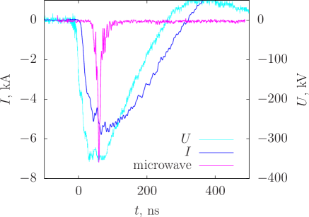
The photonic BWO is studied experimentally using a 350 keV, 5.5 kA, 150 ns electron beam, which is generated by a Marx generator: typical voltage and current pulses are presented in Fig.1. The pencil-like electron beam of 40 mm diameter produced by 35 mm graphite cathode is injected into SWS through the mesh anode, which transparency is 77%. The beam is guided by an axial pulsed magnetic field, which is generated by the discharge of a capacitor bank into a solenoidal coil of 600 mm length. The magnetic field pulse has amplitude about 1 T and duration of several milliseconds at half height. A synchronization circuit ensures generation of the electron beam at the maximal peak value of magnetic field.
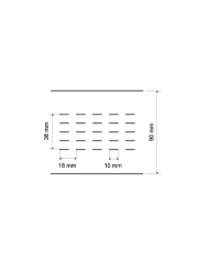
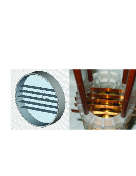
The beam interacts with the foil photonic crystal, which is formed by brass foils strained in the cross-section of cylindrical waveguide with inner diameter 90 mm. Foils’ width and thickness are 10 mm and 250 m, respectively. The crystal comprises 10 periods, each period has 5 foils in cross-section (see Fig. 2).
A waveguide reflector is placed behind the anode to enable reflection of the backward wave towards the output window. The waveguide reflector consists of 4 periods of corrugated waveguide. The inner diameter of the straight circular corrugated waveguide is 50 mm, corrugation period, width and depth are 29 mm, 8 mm and 5 mm, respectively. Reflectance approaching 100% is provided by this reflector in the range from 0 to 4.7 GHz. The anode mesh enables effective reflection in the rest frequency ranges.
Horn antenna with exit aperture 480 mm is used for radiation output. The strength of electric field is detected at the distance 5 m by a receiving antenna and passed by the coaxial cable of RG 402 type to the input of digital oscilloscope Tektronix TDS7404. The detected time-domain waveforms are analyzed using short-time Fourier transform to evaluate spectral content.
III Dispersion characteristics of foil photonic crystal
Electromagnetic waves generation by an electron beam moving in a photonic crystal can be analyzed using the dispersion equation, which defines the relation between frequency and photon wave number in the crystal. The analytic solution of Maxwell equations for the photonic crystal of the considered geometry cannot be found, thus the dispersion properties of the crystal are analyzed numerically as it was done in [3].
Dispersion curves for the low-order modes existing in the above described photonic crystal are shown in Fig. 3. The light line and the beam lines for electron beam energies 200 and 350 keV are also shown. Intersections of dispersion curves and beam lines correspond to the points, where Cherenkov synchronism is achieved [15, 16].
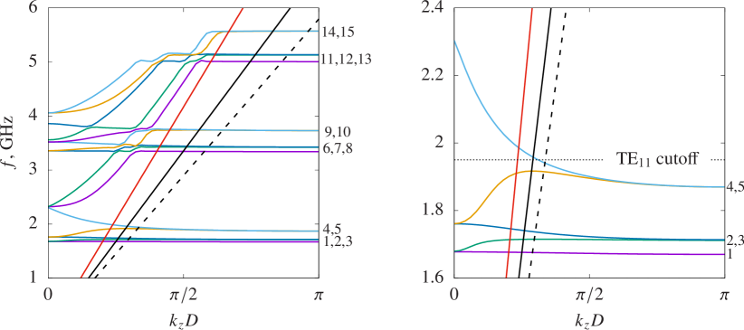
Note that for some of modes shown in Fig. 3, the waves group velocity in these points is negative (i.e. is directed backward the beam velocity). Such modes are classified in [14] as negative dispersion ones. Frequencies for these modes are below cutoff for the regular cylindrical waveguide with the same inner diameter: for a waveguide with internal diameter 90 mm the cutoff frequency for azimuthally symmetric mode TM01 and for nonsymmetric mode TE11 are 2.55 and 1.95 GHz, respectively.
The considered photonic crystal is not axially symmetric. Therefore, one cannot establish a strict correspondence between the types of electromagnetic waves, which are excited inside it, and the eigenmodes of the regular cylindrical waveguide. Structure of modes excited inside the foil photonic crystal for values enabling Cherenkov synchronism is presented in Fig. 4; mode numbering starts from the lowest mode, the mode structure patterns are respectively numbered. Field energy is mainly concentrated inside the crystal in between the foils that makes these modes quite different from the eigenmodes of the regular cylindrical waveguide.
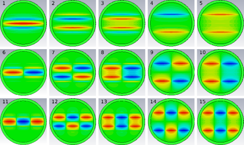
The mode structure patterns (see Fig. 4) for modes numbered 1,3,5,11 and 13 are symmetric with respect to vertical and/or horizontal planes, while for modes 2,4,6,7,8,9,10,12,14 the axial E-field component is distributed antisymmetric and at the waveguide axis. Therefore, the electron beam passing through the photonic crystal along the waveguide axis gets into minima for antisymmetric modes and beam-wave interaction for the them is suppressed as compared with symmetric those. As a result, generation at 1.5 - 2.0 GHz and 5 GHz is expected to be observed.
IV Experimental results
In experiments at electron beam energy 200 keV, which are described in paper [3], generation at below cutoff frequencies was observed, however, single frequency generation was not obtained. In major part of shots the most of radiated power density was concentrated in 5.2 GHz (see Fig. 5) i.e. in 11-th and 13-th modes, which structure is shown in Fig. 4.
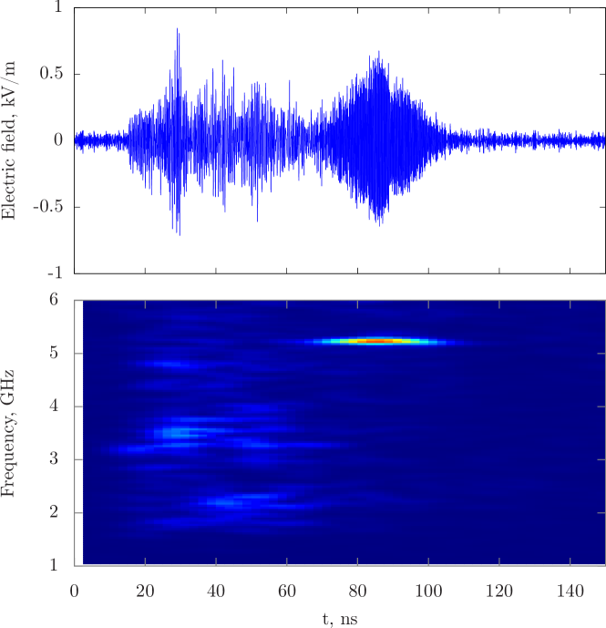
Cherenkov synchronism condition for these modes was fulfilled at value approaching , enabling these modes to be effectively excited by the 200-keV beam [3, 6]. Symmetric mode structure enabled effective interaction with electron beam over its whole cross-section. In some shots generation at below cutoff frequencies was excited at rising diode current (Fig. 6). While generation for antisymmetric modes is significantly suppressed that is in full accordance with the above analysis.
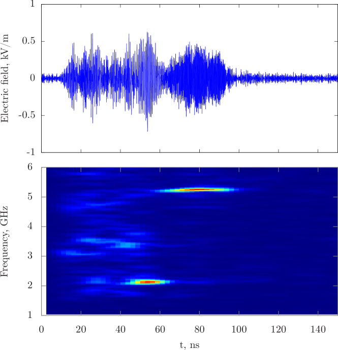
The following reasoning justifies increase of electron beam energy with the goal to observe single-frequency generation at below cutoff modes. According to Fig. 3 growth of the electron beam energy shifts Cherenkov synchronism away from the -point for modes 11 and 13, thus excitation of these modes at electron beam energy 350 keV is expected to be suppressed. Modes 1, 3 and 5 would contribute to radiated power in 1.5–2.0 GHz.
Example of experimentally observed at electron beam energy 350 keV radiated waveform and their spectral content is shown in Fig. 7. Generation at 11-th and 13-th modes is strongly suppressed (absent) in this experiment. In Fig. 7 the most of radiated power density is observed at 1.550.05 GHz, which is below cutoff.
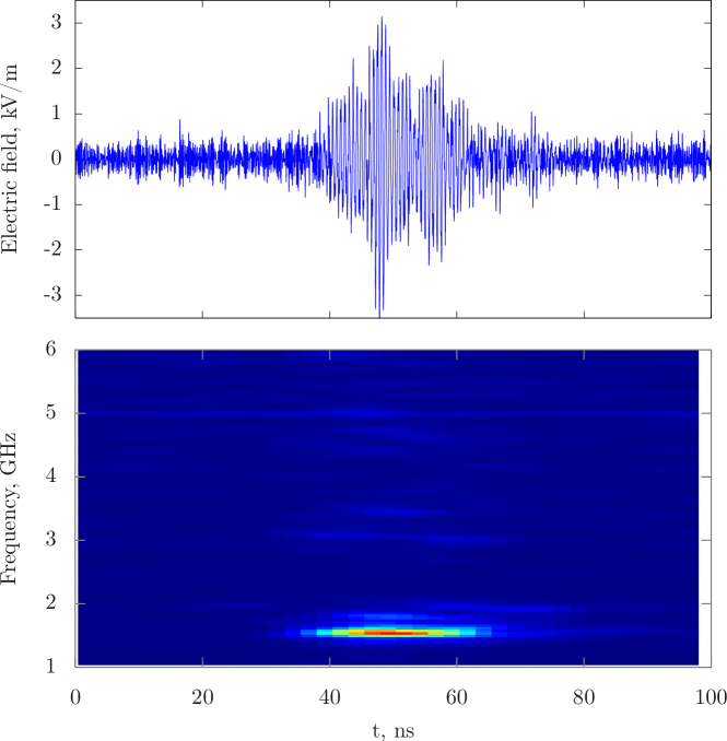
Generation at this frequency can be associated with excitation of the 1-st and/or the 3-rd modes (Fig. 3). The detected frequency 1.55 GHz is a little bit lower than that (1.67 GHz) obtained from the analysis of dispersive curves for the photonic crystal in the circular waveguide in the absence of electron beam. This difference can be specified by influence of electron beam space charge.
V Conclusion
Single frequency generation at the below cutoff modes in the photonic BWO, which uses foil photonic crystal for high power microwave generation, is demonstrated. Excitation of either single the lowest mode or several closely spaced lower modes results in single frequency generation.
References
- [1] Baryshevsky V.G., Spontaneous and induced radiation by electrons/positrons in natural and photonic crystals. Volume free electron lasers (VFELs): From microwave and optical to X-ray range, NIM B355 (2015) pp. 17-23. DOI: 10.1016/j.nimb.2015.04.004
- [2] V.G. Baryshevsky, A.A. Gurinovich, Spontaneous and induced parametric and Smith-Purcell radiation from electrons moving in a photonic crystal built from the metallic threads, NIM B252, No.1 (2006), pp.92-101, DOI:10.1016/j.nimb.2006.07.009.
- [3] Vladimir G. Baryshevsky, Nikolai A. Belous, Alexandra A. Gurinovich, Evgeni A. Gurnevich, Viktor A. Evdokimov and Pavel V. Molchanov, Experimental studies of volume FELs with a photonic crystal made of foils, Proc. of the 32st Intern. Free Electron Laser Conference FEL2010 (2010), p.632-635.
- [4] Vladimir G. Baryshevsky, Nikolai A. Belous, Alexandra A. Gurinovich, Evgeni A. Gurnevich, Viktor A. Evdokimov, Pavel V. Molchanov, Experimental studies of Volume FELs with a photonic crystal, Proc. of 35th International Conference on Infrared, Millimeter, and Terahertz Waves, DOI: 10.1109/ICIMW.2010.5612862
- [5] V.G.Baryshevsky, P.V. Molchanov, Volume Free Electron Laser with a ”Grid” Photonic Crystal in a Cylindrical Waveguide, Acta Physica Polonica A, 115 (2009) pp.971-972, DOI: 10.12693/APhysPolA.115.971.
- [6] V. Baryshevsky, N. Belous, A. Gurinovich, E. Gurnevich, V. Evdokimov, P. Molchanov, Volume Free Electron Laser with a ”Grid” Photonic Crystal with Variable Period: Theory and Experiment, FEL2009, Liverpool, August 2009, MOPC49, p.134-137.
- [7] M. A. Shapiro, S. Trendafilov, Y. Urzhumov, A. Alu, R. J. Temkin and G. Shvets, Active negative-index metamaterial powered by an electron beam, Phys. Rev. B 86 (2012) 085132, DOI: 10.1103/PhysRevB.86.085132.
- [8] Jason Samuel Hummelt, Samantha M. Lewis, Michael A. Shapiro and Richard J. Temkin, Design of a Metamaterial-Based Backward-Wave Oscillator, IEEE Trans. on Plasma Sci. 42, No.4 (2014) pp. 930-936, DOI: 10.1109/TPS.2014.2309597.
- [9] Yanshuai Wang, Zhaoyun Duan, Fei Wang, Shifeng Li, Yan Nie, Yubin Gong, Jinjun Feng, S-band high-efficiency metamaterial microwave source, IEEE Trans. on Elecron Devices 63 , No. 9 (2016) pp. 3747 - 3752, DOI:10.1109/TED.2016.2593701.
- [10] Don Shiffler, John Luginsland, David M. French, and Jack Watrous, A Cerenkov-like Maser Based on a Metamaterial Structure, IEEE Trans. on Plasma Sci. 38, No. 6, (2010) pp.1462 - 1465, DOI: 10.1109/TPS.2010.2046914 .
- [11] Sabahattin C. Yurt, Mikhail I. Fuks, Sarita Prasad, and Edl Schamiloglu, Design of a metamaterial slow wave structure for an O-type high power microwave generator, Physics of Plasma 23, (2016) 123115, DOI: 10.1063/1.4972535.
- [12] Yanshuai Wang, Zhaoyun Duan, Xianfeng Tang, Zhanliang Wang, Yabin Zhang, Jinjun Feng, and Yubin Gong, All-metal metamaterial slow-wave structure for high-power sources with high efficiency, Appl. Phys. Lett. 107, 153502 (2015), DOI: 10.1063/1.4933106.
- [13] I. S. Nefedov, X. Dardenne, C. Craeye, and S. A. Tretyakov, Backward waves in a waveguide filled with wire media, Microw. Opt. Technol. Lett. 48, No.12 (2006) pp.2560-2564, DOI:10.1002/mop.21999.
- [14] S. C. Yurt, A. Elfrgani, M. I. Fuks, K. Ilyenko and E. Schamiloglu, Similarity of Properties of Metamaterial Slow-Wave Structures and Metallic Periodic Structures, IEEE Trans. on Plasma Sci. 44, No.8 (2016) pp. 1280-1286, DOI:10.1109/TPS.2016.2535305.
- [15] V.L. Granatstein, I. Alexeff, High Power Microwave Sources, Boston, MA: Artech House, 1987.
- [16] J. Benford, J.A. Swegle, and E. Schamiloglu, High Power Microwaves, Second Edition, CRC Press, 2007.