Topological phases in the compound
Abstract
Based on first-principles calculations, we show that stoichiometric TaSe3, synthesized in space group , belongs to a three-dimensional (3D) strong topological insulator (TI) phase with invariants (1;100). The calculated surface spectrum shows clearly a single Dirac cone on surfaces, with helical spin texture at a constant energy contour. To check the stability of the topological phase, strain effects have been systematically investigated, showing that many topological phases survive in a wide range of the strains along both the a- and c-axes, such as strong TI (STI), weak TI (WTI) and Dirac semimetal phases. TaSe3 provides us an ideal platform for experimental study of topological phase transitions. More interestingly, since superconductivity in TaSe3 has been reported for a long time, the co-existence of topological phases and superconducting phase suggests that TaSe3 is a realistic system to study the interplay between topological and superconducting phases in the future.
pacs:
03.67.Mn, 05.30.Pr, 73.43.-fI introduction
The layered transition-metal trichalcogenides MX3 (M=Nb, Ta; X=S, Se) have attracted lots of interest because of the appearance of the charge-density-wave (CDW) states at low temperature (LT)Tsutsumi et al. (1977); Wilson (1979); Cava et al. (1985); Srivastava and Avasthi (1992). For instance, both TaS3Cava et al. (1985) and NbSe3Ekino and Akimitsu (1987) are metals at room temperature (RT), and undergo two different CDW transitions as decreasing temperature. But TaSe3 is an exception, in which no CDW transition has been found yetHaen et al. (1978). Instead, TaSe3 remains semimetallic from RT to LT and becomes superconducting at T K Sambongi et al. (1977); Yamamoto (1978); Nagata et al. (1989). The earlier theoretical studiesCanadell et al. (1990) suggest that it could be either a semiconductor or a semimetal, depending on the relative energy level of an anti-bonding Se band to that of the Ta band. So far, first-principles calculations of TaSe3 have not been reported yet, and the electronic structures, Fermi surfaces and topological properties are still unrevealed.
Meanwhile, topological superconductors have attracted much interest due to the emergence of Majorana fermionsWilczek (2009); Leijnse and Flensberg (2012) and the potential application in quantum computationKitaev (2003). The previous work by Fu et al.Fu and Kane (2008) has proposed that the topological superconductivity can be realized on the interface between a TI and a BCS superconductor by proximity effectYan et al. (2013); Wang et al. (2015); Wu et al. (2015); Schoop et al. (2015); Xu et al. (2016). Very recently, topological superconductivity has been observed on the surface of iron-based superconductors below TcZhang et al. (2017), which suggests that a more promising approach to engineer TSCs is to propose superconducting materials with non-trivial topology in their electronic structuresWang et al. (2015). Herein, this approach would avoid the structural compatibility and overcome the fabrication challenges related to the interfaces or heterostructuresWu et al. (2015); Wang et al. (2015); Schoop et al. (2015); Xu et al. (2015); Xing et al. (2016); Xu et al. (2016); Wang et al. (2016). However, most superconductors do not have non-trivial bulk topology in electronic structuresDas et al. (2012); Yan et al. (2013), and some topological candidates do need doping to induce superconductivity, like CuxBi2Se3Hor et al. (2010); Wray et al. (2010), FeTexSe1-xWang et al. (2015); Zhang et al. (2017), etc. Therefore, it is challenging to find a superconductor with non-trivial electronic topology.
In this work, based on first-principles calculations, we show that the single crystal , known as a superconductor for many yearsSambongi et al. (1977); Yamamoto (1978); Nagata et al. (1989), has non-trivial electronic structure. The crucial band inversion happens at B point even without spin-orbit coupling (SOC). This is different from the situation in Bi2Se3Zhang et al. (2009, 2010), in which the band inversion is due to the strong SOC effect. Our detailed analysis indicates that the band inversion is attributed to the “broken” type II chains, especially the Se3-Ta1 and Se6-Ta2 bonds. To shorten these bonds by compressive strains would enlarge the band gap and remove the band inversion. Inclusion of SOC in TaSe3 opens a continuous direct gap in the entire Brillouin zone (BZ), but doesn’t change the energy ordering of the bands at the time-reversal invariant momentum (TRIM) points. The invariants (;,,)Hasan and Kane (2010); Qi and Zhang (2011) are calculated to be (1;100). The strong topological index guarantees the existence of the Dirac-cone states on surfacesFu et al. (2007), which has been further confirmed by our surface calculations. To check the stability of the topological phase, strain effects have been systematically investigated, showing that many topological phases survive in a wide range of the strains along both the - and -axes, such as STI, WTI and Dirac semimetal phases. It’s an ideal platform for experimental study of topological phase transitions. As it becomes superconducting below Tc, TaSe3 also provides us a realistic system to investigate the interplay between the topological surface states and superconductivity.
This paper is organized as follows. In Sec. II we will introduce the details of first-principles calculations. In Sec. III, the calculation results are presented. Finally, Sec. IV contains the discussion and conclusion.
II calculation method
The first-principles calculations were performed within the framework of full-potential linearized-augmented plane-wave (FP-LAPW) method implemented in WIEN2K simulation packageBlaha et al. . Modified Becke-Johnson exchange potential together with local density approximation for the correlation potential was used to obtain accurate band structuresTran and Blaha (2009). SOC was included as a second variational step self-consistently. The radii of the muffin-tin sphere (RMT) were 2.5 Bohr for Ta and 2.38 Bohr for Se, respectively. The -points sampling grid of the BZ in the self-consistent process was 7 19 6. The truncation of the modulus of the reciprocal lattice vector , which was used for the expansion of the wave functions in the interstitial region, was set to . The geometry optimization including SOC interaction was carried out within the framework of the projector augmented wave (PAW) pseudopotential method implemented in Vienna simulation package (VASP)Kresse and Furthmüller (1996a, b). The ionic positions were relaxed until force on each ion was less than 0.005 eV . PHONOPY was employed to calculate the phonon dispersion through the DFPT method Togo et al. (2008).
III results
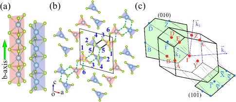
crystallizes in the monoclinic layered structure with space group . The basic building blocks of are parallel trigonal-prismatic chains along the -axis, as shown in Fig. 1(a). Each chain is made by a linear stacking of irregular prismatic cages, which consists of six selenium atoms at the corners and one tantalum atom at the center. In the top view of Fig. 1(b), these chains are classified as type I (i.e., =2.57Å) and type II (i.e., =2.9Å), depending on the shortest bond () of an irregular triangle which is formed by three Se atoms. has two type I and two type II chains in a unit cell. The two chains of each type are related by inversion symmetry. The four prismatic chains have strong bonds (i.e., Se5-Ta1-Se3 and Se5-Ta2-Se6) along the direction, forming the TaSe3 layers as depicted by green dashed lines. The interlayer hoppings are relatively weak compared with the intralayer hoppings, suggesting 2D can be easily produced by exfoliation methods.
Next, we discuss the qualitative electronic structure of by way of a simple Zintl-Klemm conceptNesper (2014). In the type I chain of TaSe3, where the distance between two Se atoms is short enough (i.e., =2.575 Å), a strong covalent - bond is formed. Thus, the oxidation state of the Se3 triangle is (). That’s why ZrSe3 is a semiconductor with Zr4+ and only type I chainsIsland et al. (2017). However, in the type II chain, the distance is not short enough; namely, the - bond is broken. These Se atoms exhibit the normal oxidation states (3Se2-). At the ionic limit, the chemical valence of tantalum is about 5+ (). Thus, (TaSe3)4 can be formulated as 2(4++2) in a primitive unit cell. According to this electron counting model, TaSe3 would be a semiconductor. However, is metallic according to the transport measurementsBuhrman et al. (1980); Bjerkelund et al. (1966), which implies band inversion may occur in the electronic band structure. In order to fully understand the semimetallic propertes of TaSe3, the first-principles calculations have been performed systematically.
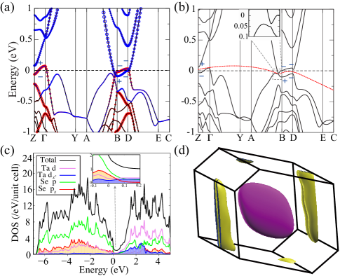
When SOC is ignored, the calculated band structure along high symmetric lines in the BZ is shown in Fig. 2(a). There is always a direct gap between the conduction bands and valence bands, except two crossing points on the AB and DE lines. To elucidate the mechanism of the band inversion, we have calculated the projected weights on six nonequivalent Se atoms (i.e., , and Se6, as shown in Fig. 1(b)) and two nonequivalent Ta atoms (i.e., and , as shown in Fig. 1(b)), respectively. In the fatted-band plot of Fig. 2(a), we denote the weights of Se3 orbital () and Ta1 orbital by the size of the red and blue circles, respectively. We can clearly see that the band and the band have an overlap at the Fermi level (). Further calculated results indicate that the up-going band mainly comes from the states of both Ta1 and Ta2, consistent with the ligand crystal splitting of five orbitals in a prismatic cage. However, the down-going band is mostly from the orbitals of Se3 and Se6 atoms (both of them belong to the “broken” type II chains). To some extent, it suggests that the metallic band structure has to do with the type II chains. These similar results are also obtained by our calculated partial density of states (PDOS) in Fig. 2(c), which show that the Se states and Ta states are mainly located below and above the , respectively, with the hybridization between them. Near , the states are dominated by states of Se3 and Se6 atoms and states of Ta1 and Ta2 atoms.
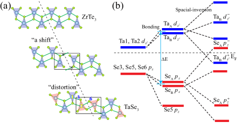
To fully understand the metallic electronic band structure, we first investigate the crystal structure evolution beginning with the layered structure of ZrSe3. In ZrSe3 type I chains are arranged, as shown in Fig. 3(a), as a perfectly layered structure. It can be changed to the crystal structure of TaSe3 by the following two steps. First, a shift may occur along the -direction for every four prismatic chains (MX3)4, as shown in Fig. 3(a). As such, the bonds between selenium and tantalum atoms crossing the black dashed line are broken, as depicted by the symbol “x” in Fig. 3(a). Second, the distortion can happen in the prisms of the box by breaking the shortest - bonds between Se atoms. In addition, the new bonds between Ta2 and Se6 are built. Together, one can find that the crystal environment of Se3 and Se6 atoms of type II chains can change dramatically.
The band inversion can be understood from the bonds (green dashed lines) of Se5-Ta1-Se3 and Se5-Ta2-Se6, which support the layered structure of TaSe3 (see Fig. 1(b) and Fig. 3(a)). In the atomic limit, the energy levels of the Ta orbitals are higher than Se orbitals. Under the crystal field of the prismatic cage, the orbitals are lower than other orbitals. The orbitals of Se atom are higher than other orbitals, since it doesn’t orient toward the Ta atoms. Therefore, only orbitals of Se3, Se5 and Se6, and orbitals of Ta1 and Ta2 are considered in the schematic diagram of the band inversion, as shown in Fig. 3(b). Starting from the atomic limit, the energy level of the Ta orbitals is higher than that of the Se orbitals. In step I, because Se5 forms two bonds while Se3 (or Se6) forms only one bond, the state of Se5 is pushed much lower than the state of Se (or Se). The hybridization makes the two orbitals of Se3 and Se6 form two mixed states, called SeA and SeB, respectively. Similarly, the two mixed states of Ta orbitals are called TaA and TaB. The energy levels are illustrated in the middle of Fig. 3(b). In step II, the inversion symmetry is taken into consideration. Each state can split into two hybridized states, one bonding state and one antibonding state, according to the parity. The band inversion in TaSe3 happens between the bonding state of TaB and antibonding state of SeA, which is consistent with our fatted band calculations and PDOS. This band inversion mechanism is further confirmed by the phase diagram under strains, as will be shown later.
The inclusion of SOC leads to gap opening at the band crossing points, as seen in the band structure of Fig. 2(b). However, the maximum of the valence bands is still higher than the minimum of the conduction bands, which gives rise to the semimetallic properties of TaSe3. The calculated Fermi surfaces consist of a large hole pocket enclosing point and two electron pockets near B point, as shown in Fig. 2(d). Further parity analysis indicates that the inverted two bands have different parity eigenvalues at B point, while they have the same eigenvalue (i.e., ) at D point. Note that the band inversion has already happened even without SOC. The band inversion is attributed to the unique structure of the type II chains, especially the Se3-Ta1 and Se6-Ta2 bonds, which is distinct from the SOC-induced band inversion of the well-known Bi2Se3 family.
To classify TIs, one needs to compute four topological indices , where is a strong topological index and are three weak topological indices. Since there is a continuous direct SOC gap, the Fu-Kane invariants are well defined for the occupied bands below the gap in TaSe3. Due to the existence of inversion center in , they can be easily calculated by Fu-Kane parity criterionFu et al. (2007) at eight TRIM points (). The strong topological index is given by , where is the product of parity eigenvalues of the bands at without counting their time reversal partners. Three weak topological indices are defined at the four TRIM points in a plane offset from point. Explicitly, , and . The space group of is non-symmorphic with a screw symmetry , which is a twofold rotation about the -axis followed by a half lattice translation in the same direction (). It satisfies the relation , where is inversion symmetry and the lattice translation can be represented by a phase factor in the Bloch basis: . Thus, at the TRIM points in the plane, i.e., A, C, E and Y, with the expression , anticommutates with . In combination of time reversal symmetry, the anticommutating relation leads that all the states are four-fold degenerate, consisting of two parity bands and two parity bands (i.e., “”). Considering that the total number of valence bands is , we get =====. Therefore, the strong topological index is determined by band inversion at other four TRIMs (Z, , B and D). Their parity products are calculated to be === and =, which are extracted from standard numerical calculations based on first-principles calculations. Therefore, the topological invariants of turn out to be (1;100).
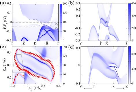
In view of the fact that the hallmark of topological non-trivial property is the existence of topological non-trivial surface states, the tight-binding Hamiltonians of semi-infinite samples are constructed by the maximally localized Wannier functions (MLWFs) for all the Ta and Se orbitals, which are generated from the first-principles calculations. The surface Green’s functions of the semi-infinite sample are obtained using an iterative methodMarzari et al. (2012). The local DOS (LDOS), extracted from the imaginary part of the surface Green’s function, is used to analyze the surface band structures. For STIs, the existence of an odd number of Dirac cones on the surface is ensured by the strong topological index =1. On the (010) surface of TaSe3, a Dirac cone is obtained at point in Fig. 4(a), which hosts helical spin texture at the energy contour (E=EF) in Fig. 4(c). On the (10) surface, a Dirac cone is found at point, as shown in Fig. 4(b) and its zoom-in plot in Fig. 4(d). The existence of a single Dirac cone on the surfaces is consistent with the STI phase.

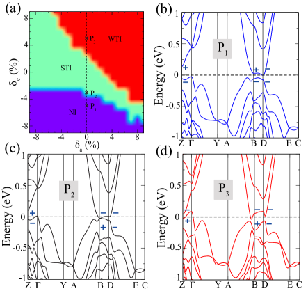
Since it’s a layered structure with trigonal-prismatic chains going in the -direction, the lattice parameters in - and -directions are supposed to be more sensitive to temperature or strain than that in the -direction. Therefore, the strain effects along the - and -directions have been systematically investigated in our calculations, in order to check the stability of the STI phase. For each given lattice constant, the internal positions of the atoms are fully relaxed until the force on each atom satisfies the required precision. The computed phase diagram is shown in Fig. 5(a) as a function of lattice parameters (horizontal axis) and (vertical axis). On the vertical dashed line in Fig. 5(a) (i.e., the strain in the -direction is zero), when grows from to (with the lattice parameter without strain), it changes from a normal insulating (NI) phase, to STI phase, and then to WTI phase due to band inversion happening at TRIMs successively. Explicitly, at the beginning (), no band inversion is found in Fig. 5(b) and the system is a trivial insulator. When , two bands of opposite parity become touching at B point, as shown in Fig. 5(c), resulting in a Dirac semimetal phase at the phase transition point. After the transition point, the system enters STI phase. By increasing further (e.g. ), another band inversion occurs at Z point, the system turns to WTI phase, as shown in Fig. 5(d). As we can see in Fig. 5(a), both STI (green) and WTI (red) phases survive in a considerable region compared with the NI (blue) phase. The phase boundaries are Dirac semimetals, which may also be observed in experiments. The phase diagram provides us an important roadmap to regulate the topological phase transitions in . Compared with the reported topological materials, TaSe3 has two unique features. First, the compressive strain can remove the band inversion, which is different from the common concept that the compressive strain usually enhances the band inversionNie et al. (2015a); Sisakht et al. (2016); Shao et al. (2017). The compressive strain shortens the distances of the bonds of Ta1-Se3 and Ta2-Se6, the hybridization becomes stronger and the average gap is enlarged between SeA (SeB ) and TaA (TaB ) states. Second, many TIs have an -type band inversion or a -type band inversion Nie et al. (2015a); Sisakht et al. (2016); Shao et al. (2017), while TaSe3 has a -type band inversion. Third, most TIs only have band inversion at one TRIM point (such as the point)Zhang et al. (2010); Nie et al. (2015b), while TaSe3 has band inversion at three TRIM points, which leads to fruitful nontrivial phases under different strains, including 3D STI, 3D WTI and Dirac semimetal.
Next, we would like to discuss the possible CDW in TaSe3. It is well-known that no CDW is observed in NbS2. However, the phonon dispersion shows imaginary frequencies based on first-principles calculations Heil et al. (2017). In order to exclude the possibility of the latent CDW instability and greatly support our predictions of nontrivial topological properties in TaSe3, we carefully calculate the phonon dispersion for TaSe3, which is shown in Fig. 6(a). No imaginary frequency is found in the dispersion. The phonon calculations have also been checked with respect to many parameters, such as -point grid, type of smearing and size of supercell etc. In addition, we also calculate the phonon dispersion of TaSe3 with c=0.95c0 (P1), c=0.97c0 (P2) and c=1.05c0 (P3), as shown in Fig. 6(b), 6(c) and 6(d), respectively. No imaginary frequency can be found in any of them. Therefore, it is safe to exclude the effect of CDW in TaSe3.
IV DISCUSSION and Conclusion
To achieve topological superconductivity, it is challenging to find a material with both nontrivial topology of the electronic structure and superconductivity. A prior theoretical proposal of intrinsic non-trivial material is high-Tc superconductor FeTexSe1-x Wang et al. (2015) with supporting topological surface states at . Very recently, the topological superconducting phase has been verified on (001) surface by spin-resolved ARPES experiments Zhang et al. (2017). Here we show another promising candidate TaSe3, whose superconductivity has been reported for many yearsSambongi et al. (1977); Yamamoto (1978); Nagata et al. (1989), is topologically non-trivial and has spin-momentum locking states on the surface. Compared to the FeTexSe1-x system, TaSe3 does not require doping to introduce superconductivity, implying this superconductor can be grown in high-quality single crystals. At the Fermi level (), as we show in Fig. 4(c), the surface states are well separated from the bulk states. Based on Fu-Kane’s proposal, the superconducting states of the surface states induced by the bulk superconductivity below Tc=2.3 K can be topologically nontrivial. However, if the chemical potential lies 40 meV () below the Fermi level in Fig. 4(a), the surface states merge into the bulk states, which could kill the topological superconducting state and make the surface topological superconducting state sensitive to the position of the chemical potential. The future experimental work is needed to search for the potential topological superconductivity in the system.
In conclusion, we have calculated the electronic structure, and topological properties of with crystal structure by using density functional theory. The calculated topological invariants are (1;100), which indicate that it belongs to the STI phase. A single Dirac cone is obtained in the calculated surface spectra. Further systematical calculations of strain effects suggest can realize multiple topological non-trivial phases under strains, including STI, WTI and Dirac semimetal phases. These topological non-trivial phases survive in a wide range of the strain along the - and -axes, making an attractive platform to study the topological phase transitions. In addition, the co-existence of the topological phases and superconductivity of suggests that it could be a realistic system to study the interplay between topological and superconducting phases in the future.
Acknowledgements.
We thank Prof. Robert J. Cava for useful discussions. F. B. P. and S. N. were supported by Stanford Energy 3.0. W. X. was supported by LSU-startup funding and the Louisiana Board of Regents Research Competitiveness Subprogram (RCS) under Contract Number LEQSF (2017-20)-RD-A-08. Z. W. was supported by the Department of Energy Grant No. DE-SC0016239, the National Science Foundation EAGER Grant No. NOA-AWD1004957, Simons Investigator Grants No. ONR-N00014-14-1-0330, No. ARO MURI W911NF-12-1-0461, and No. NSF-MRSEC DMR- 1420541, the Packard Foundation, the Schmidt Fund for Innovative Research, and the National Natural Science Foundation of China (No. 11504117). L.X. and R.J. are supported by Department of Energy Grant No. SC00i6315.References
- Tsutsumi et al. (1977) K. Tsutsumi, T. Takagaki, M. Yamamoto, Y. Shiozaki, M. Ido, T. Sambongi, K. Yamaya, and Y. Abe, Physical Review Letters 39, 1675 (1977).
- Wilson (1979) J. Wilson, Physical Review B 19, 6456 (1979).
- Cava et al. (1985) R. J. Cava, R. Fleming, R. Dunn, and E. Rietman, Physical Review B 31, 8325 (1985).
- Srivastava and Avasthi (1992) S. Srivastava and B. Avasthi, Journal of materials science 27, 3693 (1992).
- Ekino and Akimitsu (1987) T. Ekino and J. Akimitsu, Japanese Journal of Applied Physics 26, 625 (1987).
- Haen et al. (1978) P. Haen, F. Lapierre, P. Monceau, M. N. Regueiro, and J. Richard, Solid State Communications 26, 725 (1978).
- Sambongi et al. (1977) T. Sambongi, M. Yamamoto, K. Tsutsumi, Y. Shiozaki, K. Yamaya, and Y. Abe, Journal of the Physical Society of Japan 42, 1421 (1977).
- Yamamoto (1978) M. Yamamoto, Journal of the Physical Society of Japan 45, 431 (1978).
- Nagata et al. (1989) S. Nagata, H. Kutsuzawa, S. Ebisu, H. Yamamura, and S. Taniguchi, Journal of Physics and Chemistry of Solids 50, 703 (1989).
- Canadell et al. (1990) E. Canadell, I. Rachidi, J. Pouget, P. Gressier, A. Meerschaut, J. Rouxel, D. Jung, M. Evain, and M. Whangbo, Inorganic Chemistry 29, 1401 (1990).
- Wilczek (2009) F. Wilczek, Nature Physics 5, 614 (2009).
- Leijnse and Flensberg (2012) M. Leijnse and K. Flensberg, Semiconductor Science and Technology 27, 124003 (2012).
- Kitaev (2003) A. Y. Kitaev, Annals of Physics 303, 2 (2003).
- Fu and Kane (2008) L. Fu and C. L. Kane, Physical review letters 100, 096407 (2008).
- Yan et al. (2013) B. Yan, M. Jansen, and C. Felser, Nature Physics 9, 709 (2013).
- Wang et al. (2015) Z. Wang, P. Zhang, G. Xu, L. Zeng, H. Miao, X. Xu, T. Qian, H. Weng, P. Richard, A. Fedorov, et al., Physical Review B 92, 115119 (2015).
- Wu et al. (2015) X. Wu, S. Qin, Y. Liang, C. Le, H. Fan, and J. Hu, Physical Review B 91, 081111 (2015).
- Schoop et al. (2015) L. M. Schoop, L. S. Xie, R. Chen, Q. D. Gibson, S. H. Lapidus, I. Kimchi, M. Hirschberger, N. Haldolaarachchige, M. N. Ali, C. A. Belvin, et al., Physical Review B 91, 214517 (2015).
- Xu et al. (2016) G. Xu, B. Lian, P. Tang, X.-L. Qi, and S.-C. Zhang, Physical Review Letters 117, 047001 (2016).
- Zhang et al. (2017) P. Zhang, K. Yaji, T. Hashimoto, Y. Ota, T. Kondo, K. Okazaki, Z. Wang, J. Wen, G. Gu, H. Ding, et al., arXiv preprint arXiv:1706.05163 (2017).
- Xu et al. (2015) Q. Xu, Z. Song, S. Nie, H. Weng, Z. Fang, and X. Dai, Physical Review B 92, 205310 (2015).
- Xing et al. (2016) Y. Xing, H. Wang, C.-K. Li, X. Zhang, J. Liu, Y. Zhang, J. Luo, Z. Wang, Y. Wang, L. Ling, et al., npj Quantum Materials 1, 16005 (2016).
- Wang et al. (2016) Y.-Q. Wang, X. Wu, Y.-L. Wang, Y. Shao, T. Lei, J.-O. Wang, S.-Y. Zhu, H. Guo, L.-X. Zhao, G.-F. Chen, et al., Advanced Materials 28, 5013 (2016).
- Das et al. (2012) A. Das, Y. Ronen, Y. Most, Y. Oreg, M. Heiblum, and H. Shtrikman, Nature Physics 8, 887 (2012).
- Hor et al. (2010) Y. S. Hor, A. J. Williams, J. G. Checkelsky, P. Roushan, J. Seo, Q. Xu, H. W. Zandbergen, A. Yazdani, N. Ong, and R. J. Cava, Physical review letters 104, 057001 (2010).
- Wray et al. (2010) L. A. Wray, S.-Y. Xu, Y. Xia, Y. San Hor, D. Qian, A. V. Fedorov, H. Lin, A. Bansil, R. J. Cava, and M. Z. Hasan, Nature Physics 6, 855 (2010).
- Zhang et al. (2009) H. Zhang, C.-X. Liu, X.-L. Qi, X. Dai, Z. Fang, and S.-C. Zhang, Nature physics 5, 438 (2009).
- Zhang et al. (2010) W. Zhang, R. Yu, H.-J. Zhang, X. Dai, and Z. Fang, New Journal of Physics 12, 065013 (2010).
- Hasan and Kane (2010) M. Z. Hasan and C. L. Kane, Reviews of Modern Physics 82, 3045 (2010).
- Qi and Zhang (2011) X.-L. Qi and S.-C. Zhang, Reviews of Modern Physics 83, 1057 (2011).
- Fu et al. (2007) L. Fu, C. L. Kane, and E. J. Mele, Physical Review Letters 98, 106803 (2007).
- (32) P. Blaha, K. Schwarz, G. Madsen, D. Kvasnicka, and J. Luitz, WIEN2k, An Augmented Plane Wave Plus Local Orbitals Program for Calculating Crystal Properties (TU Vienna, Vienna, 2001) .
- Tran and Blaha (2009) F. Tran and P. Blaha, Physical Review Letters 102, 226401 (2009).
- Kresse and Furthmüller (1996a) G. Kresse and J. Furthmüller, Computational Materials Science 6, 15 (1996a).
- Kresse and Furthmüller (1996b) G. Kresse and J. Furthmüller, Physical Review B 54, 11169 (1996b).
- Togo et al. (2008) A. Togo, F. Oba, and I. Tanaka, Physical Review B 78, 134106 (2008).
- Nesper (2014) R. Nesper, Zeitschrift für anorganische und allgemeine Chemie 640, 2639 (2014).
- Island et al. (2017) J. O. Island, A. J. Molina-Mendoza, M. Barawi, R. Biele, E. Flores, J. M. Clamagirand, J. R. Ares, C. Sánchez, H. S. van der Zant, R. D Agosta, et al., 2D Materials 4, 022003 (2017).
- Buhrman et al. (1980) R. Buhrman, C. Bastuscheck, J. Scott, J. Kulick, D. Gubser, T. Francavilla, S. Wolf, and J. Leibowitz, in AIP Conference Proceedings, Vol. 58 (AIP, 1980) pp. 207–215.
- Bjerkelund et al. (1966) E. Bjerkelund, J. Fermor, and A. Kjekshus, Acta Chemica Scandinavica 20, 1836 (1966).
- Marzari et al. (2012) N. Marzari, A. A. Mostofi, J. R. Yates, I. Souza, and D. Vanderbilt, Reviews of Modern Physics 84, 1419 (2012).
- Nie et al. (2015a) Y. Nie, M. Rahman, D. Wang, C. Wang, and G. Guo, Scientific Reports 5, 17980 (2015a).
- Sisakht et al. (2016) E. T. Sisakht, F. Fazileh, M. Zare, M. Zarenia, and F. Peeters, Physical Review B 94, 085417 (2016).
- Shao et al. (2017) D. Shao, J. Ruan, J. Wu, T. Chen, Z. Guo, H. Zhang, J. Sun, L. Sheng, and D. Xing, Physical Review B 96, 075112 (2017).
- Nie et al. (2015b) S.-M. Nie, Z. Song, H. Weng, and Z. Fang, Physical Review B 91, 235434 (2015b).
- Heil et al. (2017) C. Heil, S. Poncé, H. Lambert, M. Schlipf, E. R. Margine, and F. Giustino, Physical review letters 119, 087003 (2017).