Doping-induced persistent spin helix with large spin splitting in monolayer SnSe
Abstract
Finding a new class of materials supporting a long spin lifetime is essential in development of energy-saving spintronics, which is achievable by using a persistent spin helix (PSH) materials. However, for spintronic devices, the PSH states with large spin splitting is required for operation at room temperature. By employing first-principles calculations, we show that the PSH states with large spin splitting are achieved in the SnSe monolayer (ML) functionalized by a substitutional halogen impurity. We find the PSH states in the Fermi level where -space Fermi surface is characterized by the shifted two loops, dominated by out-of-plane spin orientations. We clarify the PSH states in term of an effective Hamiltonian obtained from symmetry consideration. Finally, large spin-orbit strength in the PSH states with a substantially small wavelength are found, rendering that this system is promising for the development of an efficient and high-density scalable spintronic devices operating at room temperatures.
pacs:
Valid PACS appear hereI INTRODUCTION
Recent development of spintronics relies on the new pathway for exploiting carrier spins in semiconductors by utilizing the effect of spin-orbit coupling (SOC)Manchon et al. (2015). When the SOC occurs in a system with sufficiently low crystalline symmetry, an effective magnetic field or known as a spin-orbit field (SOF) is induced, where is the electric field originated from the crystal inversion asymmetry and is the momentum, that leads to spin splitting energy Rashba (1960); Dresselhaus (1955). However, due to momentum-dependent of the SOF, electron scatterings randomize the spins, which induces the fast spin decoherence through the Dyakonov-Perel mechanism Dyakonov and Perel (1972). Accordingly, spin lifetime reduces, which limits the performance of potential spintronic devices, e.g., the spin field effect transistor (SFET)Datta and Das (1990). To overcome this problem, finding a novel structure supporting an extended spin lifetime is an important task, which is achievable by using persistent spin helix (PSH) materialsBernevig et al. (2006); Schliemann (2017); Passmann et al. (2018); Koralek et al. (2009); Walser et al. (2012); Kohda et al. (2012); Sasaki et al. (2014); Absor et al. (2015); Yamaguchi and Ishii (2017); Sao and Tsymbal (2018).
The PSH is established on a system having unidirectional SOF, satisfying SU(2) symmetry Bernevig et al. (2006). Here, a uniform spin textures in the momentum -space is induced, resulting in a robust against spin-independent scattering. Such a PSH condition is achieved, in particular, if the strength of the Rashba and Dresselhauss SOC is equal, as recenly reported experimentally on various (001)-oriented QW such as GaAs/AlGaAs QW Koralek et al. (2009); Walser et al. (2012); Schönhuber et al. (2014) and InGaAs/InAlAs QW Ishihara et al. (2014); Kohda et al. (2012); Sasaki et al. (2014). On the other hand, the PSH state can also be achieved on the (110)-oriented QW where the SOC is purely characterized by the Dreseelhauss effect Bernevig et al. (2006). Here, the SOF is enforced to be parallel with the spins in the unidirectional out-of-plane orientation, which has been experimentally observed on (110)-oriented GaAs/AlGaAs QW Chen et al. (2014). This PSH state was also predicted for a wurtzite ZnO (10-10) surface Absor et al. (2015) and strained LaAlO3/SrTiO3 (001) interface Yamaguchi and Ishii (2017). Although the PSH has been experimentally realized in various QW systems Ishihara et al. (2014); Kohda et al. (2012); Sasaki et al. (2014); Koralek et al. (2009); Walser et al. (2012); Schönhuber et al. (2014), it is practically non-trivial. This is due to the fact that achieving the PSH state requires to control precisely the strength of the Rashba and Dresselhauss SOC, for instant, by tuning the QW width Koralek et al. (2009); Walser et al. (2012) or using an external electric field Ishihara et al. (2014); Kohda et al. (2012); Sasaki et al. (2014).
Since the orientation of the SOF is enforced by the direction of the electric field , the PSH states may appear intrinsically on a material exhibiting internal electric polarization. Here, two-dimensional (2D) ferroelectric materials such as tin monoselenide (SnSe) monolayer (ML) comprises promising candidate for the PSH material since it was predicted to have large in-plane electric polarization Fei et al. (2016); Barraza-Lopez et al. (2018). This electric polarization is expected to induce electric field in the in-plane direction, which imposes the SOF becoming out-of-plane unidirectional Absor et al. (2015). Recently, the SnSe ML has been succsesfully synthesized experimentally using vapor deposition processes Zhang et al. (2014) or the one-pot route Li et al. (2013), which shows high carrier mobility Xu et al. (2017) and anisotropic electrical conductivity Shi and Kioupakis (2015). Therefore, the experimental realization of the SnSe ML as a PSH material is plausible. Although the SnSe ML possibly supports the PSH states, this material posses small spin splitting energy ( meV) Shi and Kioupakis (2015); Gomes and Carvalho (2015), which provides a disadvantage for spintronic devices. Therefore, finding a suitable adjustment method to achieved the large spin splitting in the SnSe ML is a great challenge.
In this work, we proposed to use a halogen doping for inducing large spin splitting in the SnSe ML. Introducing the halogen doping is expected to enhance the in-plane electric polarization through in-plane ferroelectric distortion, which evidently gives rise to the large spin-splitting. In fact, the large spin splitting induced by a halogen doping has been recently reported on various 2D transition metal dichalcogenides (TMDs) such as WSe2 Guo et al. (2017) and PtSe2 MLs Absor et al. (2018a). By employing fully relativistic density-functional theory (DFT) calculations, we find that the PSH state with large spin splitting is achieved on the SnSe ML functionalized by a halogen substitutional doping. We identify the PSH states at Fermi level where the the -space Fermi surface is characterized by the shifted two loops, dominated by the out-of-plane spin textures. We analysed the PSH states in term of an effective Hamiltonian obtained from symmetry consideration. Finally, we estimate the spin splitting-related parameters such as spin-orbit strength and the wavelength of the PSH states, and discuss the possible application in the spintronic devices.
II Computational Details
We performed first-principles electronic structure calculations based on the non-collinear density functional theory (DFT) within the generalized gradient approximation (GGA) Perdew et al. (1996) using the OpenMX code Ozaki et al. (2009). We used norm-conserving pseudopotentials Troullier and Martins (1991), and the wave functions are expanded by the linear combination of multiple pseudoatomic orbitals generated using a confinement scheme Ozaki (2003); Ozaki and Kino (2004). In our DFT calculations, the SOC is included by using -dependent pseudopotentials (Theurich and Hill, 2001). The basis functions of each atoms are two -, two -, two -character numerical pseudo-atomic orbitals.
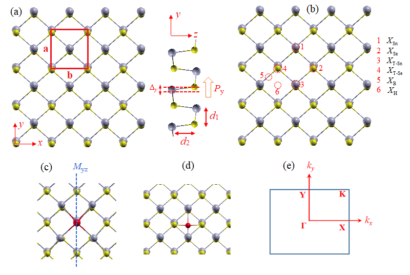
We used a periodic slab to model the SnSe ML, where a sufficiently large vacuum layer (20 Å) is applied to avoid interaction between adjacent layers. The crystal structures of the SnSe ML with ferroelectric phase (Fei et al., 2016) were used. Here, we used the axes system where layers are chosen to sit on the plane, i.e., perpendicular to the direction [Fig. 1(a)]. The axis is taken to be parallel to the puckering direction, which is similar to the system used for black phosphorus Popović et al. (2015). The calculated lattice parameters are Å and Å, which is in a good agreement with previous calculation Gomes et al. (2015, 2016); Xu et al. (2017); Haleoot et al. (2017).
We then introduced a doping with external element taken from the halogen (Cl, Br, and I) atoms. Here, the halogen dopant can either occupy a substitutional position or adsorb on the surface following Boltzmann distribution to form a point defect. In the case of the substitutional doping, we considered and defined as the halogen substitution on the Sn and Se sites, respectively. On the other hand, for the case of the absorption, various halogen doping positions such as top of the Sn atom (), top of the Se atom (), in-plane bridge between the Sn and Se atoms (), and hollow surface () were considered [Fig. 1(b)]. To model these doping systems, we construct a 4x4x1 supercell of the SnSe ML with 64 atoms. The larger supercells (5x5x1 and 6x6x1 supercells) are used to test our calculation results, and we confirmed that it does not affect the main conclusion. The geometries were fully relaxed until the force acting on each atom was less than 1 meV/Å.
To confirmed stability of the doped SnSe, we calculated the formation energy defined as
| (1) |
where and are the total energy of the doped and pristine SnSe ML, respectively. In Eq. (1), is the chemical potentials of constituent , while is the total energy calculated for the most stable element crystal. is the number of the component atoms added to (negative ), or taken from (positif ) the host. There are many thermodynamic limits on the achievable values of the chemical potential under equilibrium growth conditions Wei and Zhang (2002). first, to avoid precipitation of the elemental dopant and the host elements (Sn and Se), are bound by
| (2) |
Second, the sum of the chemical potentials of all component elements should be equal to the host compound:
| (3) |
where is the formation energy of the SnSe ML. In our calculation, we found that eV, which is in a good agreement with previous result obtained by Tang et. al. (Tang et al., 2018a). Finally, to avoid the formation of secondary phases between the halogen dopants and host element, is limited by:
| (4) |
| (5) |
where and are the formation energy of SnSe2 and Sn MLs.
| Cl | Br | I | |||||||
|---|---|---|---|---|---|---|---|---|---|
| Impurity type | Sn-rich (eV) | Se-rich (eV) | Sn-rich (eV) | Se-rich (eV) | Sn-rich (eV) | Se-rich (eV) | |||
| Substitution | |||||||||
| 2.12 | 1.57 | 2.47 | 1.8 | 0.2.74 | 1.91 | ||||
| 0.76 | 0.42 | 0.81 | 0.58 | 0.94 | 0.77 | ||||
| Absorption | |||||||||
| 0.85 | 1.10 | 0.92 | 1.23 | 1.09 | 1.34 | ||||
| 1.2 | 2.01 | 1.55 | 2.43 | 1.91 | 2.78 | ||||
| 1.63 | 2.21 | 1.95 | 2.79 | 2.19 | 2.98 | ||||
| 0.78 | 0.91 | 0.82 | 1.04 | 0.98 | 1.11 | ||||
III RESULT AND DISCUSSION
First, we briefly discuss the structural and electronic properties of the pristine SnSe ML. From symmetry point of view, crystal structure of the SnSe ML is non-centrosymmetric, which is characterized by three non-trivial symmetry operations, namely a vertical mirror plane () parallel to the plane, a two-fold screw rotation along the axes parallel to the direction, and a glide reflection on a plane parallel to the plane. Here, the Sn and Se atoms have an opposing displacement within the plane [Fig. 1(a)], which induces in-plane ferroelectric distortion in the -direction [Fig. 1(b)]. This distortion will generate in-plane electric polarization Fei et al. (2016); Barraza-Lopez et al. (2018), and then induces in-plane electric field , which plays an important role for inducing the PSH states.
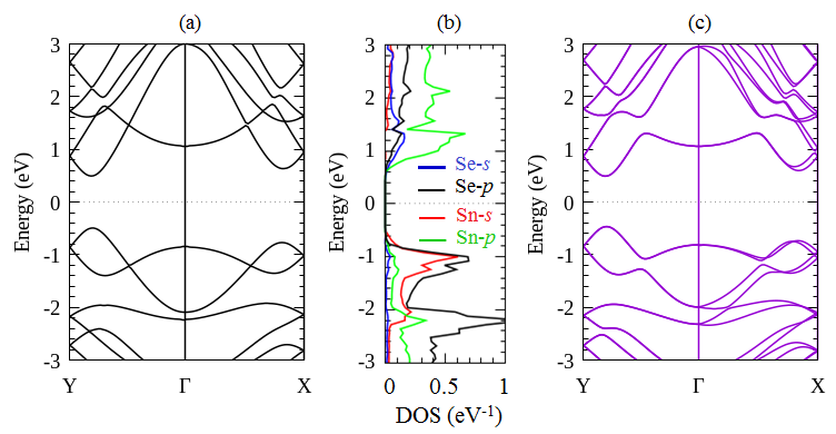
Figure 2(a) shows the calculated result of the electronic band structures of (1x1) unit cell of the SnSe ML. The first Brillouin zone used in our calculations is shown in Fig. 1(e). Consistent with previous result Shi and Kioupakis (2015); Gomes and Carvalho (2015), we find two equivalent band dispersions near the gap, which is located along the and lines [Fig. 2(a)]. However, both the valence band maximum (VBM) and conduction band minimum (CBM) are located on the same point in the line, resulting in the direct gap semiconductor with energy gap of 0.95 eV. Our calculated density of states (DOS) projected to the atom confirmed that the Sn- and Se- orbitals contribute mostly to the VBM, while the CBM is mainly originated from the contribution of the Sn- and Se- orbitals [Fig.2(b)].
Turning the SOC gives rise to the spin-split bands in all the Brillouin zone except for the line [Fig. 2(c)]. The observed spin degeneracy along the line is due to the fact that this line is parallel to the direction of the in-plane electric field in which the mirror symmetry is preserved. Away from the spin-degenerate line, the spn splitting is established. Especially in the CBM along line, the spin splitting energy of 51.6 meV is observed, which is in a good agreement with previous report ( meV) Shi and Kioupakis (2015); Gomes and Carvalho (2015). Because the spin splitting is suppressed by the in-plane electric field , it is expected that the spin directions at each spin-split bands are enforced to be perpendicular (out-of-plane) to the SnSe ML surface, which induces the PSH states. This mechanism for inducing the PSH states is similar to the recently reported PSH states on the (110)-oriented GaAs/AlGaAs QW Chen et al. (2014) and ZnO (10-10) surface Absor et al. (2015).
Next, we consider the effect of the halogen doping on the structural and electronic properties of the SnSe ML. We confirmed the stability of the doped systems (, , , , , and ) by the calculated formation energy shown in Table 1. We find that the and have the lowest under Se-rich and Sn-rich conditions, respectively, indicating that both the systems are the most stable halogen doping formed in the SnSe ML. This is consistent with earlier report that the halogen atom can be easily formed in the group-IV monochalcogenide through substitution on the chalcogen site as found in the bulk SnSe Zhou et al. (2018a), bulk SnS Malone et al. (2014), and GeSe ML (Ao et al., 2015), or by absorption on the hollow site of the surface as found in the GeSe ML Li et al. (2017). On the contrary, the formation of the other dopings (, , , and ) is highly unfavorable due to the required electron energy. This is due to the fact that the present of the halogen doping induces covalent bonding between the Sn and the halogen atoms, which is stabilized by breaking the crystal symmetry, thus increasing the .
| System | (Å) | (Å) | (Å) | (Å) | (Å) | |||||
|---|---|---|---|---|---|---|---|---|---|---|
| Pristine | 2.89 | 2.76 | 0.34 | - | - | |||||
| Substitutional doping | ||||||||||
| Cl | 3.20 | 2.80 | 0.39 | - | - | |||||
| Br | 3.24 | 2.84 | 0.42 | - | - | |||||
| I | 3.37 | 3.09 | 0.44 | - | - | |||||
| Absorption doping | ||||||||||
| Cl | - | - | - | 3.39 | 4.14 | |||||
| Br | - | - | - | 3.42 | 4.21 | |||||
| I | - | - | - | 3.50 | 4.28 |
When the doping is introduced, the relaxation substantially changes the pristine atomic positions. Here, we consider both the and because they have the lowest among the other doping systems. In the case of the , the relaxation suppressed that only mirror symmetry still remains [Fig. 1(c). Since the bondlength between the Sn and halogen atoms in the in-plane () and out-of-plane () directions are much larger than that between the Sn and Se atoms in the pristine system [see Table 2], a significant in-plane distortion is induced. For instant, in the case of the , we find that Å and Å, resulting in that Å. This value is larger than that of the pristine system ( Å), indicating that strong enhancement of the in-plane ferroelectricity is achieved. In contrast, the formation of the results in a square piramidal-like structure [Fig. 1(d)], where the average bondlength between the Sn or Se and halogen atoms ( ,) is substantial [see Table 2]. However, there is no in-plane distortion observed in the , indicating that the dosn’t support the in-plane ferroelectricity. Because the in-plane ferroelectricity plays an important role for inducing the PSH states, in the following discussion we will focus only for the .
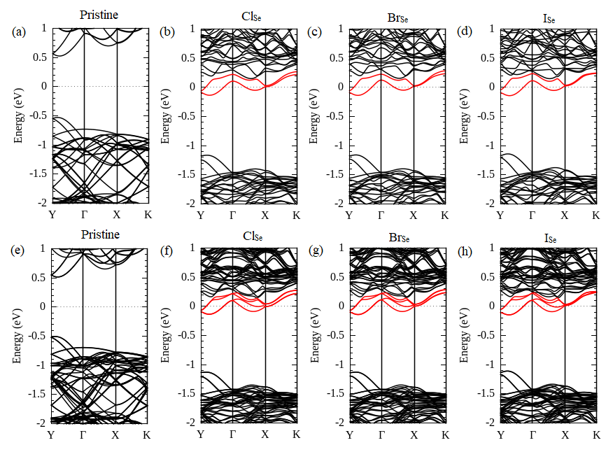
Figure 3 shows the electronic band structures of the doping () systems compared with those of the pristine one. In contrast to the pristine system [Figs. 3(a) and 3(e)], we identify impurity states in the band structures of the , which are located close to the CBM around the Fermi level [Figs. 3(b)-(d)]. This indicates that -type doping is achieved, which is similar to the recent prediction of the -type system on bulk SnS doped by Cl atom (experiment) Yanagi et al. (2016) and bulk SnSe doped by Br and I atoms (theory) Zhou et al. (2018b). More importantly, we find spin-split bands in the impurity states when the SOC is taken into account [Figs. 3(b)-(d)], indicating that this system is promising for spintronics.
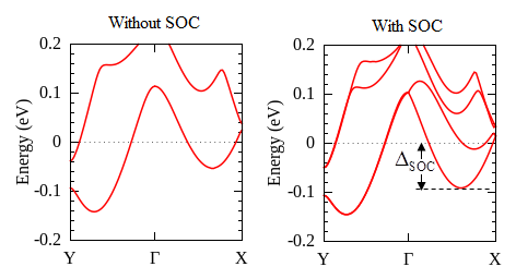
To analyse the properties of the spin-split bands in the impurity states of the , we choose the I as a representative example. Here, we focused on the spin-split impurity bands around the Fermi level shown in Fig. 4. We find that large spin splitting is observed along the line, while it is extremely small (almost degenerate) along the the line. Here, the spin splitting energy of about 98.2 meV is achieved, which is much larger than that observed on the pristine system ( meV). The significanty large found in the I is due to the increased in-plane ferroelectric distortion [see Table 2]. Accordingly, the magnitude of the in-plane electric field increases, which is responsible for amplfying the spin splitting energy. In fact, manipulating of the spin splitting energy by the electric field has been recently reported on various 2D TMDs materials Yao et al. (2017); Zhang and Schwingenschlögl (2018).
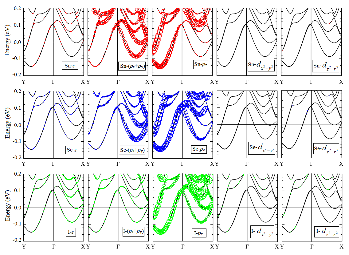
The microscopic origin of the spin-splitting in the impurity states can be understood by considering orbital hybridizations. Here, coupling between atomic orbitals contributes to the non-zero SOC matrix element through the relation , where is angular momentum resolved atomic SOC strength with , and are the orbital angular momentum and Pauli spin operators, and is the atomic orbitals. Therefore, only the orbitals with magnetic quantum number will contribute to the spin splitting. By calculating the orbital-resolved of the electronic band structures projected to the atom around the impurity site, we find that large spin splitting along the - line is mostly originated from the contribution of the () orbitals of the Sn, Se, and I atoms [Fig. 5]. On the contrary, along the line, the orbitals are dominated by the () orbitals, which contributes only minimally to the spin splitting. It is noted here that there is no contribution of the orbitals (, ) in the spin-split impurity bands, which is in contrast to halogen-doped TMDs ML Guo et al. (2017); Absor et al. (2018a) where the orbitals plays an important role for inducing the spin-split impurity bands.
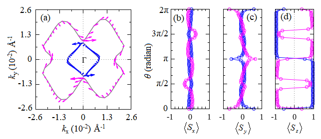
To clearly demonstrate the properties of the spin-split impurity bands, we calculate -space spin textures by using the spin density matrix of the spinor wave functions obtained from our DFT calculations. This method has previously been successfully applied on strained WS2 ML Absor et al. (2016), polar WSSe ML Absor et al. (2017) and WSTe ML Absor et al. (2018b) and halogen doped PtSe2 MLAbsor et al. (2018a). Here, we focus on the spin textures in the spin-split bands at Fermi level around the point [Fig. 4]. We find that the Fermi surface is characterized by the shifted two loops [Fig. 6(a)], dominated by the out-of-plane spin orientations [Figs. 6(b)-(d)]. These typical Fermi surface and spin textures indicate that the PSH states are achieved, which is similar to those observed on the (110)-oriented GaAs/AlGaAs QW Chen et al. (2014) and the ZnO (10-10) surface Absor et al. (2015). As mentioned previously that the I provides the in-plane electric field . This leads to the fact that the SOF is enforced to be parallel with spins in the out-of-plane direction. This inhibits the precession of the spins, thereby increasing the spin relaxation time. A similar mechanism behind long spin relaxation times has been reported on [110]-oriented zinc-blende QWs Döhrmann et al. (2004); Couto et al. (2007); Ohno et al. (1999); Chen et al. (2014), rendering that this system could provide an efficient spintronics device.
| Symmetry operation | (,,) | (,,) |
|---|---|---|
| (,,) | (,,) | |
| (,,) | (,,) |
The observed spin splitting and spin textures can be explained in term of an effective low-energy Hamiltonian, which can be deduced by considering the crystal symmetry. As mentioned previously that the relaxed comprises only a mirror symmetry [Fig. 1(c)]. Therefore, around the point, the wave vectors and spin vectors can be transformed according to the miror symmetry operator and time reversal symmetry operator , where is the is complex conjugation. The corresponding transformations for and are given in Table III. Collecting all the terms which are invariant with respect to the symmetry operations we obtain the effective Hamiltonian as follows Absor et al. (2015):
| (6) |
where ,, and are three independent coefficients and is the nearly free-electron energy. The Eq.(6) shows a combination between Rashba and Dresselhauss SOC with the coupling constants are given by and parameters, respectively, and one additional anisotropic (which is also referred as the anisotropic Drreselhauss term) parameter . Solving the eigenvalue problem involving the Hamiltonian of the Eq.(6), we find that
| (7) |
Morover, the spin textures can be deduced from the averaged components of the spinor operators , which is found to be
| (8) |
where and are defined by and , respectively, with is related to .
According to the Eq. (7), the PSH states is achieved when is zero. Therefore, the spin-orbit strength of the PSH . This means that the PSH states is purely characterized by the Dresselhauss effect, which is similar to the (110)-oriented QW. As a result, strong anisotropic spin splitting is observed, i.e., the band structure has large spin splitting along the (i.e ) line but is degenerated along the (i.e ) line, which is in fact consistent with our calculated result of spin-split bands shown in Fig. 4. By fitting the calculated band dispersion in Fig. 4 along the line with Eq.(7), we find that eVÅ. Moreover, from Eq. (8), we can estimate the ratio between and by comparing the in-plane and out-of-plane spin component along the line, and found that . Therefore, by using , we find that meVÅ and eVÅ. The larger value of indicates that the spin-split states are dominated by the out-of-plane spin component, which is also agree well with the calculated spin textures shown in Figs. 6(b)-(d).
| Systems | (eVÅ) | (nm) | Reference |
|---|---|---|---|
| SnSe-I ML | 1.76 | 1.27 | This work |
| SnSe-Br ML | 1.65 | 1.35 | This work |
| SnSe-Cl ML | 1.60 | 1.41 | This work |
| GaAs/AlGaAs QW | (3.5-4.9) | (7.3-10) | Ref.Walser et al. (2012) |
| 2.77 | 5.5 | Ref.Schönhuber et al. (2014) | |
| InAlAs/InGaAs QW | 1.0 | Ref.Ishihara et al. (2014) | |
| 2.0 | Ref.Sasaki et al. (2014) | ||
| CdTe QW | 5.6 | Ref.Passmann et al. (2018) | |
| ZnO(10-10) surface | 34.78 | 1.9 | Ref.Absor et al. (2015) |
| bulk BiInO3 | 1.91 | 2.0 | Ref.Sao and Tsymbal (2018) |
Now, we calculate another important parameter in the PSH states called as the wave length , which characterizes the spatially periodic mode Bernevig et al. (2006). Here, is defined as , where is the effective mass Bernevig et al. (2006). By analyzing the dispersion of the spin-split bands around the Fermi level along the - direction, we find that , where is the free electron mass, resulting in that is about 1.27 nm. The calculated is typically on the scale of the lithographic dimension used in the recent semiconductor industry Fiori et al. (2014).
We summarize the calculated results of the and in Table IV and compare the result with a few selected PSH materials from previously reported data. This revealed that the value of is much larger than those observed in the PSH of various zinc-blende -type QW structures such as GaAs/AlGaAs Walser et al. (2012); Schönhuber et al. (2014) and InAlAs/InGaAs Sasaki et al. (2014); Ishihara et al. (2014), ZnO (10-10) surfaceAbsor et al. (2015), strained LaAlO3/SrTiO3 (001) interface Yamaguchi and Ishii (2017), and is comparable with the recently reported PSH states on BiInO3 Sao and Tsymbal (2018). The large value of should ensure that a small is achieved. Indeed, the calculated value of is in fact three order less than that observed on the GaAs/AlGaAs QWs Walser et al. (2012); Schönhuber et al. (2014) and CdTe QWPassmann et al. (2018). Moreover, the calculated is much smaller than the electron coherence length (0.1m) measured at room temperature Wang and Jeng (2017), which is important for the development of a high-density scalable spintronics devices operating at room temperatures.
Thus far, we have found that the PSH with large spin splitting is achieved in the SnSe ML functionalized by a substitutional halogen doping. Because the PSH states is achieved on the spin-split bands near Fermi level [Fig. 3(c)], -type doping for spintronics is expected to be realized. Therefore, it enables us to allow operation as a spin-field effect transistor device at room temperature Yaji et al. (2009). It is noted here that our method for inducing the PSH states with large spin splitting can be extendable to other 2D monochalcogenide materials such as SnS, GeS, and GeSe where the electronic properties are similar Gomes et al. (2015). Therefore, this work provides a possible way to induce the PSH states with large spin splitting in the 2D nanomaterials, which is promising for future spintronic applications.
IV CONCLUSION
In summary, we have investigated the effect of a substitutional halogen doping on the electronic properties of the SnSe ML by employing the first-principles DFT calculations. We found that the substitutional halogen impurity can induce the PSH states with very large spin splitting, where -space Fermi surface is characterized by the shifted two loops exhibiting the out-of-plane spin orientations. We showed that these PSH states is originated from in-plane electric field induced by in-plane ferroelectric distortion. We clarified the properties of the PSH states in term of an effective Hamiltonian obtained from symmetry consideration. Recently, the doped group IV-monochalcogenides ML has been extensively studied Tang et al. (2018b); Wang et al. (2016). Our study clarified that the halogen doping plays an important role for inducing the PSH states in the electronic properties of the SnSe ML, which is expected to be useful for the development of an efficient and a high-density scalable spintronic devices operating at room temperatures. Finally, we expect that our theoretical predictions will stimulate experimental efforts in the exploration of the PSH in the 2D materials, which functional properties may be useful for future spintronic applications.
Acknowledgements.
The first authors (M. A. U. Absor) would like to thank T. Ozaki for his permission to use the computer facilities in the ISSP, the University of Tokyo, Japan, as a part of the ISS2018 summer school project. This work was partly supported by PDUPT 2018 Research Grant funded by the Ministry of Research and Technology and Higher Education (RISTEK-DIKTI), Republic of Indonesia.References
- Manchon et al. (2015) A. Manchon, H. C. Koo, J. Nitta, S. M. Frolov, and R. A. Duine, Nat. Matter 14, 871 (2015).
- Rashba (1960) E. I. Rashba, Sov. Phys. Solid State 2, 1224 (1960).
- Dresselhaus (1955) G. Dresselhaus, Phys. Rev. 100, 580 (1955).
- Dyakonov and Perel (1972) M. I. Dyakonov and V. I. Perel, Sov. Phys. Solid State 13, 3023 (1972).
- Datta and Das (1990) S. Datta and B. Das, Appl. Phys. Lett. 56, 665 (1990).
- Bernevig et al. (2006) B. A. Bernevig, J. Orenstein, and S.-C. Zhang, Phys. Rev. Lett. 97, 236601 (2006).
- Schliemann (2017) J. Schliemann, Rev. Mod. Phys. 89, 011001 (2017).
- Passmann et al. (2018) F. Passmann, S. Anghel, T. Tischler, A. V. Poshakinskiy, S. A. Tarasenko, G. Karczewski, T. Wojtowicz, A. D. Bristow, and M. Betz, Phys. Rev. B 97, 201413 (2018).
- Koralek et al. (2009) J. D. Koralek, C. P. Weber, J. Orenstein, B. A. Bernevig, S.-C. Zhang, S. Mack, and D. D. Awschalom, Nature 458, 610 (2009).
- Walser et al. (2012) M. P. Walser, C. Reichl, W. egscheider, and G. Salis, Nature Physics 8, 757 (2012).
- Kohda et al. (2012) M. Kohda, V. Lechner, Y. Kunihashi, T. Dollinger, P. Olbrich, C. Schönhuber, I. Caspers, V. V. Bel’kov, L. E. Golub, D. Weiss, K. Richter, J. Nitta, and S. D. Ganichev, Phys. Rev. B 86, 081306 (2012).
- Sasaki et al. (2014) A. Sasaki, S. Nonaka, Y. Kunihashi, M. Kohda, T. Bauernfeind, T. Dollinger, K. ARichter, and J. Nitta, Nature Nanotechnology 9, 703 (2014).
- Absor et al. (2015) M. A. U. Absor, F. Ishii, H. Kotaka, and M. Saito, Applied Physics Express 8, 073006 (2015).
- Yamaguchi and Ishii (2017) N. Yamaguchi and F. Ishii, Applied Physics Express 10, 123003 (2017).
- Sao and Tsymbal (2018) L. L. Sao and E. Y. Tsymbal, Nature Communications 9, 2763 (2018).
- Schönhuber et al. (2014) C. Schönhuber, M. P. Walser, G. Salis, C. Reichl, W. Wegscheider, T. Korn, and C. Schüller, Phys. Rev. B 89, 085406 (2014).
- Ishihara et al. (2014) J. Ishihara, Y. Ohno, and H. Ohno, Applied Physics Express 7, 013001 (2014).
- Chen et al. (2014) Y. S. Chen, S. Fält, W. Wegscheider, and G. Salis, Phys. Rev. B 90, 121304 (2014).
- Fei et al. (2016) R. Fei, W. Kang, and L. Yang, Phys. Rev. Lett. 117, 097601 (2016).
- Barraza-Lopez et al. (2018) S. Barraza-Lopez, T. P. Kaloni, S. P. Poudel, and P. Kumar, Phys. Rev. B 97, 024110 (2018).
- Zhang et al. (2014) C. Zhang, H. Yin, M. Han, Z. Dai, H. Pang, Y. Zheng, Y.-Q. Lan, J. Bao, and J. Zhu, ACS Nano 8, 3761 (2014).
- Li et al. (2013) L. Li, Z. Chen, Y. Hu, X. Wang, T. Zhang, W. Chen, and Q. Wang, Journal of the American Chemical Society 135, 1213 (2013), pMID: 23311291, https://doi.org/10.1021/ja3108017 .
- Xu et al. (2017) L. Xu, M. Yang, S. J. Wang, and Y. P. Feng, Phys. Rev. B 95, 235434 (2017).
- Shi and Kioupakis (2015) G. Shi and E. Kioupakis, Nano Letters 15, 6926 (2015), pMID: 26393677, https://doi.org/10.1021/acs.nanolett.5b02861 .
- Gomes and Carvalho (2015) L. C. Gomes and A. Carvalho, Phys. Rev. B 92, 085406 (2015).
- Guo et al. (2017) S. Guo, Y. Wang, C. Wang, Z. Tang, and J. Zhang, Phys. Rev. B 96, 245305 (2017).
- Absor et al. (2018a) M. A. U. Absor, I. Santoso, Harsojo, K. Abraha, H. Kotaka, F. Ishii, and M. Saito, Phys. Rev. B 97, 205138 (2018a).
- Perdew et al. (1996) J. P. Perdew, K. Burke, and M. Ernzerhof, Phys. Rev. Lett. 77, 3865 (1996).
- Ozaki et al. (2009) T. Ozaki, H. Kino, J. Yu, M. J. Han, N. Kobayashi, M. Ohfuti, F. Ishii, T. Ohwaki, H. Weng, and K. Terakura, http://www.openmx-square.org/ (2009).
- Troullier and Martins (1991) N. Troullier and J. L. Martins, Phys. Rev. B 43, 1993 (1991).
- Ozaki (2003) T. Ozaki, Phys. Rev. B 67, 155108 (2003).
- Ozaki and Kino (2004) T. Ozaki and H. Kino, Phys. Rev. B 69, 195113 (2004).
- Theurich and Hill (2001) G. Theurich and N. A. Hill, Phys. Rev. B 64, 073106 (2001).
- Popović et al. (2015) Z. S. Popović, J. M. Kurdestany, and S. Satpathy, Phys. Rev. B 92, 035135 (2015).
- Gomes et al. (2015) L. C. Gomes, A. Carvalho, and A. H. Castro Neto, Phys. Rev. B 92, 214103 (2015).
- Gomes et al. (2016) L. C. Gomes, A. Carvalho, and A. H. Castro Neto, Phys. Rev. B 94, 054103 (2016).
- Haleoot et al. (2017) R. Haleoot, C. Paillard, T. P. Kaloni, M. Mehboudi, B. Xu, L. Bellaiche, and S. Barraza-Lopez, Phys. Rev. Lett. 118, 227401 (2017).
- Wei and Zhang (2002) S.-H. Wei and S. B. Zhang, Phys. Rev. B 66, 155211 (2002).
- Tang et al. (2018a) C. Tang, Q. Li, C. Zhang, C. He, J. Li, T. Ouyang, H. Li, and J. Zhong, Journal of Physics D: Applied Physics 51, 245004 (2018a).
- Zhou et al. (2018a) Y. Zhou, W. Li, M. Wu, L.-D. Zhao, J. He, S.-H. Wei, and L. Huang, Phys. Rev. B 97, 245202 (2018a).
- Malone et al. (2014) B. D. Malone, A. Gali, and E. Kaxiras, Phys. Chem. Chem. Phys. 16, 26176 (2014).
- Ao et al. (2015) L. Ao, H. Y. Xiao, X. Xiang, S. Li, K. Z. Liu, H. Huang, and X. T. Zu, Phys. Chem. Chem. Phys. 17, 10737 (2015).
- Li et al. (2017) Z. Li, M. Liu, Q. Chen, Y. Huang, C. Cao, and Y. He, Superlattices and Microstructures 109, 829 (2017).
- Yanagi et al. (2016) H. Yanagi, Y. Iguchi, T. Sugiyama, T. Kamiya, and H. Hosono, Applied Physics Express 9, 051201 (2016).
- Zhou et al. (2018b) Y. Zhou, W. Li, M. Wu, L.-D. Zhao, J. He, S.-H. Wei, and L. Huang, Phys. Rev. B 97, 245202 (2018b).
- Yao et al. (2017) Q.-F. Yao, J. Cai, W.-Y. Tong, S.-J. Gong, J.-Q. Wang, X. Wan, C.-G. Duan, and J. H. Chu, Phys. Rev. B 95, 165401 (2017).
- Zhang and Schwingenschlögl (2018) Q. Zhang and U. Schwingenschlögl, Phys. Rev. B 97, 155415 (2018).
- Absor et al. (2016) M. A. U. Absor, H. Kotaka, F. Ishii, and M. Saito, Phys. Rev. B 94, 115131 (2016).
- Absor et al. (2017) M. A. U. Absor, I. Santoso, Harsojo, K. Abraha, H. Kotaka, F. Ishii, and M. Saito, Journal of Applied Physics 122, 153905 (2017).
- Absor et al. (2018b) M. A. U. Absor, H. Kotaka, F. Ishii, and M. Saito, Japanese Journal of Applied Physics 57, 04FP01 (2018b).
- Döhrmann et al. (2004) S. Döhrmann, D. Hägele, J. Rudolph, M. Bichler, D. Schuh, and M. Oestreich, Phys. Rev. Lett. 93, 147405 (2004).
- Couto et al. (2007) O. D. D. Couto, F. Iikawa, J. Rudolph, R. Hey, and P. V. Santos, Phys. Rev. Lett. 98, 036603 (2007).
- Ohno et al. (1999) Y. Ohno, R. Terauchi, T. Adachi, F. Matsukura, and H. Ohno, Phys. Rev. Lett. 83, 4196 (1999).
- Fiori et al. (2014) G. Fiori, F. Bonaccorso, G. Iannaccone, T. Palacios, D. Neumaier, A. Seabaugh, S. K. Banerjee, and L. Colombo, Nature Nanotechnology 83, 768 (2014).
- Wang and Jeng (2017) T.-H. Wang and H.-T. Jeng, npj Computational Materials 3, 5 (2017).
- Yaji et al. (2009) K. Yaji, Y. Ohtsubo, S. Hatta, H. Okuyama, K. Miyamoto, T. Okuda, A. Kimura, H. Namatame, M. Taniguci, and T. Aruga, Nat. Commn. 1, 1016 (2009).
- Tang et al. (2018b) C. Tang, Q. Li, C. Zhang, C. He, J. Li, T. Ouyang, H. Li, and J. Zhong, Journal of Physics D: Applied Physics 51, 245004 (2018b).
- Wang et al. (2016) Q. Wang, W. Yu, X. Fu, C. Qiao, C. Xia, and Y. Jia, Phys. Chem. Chem. Phys. 18, 8158 (2016).