Centre for Advanced 2D Materials and Graphene Research Centre \alsoaffiliationDepartment of Physics, National University of Singapore \alsoaffiliationCentre for Advanced 2D Materials and Graphene Research Centre \alsoaffiliationDepartment of Chemistry, National University of Singapore \alsoaffiliationCentre for Advanced 2D Materials and Graphene Research Centre \alsoaffiliationDepartment of Physics, National University of Singapore
Elastomeric waveguide on-chip coupling of an encapsulated MoS2 monolayer
Abstract
We propose a robust photonic platform for encapsulation and addressing of optically active 2D- and nano-materials. Our implementation utilises a monolayer of MoS2 transition metal dichalcogenide embedded in an elastomeric waveguide chip. The structure is manufactured from PDMS using soft-lithography and capable of sustaining a single mode of guided light. We prove that this setup facilitates addressing of the 2D material flake by pumping it with polarised laser light and gathering polarisation-resolved photoluminescence spectra with the extinction ratio of 31, which highlights the potential for selection-rule dependent measurements. Our results demonstrate improved handling of the material and experimental simplification compared to other techniques. Furthermore, inherent elasticity of the host provides an avenue for direct mechanical coupling to embedded materials.

Advances in the fundamental understanding of ultra-thin transition metal dichalcogenides (TMDs) including their excitonic properties 1, exciton-phonon coupling 2, optical selection rules 3 and valley degree of freedom 4, position them as attractive candidates for components of devices in novel photonic and optoelectronic applications 5, 6, 7, 8. Monolayer materials are fragile and difficult to handle due to the micrometer footprint and their tendency to crumple. In order to incorporate them in the existing photonic systems, there is a need for packaging in the form of a robust platform for handling and testing of the material. Planar photonic waveguide chips capable of confining light on the micrometer scale are a natural candidate for such a platform, offering transmission of visible light, polarisation selectivity and shielding from environmental influence. While this is challenging to achieve with traditional semiconductor or glass waveguide structures, we propose that a photonic device fabricated in an elastomer can serve as a host for encapsulation of the monolayers and their heterostructures. Using the suggested geometry, we show it is feasible to confine an optically active 2D material within the mode of guided light, allowing for the propagation of linearly polarised light in the plane of the monolayer. As reported previously 9 such waveguides are capable of guiding orthogonal polarization states with very similar mode profiles. This allows the polarisation of light in this system to be changed such that exciton states with different optical selection rules (e.g. dark and bright excitons) can be independently accessed. Embedding the material of interest in an elastomer gives an added benefit of direct mechanical coupling by performing either global or local deformation of the chip.
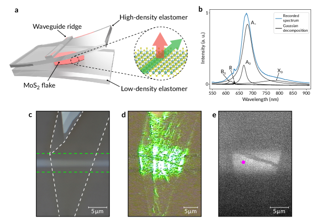
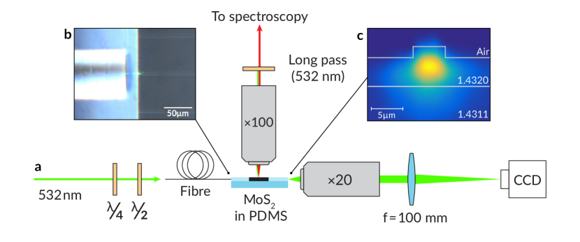
Here, we describe a proof-of-concept device, utilising a monolayer of MoS2 encapsulated within the mode of light guided in a polydimethylsiloxane (PDMS) chip. A stylised illustration of the experimental sample (Figure 1a) shows an MoS2 flake inserted between the two layers of PDMS. Different refractive indices of the layers (1.4320 and 1.4311, simulated), together with the geometry of the top ridge, create a light-guiding structure capable of sustaining a single mode of radiation (see inset in Figure 2 for an image of the guided mode). Positioning a flake of 2D material within the mode of the guided light allows for efficient coupling. Here, we demonstrate this experimentally for a flake of MoS2 by exciting it through the waveguide and performing room temperature measurement of the photoluminescence spectrum while varying the polarisation of incident light.
0.1 Experiment
The experimental setup for the excitation and collection of PL spectra is shown in Figure 2. laser light is coupled to a single-mode fibre, which is cut and stripped at one end to expose the core and cladding. The exposed end is mounted on a micrometre stage (Newport ULTRAlign XYZ + yaw, pitch, roll) and aligned to couple to the chip waveguide that encapsulates the MoS2 flake. Coupling is optimised by maximising the transmitted power collected by the imaging objective on the opposite end of the chip (). The incident light couples to the MoS2 monolayer and the resulting photoluminescence is collected by a high NA top-down objective (), after passing through the long-pass filter to eliminate the excitation wavelength. To achieve linear polarization at the location of the MoS2 flake, strain-induced birefringence in the single mode fibre (and to a lesser extent the waveguide itself) is pre-compensated using a quarter wave plate and half wave plate. Once completed, the polarization of the excitation beam at the location of the flake can be rotated in the linear basis by additional rotation of the half wave plate alone.

0.2 Results
The encapsulated flake is investigated in detail by spatial mapping of the photoluminescence spectrum by normal excitation, which shows the distribution of the integrated photoluminescence, linewidth broadening and the peak position for the spectral range (Figures 3a, b and c respectively). Figure 3a reveals the integrated photoluminescence spectrum map for the area of the flake within and around the edges of the waveguide ridge, with variations that can be attributed to the spatial inhomogeneity of the flake. This is likely due to wrinkles formed during the fabrication of the low-density elastomer layer of the waveguide. There is a correlation between the linewidth distribution and the photoluminescence intensity (compare Figure 3a and b), with narrow emission implying high area and intensity.

The map of the peak distribution (Figure 3c) shows a strong correlation with the waveguide geometry, with the two regions of interest separated by the edges of the waveguide ridge. The photoluminescence peak undergoes a red shift of between the outer region towards the waveguide ridge. Figure 3d shows extracted photoluminescence spectra from different regions of the monolayer flake. Such spectrum mainly consists of the ground exciton peak 10 originating from the direct optical transition at the K and K’ points of the Brillouin zone. 11, 12 The strong asymmetric photoluminescence peak is made of two contributions: neutral (A0) and charged (A-) excitons 13, 14 separated by 45 meV (See Fig. 1b). Noticeably, relative intensities of these two peaks vary spatially, resulting in the apparent changes of the cumulative line-shape. Similar modifications of the optical properties have been reported for uniaxially 2 and biaxially 15 strained monolayer of MoS2.
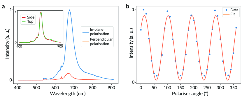
Subsequently, we study the polarisation dependence of the photoluminescence spectra, which are obtained by parallel excitation of the flake with incident pump light delivered to the material through the waveguide (see call-out in Figure 1a). A monolayer of MoS2 is pumped with in-plane laser light to induce the primary photoexcitations (excitons) (Figure 4a). The resultant photoluminescence spectrum is collected from the probing region (Figure 1e) and reveals the typical characteristics of monolayer MoS2.
Polarisation parallel to the flake surface produced maximum excitation (photoluminescence) and conversely, orthogonal polarisation minimised the excitation (see Figure 4a for comparison of intensities). This is in agreement with the two-dimensional nature of the bright excitons, that offer maximum cross section for polarisation of light when it is parallel to the flake 16. By rotating the polarisation of the incident light, the excitonic emission is not completely extinguished. Assuming the finite theoretical limit of the extinction, we speculate it is further reduced due to the irregularities in the monolayer surface (introduced during the dry-stamping transfer process), which act as scattering centres, visible in Figure 1d. Similar photoluminescence curves are recorded for intermediate values of polarisation in the increments of . The resultant spectra are integrated, normalised for power (to mitigate the laser instabilities) and plotted against the polarisation angle (Figure 4b). Power for the normalisation is recorded after passing through the chip, at the position of a CCD sensor (Figure 2). The normalised points are then fitted to a sine function that demonstrates the polarisation dependence of photoluminescence with high extinction ratio of 31 between parallel and perpendicular states, which compares favourably with previous reports 17.
In addition, we have performed measurements of photoluminescence at the end face of the chip comparing two identical waveguides, one of which contained the flake. The flake generates bright exciton emission at a normal to its plane, which does not couple back into the guided mode and we have indeed observed no resolvable photoluminescence signal at the output of the waveguide. Further to this, we aim to extend the experiment to investigate emission of the dark exciton in MoS2 and other dichalcogenide monolayers 1, 3, which has the potential for waveguide out-coupling in our geometry.

0.3 Conclusion
We have presented a working prototype of a photonic chip with an atomically thin MoS2 flake, which is encapsulated directly within the single mode of guided laser light. The observed photoluminescence spectra are consistent with the ones present in the literature for monolayers of MoS2. Sensitivity of the photoluminescence signal to polarisation of pump light is shown, with high extinction ratio and exact expected periodicity of . The chip has shown robustness and ease of handling, being reused in multiple experiments over a period of months without any noticeable degradation in the MoS2 flake. Such capabilities can enable further experiments dealing with optically active materials, such as 2D monolayers, nano-diamonds, crystalline and organic single photon emitters, and similar.
0.4 Methods
The elastomeric waveguide chip is fabricated out of polydimethylsiloxane (PDMS) in a two-step soft lithography process 9, with an additional step for material encapsulation. A lithographic mould is prepared by defining by waveguides on a silicon wafer using laser direct-write in the photoresist (AZ1512HS, AZ Electronic Materials). The PDMS liquid precursor is spun onto the mould and cured at to create a thick high-density layer. The MoS2 flake is transferred to the cured PDMS layer at the location of a waveguide, using dry-stamping technique 18. of PDMS liquid precursor is then poured on the top of the structure and cured at to form a low-density layer and provide a structural base for the chip. The chip is then peeled from the silicon substrate and end-faces are cut using a microtome blade to enable coupling of an optical fibre. Optical microscope images of the encapsulated flake are shown in Figure 1c to e.
MoS2 was exfoliated from the bulk single-crystal flake (SPI) by the scotch-tape method onto the surface of the clean home-made PDMS slab. The monolayer was identified by contrast, photoluminescence and Raman spectroscopy. Selected flake was then encapsulated in the PDMS waveguide, as explained above.
0.5 Funding statement
G.E. acknowledges the Singapore National Research Foundation for funding the research under medium-sized centre programme. G.E. also acknowledges support from the Ministry of Education (MOE), Singapore, under AcRF Tier 2 (MOE2015-T2-2-123, MOE2017-T2-1-134) and AcRF Tier 1 (R-144-000-387-114). A.L., F.A., J.A.G. and K.F.N. acknowledge support from the Ministry of Education (MOE), Singapore under AcRF Tier 3 (MOE2012-T3-1-009) and the National Research Foundation, Prime Minister’s Office, Singapore under its Research Centres of Excellence programme.
References
- Robert et al. 2017 Robert, C.; Amand, T.; Cadiz, F.; Lagarde, D.; Courtade, E.; Manca, M.; Taniguchi, T.; Watanabe, K.; Urbaszek, B.; Marie, X. Fine structure and lifetime of dark excitons in transition metal dichalcogenide monolayers. Phys. Rev. B 2017, 96, 155423
- Niehues et al. 2018 Niehues, I. et al. Strain Control of Exciton–Phonon Coupling in Atomically Thin Semiconductors. Nano Lett. 2018, 18, 1751–1757
- Wang et al. 2017 Wang, G.; Robert, C.; Glazov, M. M.; Cadiz, F.; Courtade, E.; Amand, T.; Lagarde, D.; Taniguchi, T.; Watanabe, K.; Urbaszek, B.; Marie, X. In-Plane Propagation of Light in Transition Metal Dichalcogenide Monolayers: Optical Selection Rules. Phys. Rev. Lett. 2017, 119, 047401
- Xu et al. 2014 Xu, X.; Yao, W.; Xiao, D.; Heinz, T. F. Spin and pseudospins in layered transition metal dichalcogenides. Nat. Phys. 2014, 10, 343
- Vella et al. 2017 Vella, D.; Ovchinnikov, D.; Martino, N.; Vega-Mayoral, V.; Dumcenco, D.; Kung, Y.-C.; Antognazza, M.-R.; Kis, A.; Lanzani, G.; Mihailovic, D.; Gadermaier, C. Unconventional electroabsorption in monolayer MoS 2. 2D Mater. 2017, 4, 021005
- Huo et al. 2017 Huo, N.; Yang, Y.; Li, J. Optoelectronics based on 2D TMDs and heterostructures. J. Semicond. 2017, 38, 031002
- Hill et al. 2017 Hill, H. M.; Rigosi, A. F.; Raja, A.; Chernikov, A.; Roquelet, C.; Heinz, T. F. Exciton broadening in /graphene heterostructures. Phys. Rev. B 2017, 96, 205401
- Jiang and Park 2014 Jiang, J.-W.; Park, H. S. Mechanical properties of /graphene heterostructures. Appl. Phys. Lett. 2014, 105, 033108
- Grieve et al. 2017 Grieve, J. A.; Ng, K. F.; Rodrigues, M. J. L. F.; Viana-Gomes, J.; Ling, A. Mechanically tunable integrated beamsplitters on a flexible polymer platform. Appl. Phys. Lett. 2017, 111, 211106
- Splendiani et al. 2010 Splendiani, A.; Sun, L.; Zhang, Y.; Li, T.; Kim, J.; Chim, C.-Y.; Galli, G.; Wang, F. Emerging Photoluminescence in Monolayer . Nano Lett. 2010, 10, 1271–1275
- Mak et al. 2010 Mak, K. F.; Lee, C.; Hone, J.; Shan, J.; Heinz, T. F. Atomically Thin : A New Direct-Gap Semiconductor. Phys. Rev. Lett. 2010, 105, 136805
- Chhowalla et al. 2013 Chhowalla, M.; Shin, H.; Eda, G.; Li, L.; Loh, K.; Zhang, H. The chemistry of two-dimensional layered transition metal dichalcogenide nanosheets. Nat. Chem. 2013, 5, 263
- Mak et al. 2013 Mak, K. F.; He, K.; Lee, C.; Lee, G. H.; Hone, J.; Heinz, T. F.; Shan, J. Tightly bound trions in monolayer . Nat. Mater. 2013, 12, 207–11
- Chernikov et al. 2015 Chernikov, A.; van der Zande, A. M.; Hill, H. M.; Rigosi, A. F.; Velauthapillai, A.; Hone, J.; Heinz, T. F. Electrical Tuning of Exciton Binding Energies in Monolayer . Phys. Rev. Lett. 2015, 115, 126802
- Lloyd et al. 2016 Lloyd, D.; Liu, X.; Christopher, J. W.; Cantley, L.; Wadehra, A.; Kim, B. L.; Goldberg, B. B.; Swan, A. K.; Bunch, J. S. Band Gap Engineering with Ultralarge Biaxial Strains in Suspended Monolayer . Nano Lett. 2016, 16, 5836–5841
- Schuller et al. 2013 Schuller, J. A.; Karaveli, S.; Schiros, T.; He, K.; Yang, S.; Kymissis, I.; Shan, J.; Zia, R. Orientation of luminescent excitons in layered nanomaterials. Nat. Nanotechnol. 2013, 8, 271
- Tan et al. 2014 Tan, Y.; He, R.; Cheng, C.; Wang, D.; Chen, Y.; Chen, F. Polarization-dependent optical absorption of for refractive index sensing. Sci. Rep. 2014, 4, 7523
- Castellanos-Gomez et al. 2014 Castellanos-Gomez, A.; Buscema, M.; Molenaar, R.; Singh, V.; Janssen, L.; Van der Zant, H. S.; Steele, G. A. Deterministic transfer of two-dimensional materials by all-dry viscoelastic stamping. 2D Mater. 2014, 1, 011002