Memristive LSTM network hardware architecture for time-series predictive modeling problems
Abstract
Analysis of time-series data allows to identify long term trends and make predictions that can help to improve our lives. With rapid development of artificial neural networks, long short-tern memory (LSTM) recurrent neural network (RNN) configuration is found to be capable in dealing with time-series forecasting problems where data points are time dependent and possess seasonality trends. Gated structure of LSTM cell and flexibility in network topology (one-to-many, many-to-one, etc) allows to model systems with multiple input variables and control several parameters such as the size of look-back window to make a prediction and number of time steps to be predicted. These make LSTM attractive tool over conventional methods such as auto regression models, simple average, moving average, naive approach, ARIMA, Holt’s linear trend method, Holt’s Winter seasonal method, and others. In this paper, we propose a hardware implementation of LSTM network architecture for time-series forecasting problem. All simulations were performed using TSMC 0.18 m CMOS technology and HP memristor model.
Index Terms:
LSTM, RNN, memristor, crossbar, analog circuit, time-series predictionI Introduction
First introduced in 1995 [1], long short-term memory (LSTM) is a special configuration of RNN aimed to bypass exploding or vanishing gradient problems in conventional RNN. This became possible due to the gated structure of an LSTM cell which allows to control the flow of current and previous cell’s data. As RNN, LSTM network has feedback connections to retain order of information which makes it powerful tool for processing sequential data. Various applications where LSTM networks have been successfully used include machine translation, speech recognition, forecasting, and others[2],[3], [4]. Most of them are mainly software-based and few works on FPGA are introduced [5], [6]. However, their implementation is still limited due to large complexity and parallelism of LSTM network structure that requires huge computational resources.
Previous work [7] offered CMOS-memristor analog circuit design of current-based LSTM cell architecture for time-series prediction problem by [8]. It used current mirrors and current-based activation function circuits. In this work, we propose voltage-based circuits since they provide us with higher accuracy and more predictable outputs. Current-based implementation could be used in solving a classification problem. This is because we are not interested in the analog output voltage – as long as it is high enough or low enough, we know that it is either digital “1” or digital “0”. Whereas, in the case of time series prediction problem, we are interested in the analog output voltage to be much accurate rather than it being higher or lower of some threshold value. Therefore, high-accuracy sigmoid and hyperbolic tangent function circuits, which are voltage-based, were implemented. In addition, high accuracy four-quadrant multiplier circuit was adapted from [9]. They help to obtain accurate values at each stage to finally arrive to an accurate output value. Additionally, control circuit has been implemented to carry out the multiple time step feature of the LSTM RNN.
It is a fact that time series prediction will yield some error, for instance mean square error (MSE) or root mean square error (RMSE). If the RMSE of the circuit and the software implementations are close enough, then we can conclude that we successfully implemented the LSTM neural network in analog hardware.
This paper is structured as following: first, problem description along with LSTM overview is given; further each major circuit parts are introduced; and finally simulation results are presented and conclusions are drawn.
II Proposed circuit
II-A Problem description and LSTM overview
Proposed circuit design implements time-series prediction problem using LSTM by Brownlee [8]. The provided dataset demonstrates the change of the number of international airline passengers during 12 year period with 144 observation points. Prior being processed, it was divided into training and testing sets and normalized between 0 and 1 due to the sensitivity of LSTM to input data. The single-column data-set is converted into three-column, where the first column contains information on the number of passengers in the previous month, the second column in the current month and the third column is the number of passengers to be predicted (Table I).
| Original data | Normalized data | ||||
| X(t-1) | X(t) | X(t+1) | X(t-1) | X(t) | X(t+1) |
| 112 | 118 | 132 | 0.015444 | 0.027027 | 0.054054 |
| 118 | 132 | 129 | 0.027027 | 0.054054 | 0.048263 |
| 132 | 129 | 121 | 0.054054 | 0.048263 | 0.032819 |
| 129 | 121 | 135 | 0.048263 | 0.032819 | 0.059846 |
| … | … | … | … | … | … |
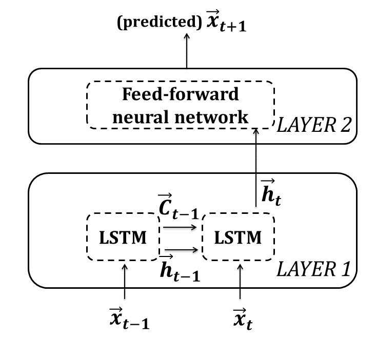
Fig.1 shows a diagram for the implementation of the task. It consists of two layers, where the first layer is LSTM network with two time-steps and four hidden units and the second layer is a feed-forward neural network with linear activation function.
A closer look into an LSTM cell structure can be seen in the Fig. 2. The input data of LSTM unit is a concatenated vector of new input data and data from a previous cell . Biases are used to identify zero inputs. The concatenated vector is multiplied by a weight matrix and obtained outputs go through activation functions (either sigmoid or hyperbolic tangent) to form gate values. The output values of forget gate after sigmoid layer is between 0 and 1. Hadamard multiplication of with previous cell state is used to decide whether to keep or partially/completely delete information on in the current cell. Similarly the input gate output contributes to the new cell state by deciding to block or pass a new candidate cell state . Combination of some part of new and some part of old information then produces new candidate cell state mathematically shown in (4). Eventually, output gate decides how much of the filtered version of forms a new cell output as shown in (6). is filtered through hyperbolic tangent function to have the outputs between -1 and 1.
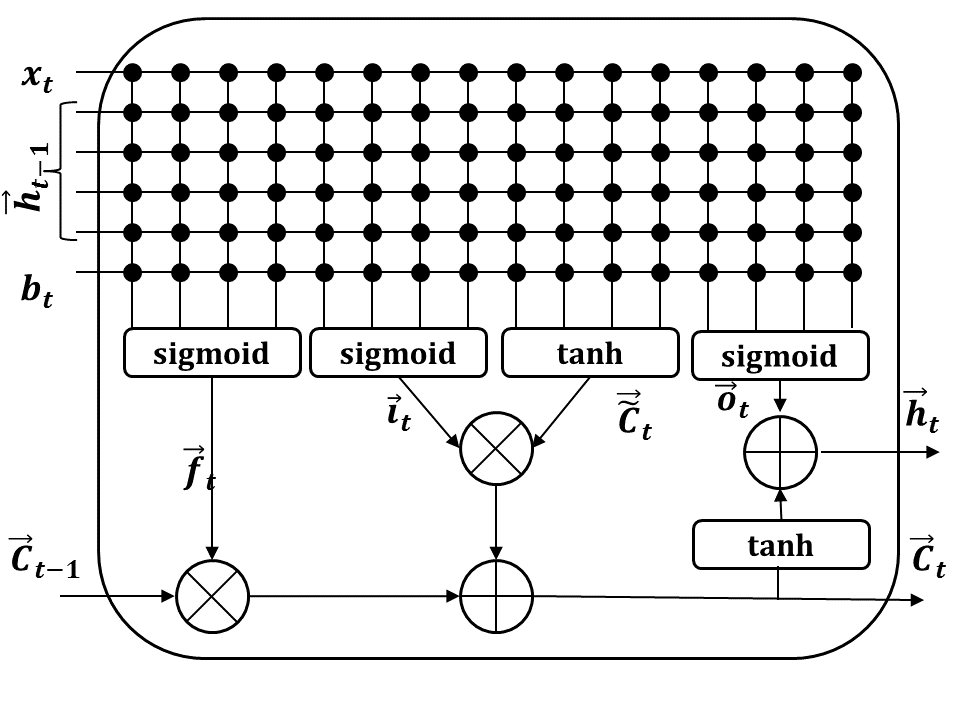
Operation of LSTM cell can be described by following equations [10]:
| (1) |
| (2) |
| (3) |
| (4) |
| (5) |
| (6) |
Since the number of hidden units in our LSTM cell is chosen to be four, the size of matrices , , and are [4x4]. And sizes of matrices , , , , , , and are [1x4]. The resulting size of the matrix in a LSTM unit for the given problem is [6x16]. Weights and biases were constrained to the range [-1;1]. Upon training in Python Keras, their values were extracted to build the circuit.
II-B Vector-matrix multiplication circuit
In hardware, weight matrix of LSTM cell can be implemented using memristor crossbar array [11], [12]. Memristor is a non-volatile element capable of remembering its resistance state. Typically it has two states and that can be controlled by applied voltage amplitude and pulse duration. Memristor existence was postulated by L.Chua back in 1971 [13] and HP Labs announced its in 2008 [14], [15]. It is a promising element due to nanoscale size, absence of leakage current and reprogramming ability. Using memristors in a crossbar array to perform vector-matrix multiplication benefits in fast computational speed and small area.
Since weight value in LSTM cell can take both positive and negative values, it can be represented as a difference of two memristor conductances [16]. This doubles the number of memristors in a matrix. and of memristors were chosen to be 10k and 10M, respectively. Fig.3 shows implementation of forget gate of the LSTM cell. Similar approach can be used to construct the rest of the gates.
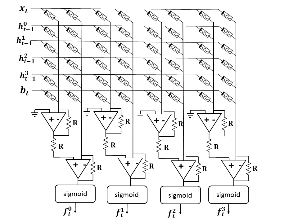
The vector-matrix multiplication circuit input (input, hidden unit) values are the same as for the software implementation case between 0 and 1. Only exception is bias input values (not bias weights, though weights can be adjusted accordingly) in the circuit are higher by 0.3V in the LSTM layer and by 0.25V in the dense layer than that of bias input values obtained from the software implementation. It is done to make up for the stage-wise loss of voltage values that propagate through the circuit. The bias input value in LSTM layer is 1.5 and in the dense (feed-forward neural network) layer is 0.0239 (in software).
II-C Sigmoid and hyperbolic tangent function circuits
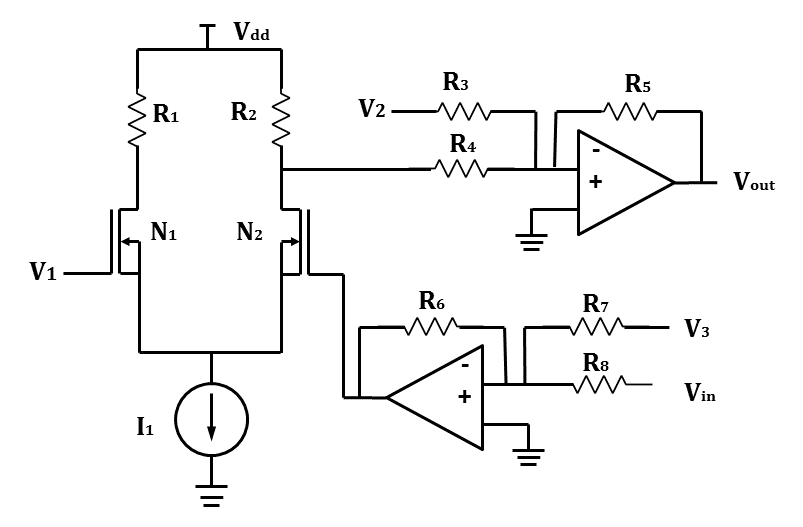
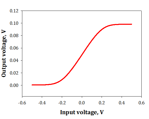
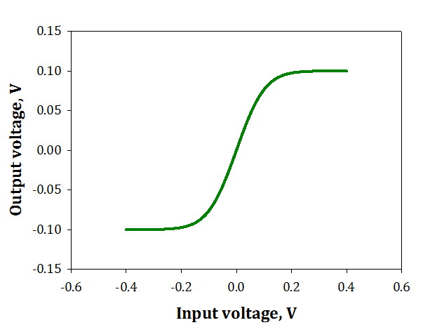
Sigmoid and hyperbolic tangent functions can be obtained using circuit in Fig. 4. It basically employs the property of differential amplifier – gradual and smooth increase of the output voltage when the differential input is swept between a desired range. The desired output range and form can be obtained by varying supply voltage , current , and the sizes of NMOS transistors ( and ). Voltage source values of , , and are used to shift the output values to match the graphs of the sigmoid and hyperbolic tangent functions. Since these two functions are different, the above mentioned parameters also change for each function. DC transfer characteristics for sigmoid and hyperbolic tangent function circuits are shown in Fig.7 and Fig.7, respectively. The graphs’ input and output ranges are scaled down by -10 (negative part is canceled at later stages) to meet the operation range of the other circuit elements.
II-D Four-quadrant multiplier circuit
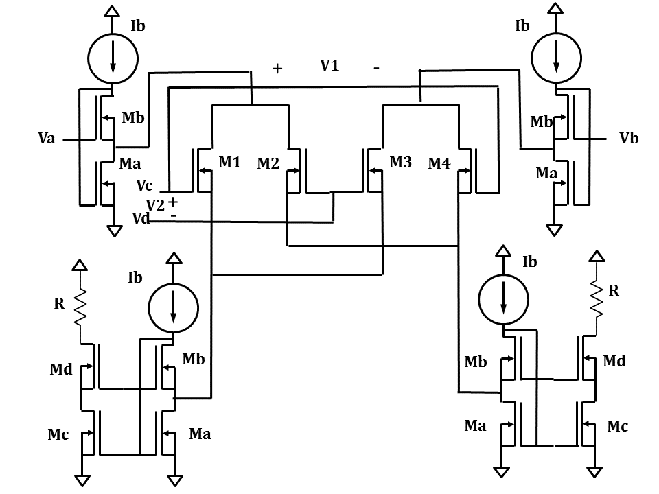
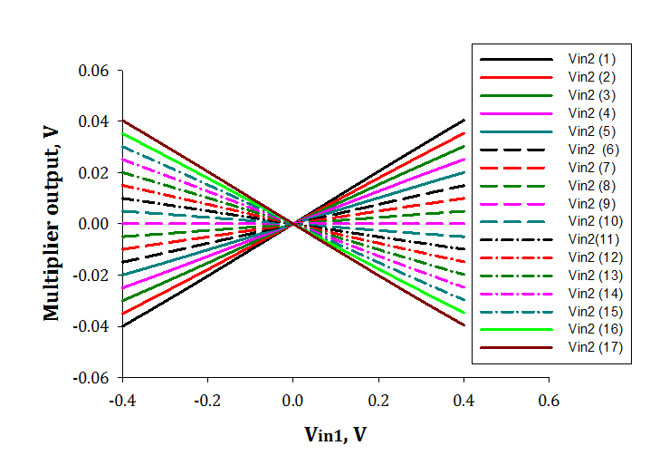
Fig. 5 shows a low-voltage four quadrant transconductance CMOS multiplier from [9]. Its core cell consists of NMOS transistors M1-M4. Current source and transistors and form a flipped voltage follower cell. It is characterized by low impedance for current sensing purposes. The multiplier circuit was further extended to have single-ended output. It has been done by scaling down the source voltages of transistors , then amplifying their difference, and finally shifting plus amplifying the amplified difference to get highly accurate output value. In addition, current sources in Fig. 5 were replaced with its CMOS implementations. Voltage transfer characteristics of the multiplier circuit is shown Fig. 8. The outputs are scaled down by -4 for the same reason as in the activation function circuits.
III Simulation results
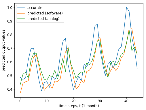
Simulation performance results obtained from software and hardware (analog) closely match as seen in Fig. 6 and both of them repeat the general trend in the plot. Numerical comparison reveals that MSE and RMSE for the software prediction are 0.0112 and 0.1059, respectively. While, MSE and RMSE for the analog prediction are 0.0101 and 0.1004, respectively.
The total circuit simulation time for predicting 45 test points is 3.96 ms with each cycle taking 88 s. First 40 microseconds are spent for the computation of and for all four units with 10 s being a sub-cycle of computing outputs of a single hidden unit. In fact, 2 microseconds of those 10 microseconds are used as an intentional delay to avoid convergence issues. Sub-cycles are realized using pass-logic circuits and corresponding control signals. At the end of each sub-cycle time, the outputs are stored at memory circuits consisting of op-amp buffer and a capacitor. They are to be used in the second time step calculations. After the first time step ends, intentional 2 s delay is inserted. The next 40 s starting from 42 s to 82 s are used for the computation of and for all hidden units in the same sub-cycle manner. Again after the second time step, 2 s delay is introduced. Starting from 84 s to 87 s, the circuit computes the final output value - time series prediction value. Final stage is given short time interval of 3 s, because the circuit computes only the weighted sum of through a dense layer and adds a bias to it. Lastly, 1 s intentional delay is introduced and the first cycle ends.
Total maximum power consumption for a single LSTM cell is 210.67 mW when all the inputs ( and ) are set to 1V and the bias input is set to 1.8V; and its area is 58569.
IV Conclusion
This paper proposed voltage-based LSTM circuit design for predicting the number of international airplane passengers. Having voltage-based LSTM circuit reduces the overhead of converting between currents and voltages which significantly reduces circuit area and complexity. In addition, it makes it easy to adjust the intermediate node voltages to desired voltage values during the stage-wise building of the circuit. From obtained simulation results, it is clear that the prediction results closely match between the hardware and software implementations. Simulation times can be further reduced by adjusting the control voltage signals by making sure that there are no convergence issues.
References
- [1] S. Hochreiter and J. Schmidhuber, “Long short-term memory,” Neural computation, vol. 9, no. 8, pp. 1735–1780, 1997.
- [2] S. Xingjian, Z. Chen, H. Wang, D.-Y. Yeung, W.-K. Wong, and W.-c. Woo, “Convolutional lstm network: A machine learning approach for precipitation nowcasting,” in Advances in neural information processing systems, 2015, pp. 802–810.
- [3] A. Graves, N. Jaitly, and A.-r. Mohamed, “Hybrid speech recognition with deep bidirectional lstm,” in Automatic Speech Recognition and Understanding (ASRU), 2013 IEEE Workshop on. IEEE, 2013, pp. 273–278.
- [4] D. Soutner and L. Müller, “Application of lstm neural networks in language modelling,” in International Conference on Text, Speech and Dialogue. Springer, 2013, pp. 105–112.
- [5] S. Han, J. Kang, H. Mao, Y. Hu, X. Li, Y. Li, D. Xie, H. Luo, S. Yao, Y. Wang et al., “Ese: Efficient speech recognition engine with sparse lstm on fpga,” in Proceedings of the 2017 ACM/SIGDA International Symposium on Field-Programmable Gate Arrays. ACM, 2017, pp. 75–84.
- [6] Y. Guan, Z. Yuan, G. Sun, and J. Cong, “Fpga-based accelerator for long short-term memory recurrent neural networks,” in Design Automation Conference (ASP-DAC), 2017 22nd Asia and South Pacific. IEEE, 2017, pp. 629–634.
- [7] K. Smagulova, K. Adam, O. Krestinskaya, and A. P. James, “Design of cmos-memristor circuits for lstm architecture,” arXiv preprint arXiv:1806.02366, 2018.
- [8] J. Brownlee, “Time series prediction with lstm recurrent neural networks in python with keras,” Available at: machinelearningmastery. com, 2016.
- [9] J. Ramirez-Angulo, S. Thoutam, A. Lopez-Martin, and R. Carvajal, “Low-voltage cmos analog four quadrant multiplier based on flipped voltage followers,” in Circuits and Systems, 2004. ISCAS’04. Proceedings of the 2004 International Symposium on, vol. 1. IEEE, 2004, pp. I–681.
- [10] C. Olah, “Understanding lstm networks,” GITHUB blog, posted on August, vol. 27, p. 2015, 2015.
- [11] K. Smagulova, O. Krestinskaya, and A. P. James, “A memristor-based long short term memory circuit,” Analog Integrated Circuits and Signal Processing, vol. 95, no. 3, pp. 467–472, 2018.
- [12] A. Irmanova and A. P. James, “Multi-level memristive memory with resistive networks,” in Postgraduate Research in Microelectronics and Electronics (PrimeAsia), 2017 IEEE Asia Pacific Conference on. IEEE, 2017, pp. 69–72.
- [13] L. Chua, “Memristor-the missing circuit element,” IEEE Transactions on circuit theory, vol. 18, no. 5, pp. 507–519, 1971.
- [14] R. S. Williams, “How we found the missing memristor,” IEEE spectrum, vol. 45, no. 12, 2008.
- [15] D. B. Strukov, G. S. Snider, D. R. Stewart, and R. S. Williams, “The missing memristor found,” nature, vol. 453, no. 7191, p. 80, 2008.
- [16] R. Hasan, T. M. Taha, and C. Yakopcic, “On-chip training of memristor crossbar based multi-layer neural networks,” Microelectronics Journal, vol. 66, pp. 31–40, 2017.