∎
22email: li_lu@mymail.sutd.edu.sg 33institutetext: Weiling Dong 44institutetext: Singapore University of Technology and Design, 8 Somapah Road, Singapore, 487372
44email: weiling_dong@mymail.sutd.edu.sg 55institutetext: Jitendra K. Behera 66institutetext: Singapore University of Technology and Design, 8 Somapah Road, Singapore, 487372
66email: jitendra_behera@mymail.sutd.edu.sg 77institutetext: Li Tian Chew 88institutetext: Singapore University of Technology and Design, 8 Somapah Road, Singapore, 487372
88email: litian_chew@sutd.edu.sg 99institutetext: Robert E. Simpson 1010institutetext: Singapore University of Technology and Design, 8 Somapah Road, Singapore, 487372
Tel.: +65 64994519
1010email: robert_simpson@sutd.edu.sg
Supporting information
1 Diffusion profile of Au/Ge2Sb2Te5
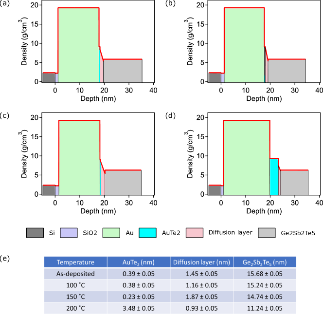
The modelled diffusion profiles of Au/Ge2Sb2Te5 in the as-deposited state and after annealing at 100 , 150 , and 200 are shown in Figure S1 (a)–(d). The thickness and roughness of the Au/Ge2Sb2Te5 diffusion layer in the as-deposited state and after annealing at 100 , 150 , and 200 are shown in Figure S1 (e).

The model structure consists of a silicon substrate, a thermal silicon dioxide layer, a Au layer, a AuTe2 layer, a diffusion layer, and a Ge2Sb2Te5 layer. The silicon dioxide layer is due to the thermal oxidation of the silicon substrate. The diffusion layer is modelled as a gradient layer with the density changing from the density of AuTe2 to the density of Ge2Sb2Te5.
2 XRD pattern of TiN/Ge2Sb2Te5
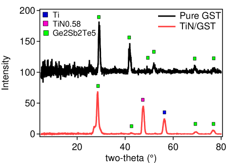
The XRD patterns from TiN/Ge2Sb2Te5 and Ge2Sb2Te5 after annealing at 200 are shown in Figure S2.

The XRD peaks of TiN/Ge2Sb2Te5 are in accordance with face centered cubic Ge2Sb2Te5 in the crystalline state. There are also Ti and TiN0.58 peaks, which are due to the non-stoichiometric phase of titanium nitride (TiNx), which is normally used for plasmonic applications. In our case, the TiNx layer is Ti rich but it is still stable and does not diffuse into Ge2Sb2Te5 even at a temperature of 200.