Locating the avalanche structure and the origin of breakdown generating charge carriers in silicon photomultipliers by using the bias dependent breakdown probability
Abstract
We present characterization results of two silicon photomultipliers; the Hamamatsu LVR-6050-CN and the Ketek PM3325 WB. With our measurements of the bias dependence of the breakdown probability we are able to draw conclusions about the location and spatial extension of the avalanche region. For the KETEK SiPM we find that the avalanche region is located close to the surface. In the Hamamatsu SiPM the high-field region is located m below the surface, while the volume above is depleted almost until the surface. Furthermore, for the Hamamatsu SiPM we find that charge carriers produced by optical-crosstalk photons enter a cell below the avalanche region as opposed to an earlier device where most of the photoelectrons enter a cell from above. The present paper is an attempt to spur further interest in the use of the bias dependence of the breakdown probability and establish it as a standard tool not only to determine the location of the high-field region but also to determine the origin of charge carriers relative to the high-field region. With the knowledge of where the charges come from it should be possible to further improve the optical crosstalk, dark count, and afterpulsing characteristics of SiPM.
keywords:
Semiconductor devices, Silicon Photomultipliers, SiPMs, Geiger-mode APDs, Semiconductor detectors, Semiconductor device modeling, Silicon devices, Photodetectors1 Introduction
The silicon photomultiplier (SiPM) has evolved into an established photodetector technology. They are used in high-energy physics [1, 2, 3], astroparticle physics [4, 5], medical imaging [6, 7], and LIDARs [8, 9], to only name a few areas of application. One key factor to the success of SiPMs is the continuing effort made by manufacturers to reduce nuisance parameters like dark-count rate, afterpulsing, and optical crosstalk.
Diagnostic tools are crucial in these efforts as they help to identify means that further reduce nuisance parameters, which in turn, improves the performance of SiPMs. One way to diagnose SiPMs is to measure their characteristics as function of temperature and bias, model the data, and extract physical meaningful quantities from the model parameters. We have taken that approach in earlier work [10] and we use it again here.
In this paper we emphasize the use of the bias dependence of the breakdown probability, which we already used in [10] to determine the origin of optical crosstalk in a Hamamatsu device and extend it to a discussion of the location of the avalanche region. The approach is not new, we first presented it at [11] and it was used to characterize FBK devices [12]. Compared to [12] we use a parameterization, which is less dependent on the device specifics as we will discuss in detail.
2 Devices used in this Study
The Hamamatsu SiPM is a prototype named LVR2-6050-CN. The device has an active area of mm2 and is composed of m sized cells. For better UV sensitivity the sensor is not covered with a protective layer. The breakdown voltage at room temperature (C) is 38.4 V and the bias voltage to achieve a 90% breakdown probability for 400 nm photons is about 42 V (see later). That bias voltage is less than the 56 V required for the Hamamatsu LCT5 device we tested in [10]. Whether the lower bias is due to a narrower high-field region in the present device or due to other changes in the technology we do not know.
The second device is a KETEK PM3325 WB SiPM.111https://www.ketek.net/store/category/sipm-standard-devices/wb-series/ It has an active area of mm2 and m cells. The chip is protected with a m thick glass window. The PM3325 does not feature trenches to suppress optical crosstalk. The bias voltage to achieve a 90% breakdown probability when illuminated with 400 nm photons is about 32 V and the breakdown voltage is 27.5 V at room temperature.
3 Probing the Avalanche Structure with Photon Detection Efficiency Measurements
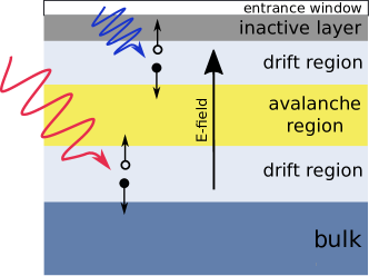
The photon detection efficiency (PDE) is one example where the breakdown probability plays a decisive role. Depending on the photon’s absorption length and the location and extension of the high-field region, a photon is either absorbed before the high-field region (blue photons) or after it (red photons). See Figure 1 for a conceptual sketch of one SiPM cell, which illustrates the situation.
The photon absorption results in the generation of an electron and hole, which - in case the absorption takes place in the active volume of the cell - drift in opposite directions due to the electric field in the depleted volume. If the photon is absorbed after the high-field region in a p-on-n structure like the ones studied here, it is the hole that drifts into the high-field region, if the photon absorbs before the high-field region, it is the electron that drifts down into the avalanche region.
The probability to initiate a Geiger breakdown is smaller for holes than for electrons (due to the lower mobility of holes in silicon, e.g. [13]). If one could measure the probability of a subsequent breakdown as a function of where the electron/hole pair is released one would, therefore, reverse engineer the location and vertical extension of the high-field region. Such a mapping is indeed possible with bias dependent PDE measurements as has been shown in [11, 12].
For the Hamamatsu SiPM we measured the PDE at three wavelengths and for the KETEK device at four wavelengths. A description of the setups and procedures used for the PDE and all other measurements presented here is given in [10].
Like in our previous measurements we find that the PDE for a given wavelength is well fit with the empirical model
| (1) |
where is the relative overvoltage above the breakdown voltage . is the PDE in saturation but is not necessarily the true saturation value because we cannot measure the PDE at higher bias values. The term in square brackets is the breakdown probability, which depends only on the product of the relative overvoltage and a dimensionless parameter , which is mostly dependent on whether an electron or a hole initiates a breakdown as we explain later.222 was jocularly referred to as the Otte number at recent meetings.
In that context it is interesting to remark that empirically all the bias dependent physics of the breakdown is included in one single constant, or in a linear function when larger relative overvoltages than measured here are taken into account [12]. Because our data is well described with one constant we do not need to consider the linear function, which would, furthermore, not be sufficiently constrained by our data. The devices we tested cannot be operated much beyond the measured voltage range.
While the overall fit function is the same as in [12] there are two differences in its usage. Instead of plotting the breakdown probability as a function of absolute bias voltage we use the relative overvoltage . The second difference is that we characterize the electron/hole initiation probability with instead of the voltage at which the PDE reaches 95%. and are inherently less dependent on the structure of the device and temperature than the absolute bias voltage as we shall motivate in the following.
The avalanche and breakdown characteristics of a pn-junction are governed by the ionization rates, which depend strongest on the electric field and much less on device specifics like the doping profile, doping concentrations, or temperature [14]. By parametrizing the breakdown probability as a function of the average electric field in the high-field region and not as a function of absolute voltage one arrives at a parameterization that depends mostly on avalanche physics. With such a parameterization it should then be possible to extract information about the breakdown characteristics that can be compared with measurements from other devices in a meaningful manner.
The bias depends on the device specific parameter , i.e. the effective width of the high field region and thus cannot fulfill the task of a device-independent characterization. The relative overvoltage , on the other hand, is independent of and proportional to .
| (2) |
where is the electrical field at breakdown averaged across the high-field region. We note that drops out if the width of the depleted region does not change between breakdown and operating voltage. That assumption holds true for most available SiPM including the tested devices where the gain as a function of bias voltage is described by a linear function (see Figure 2).
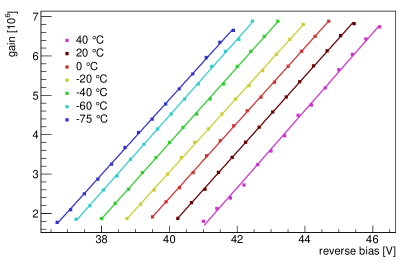
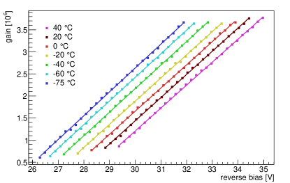
While, as mentioned above, most of the breakdown characteristics depend on the electric field, other factors play a role too. compensates for some but admittedly, not all of the device and temperature dependencies by normalizing to . We can show that at least the temperature dependencies of the breakdown characteristics are properly taken care of. Optical crosstalk measurements taken at 100 K temperature difference fall on top of each other when plotted as a function of (see Figure 5), which would not be the case if plotting against would not compensate for temperature dependencies. The picture is very different when optical crosstalk is plotted as a function of absolute voltage.
Using in the argument of the exponential function of the breakdown probability can be viewed as a Taylor series expansion about the critical electric field . The linear coefficient in the expansion is , the constant term is obviously zero or so small that it is not relevant, higher order terms can be relevant [12]. thus parameterizes the electric field dependence of the breakdown, which as we have discussed above does not depend much on the device specifics. can thus be compared between devices, contrary to the absolute voltage when the breakdown probability reaches 95%.
But the breakdown probability depends strongly on whether an avalanche is initiated by electrons or holes and it is, therefore, expected that changes with changing electron/hole breakdown initiation ratio. Figure 3 shows the breakdown probability derived from the PDE measurements, i.e. the PDE divided by . The solid lines depict the best fit parameterizations of the breakdown probability, which all yield fit probabilities of 30% or better. The fitted values of are listed in Table 1 together with the corresponding photon absorption lengths. The 589 nm light source was not available for the measurement of the Hamamatsu device.
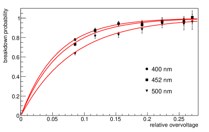
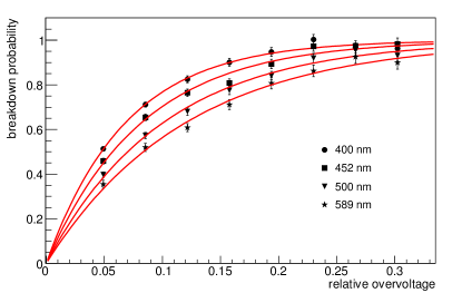
The value of decreases with increasing photon wavelength for each device, which is a testimony to the fact that the breakdown probability shifts from majority electron to majority hole initiated breakdowns. thus shows a clear dependence on the ratio of electron to hole initiated breakdowns.
| Wavelength | Absorp. length | ||
|---|---|---|---|
| nm | m | Hamamatsu | KETEK |
| 400 | 0.082 | ||
| 452 | 0.43 | ||
| 500 | 0.91 | ||
| 589 | 2.0 | N/A | |
The absolute value of should also depend on the dimensions of the avalanche region, which we do not know and thus cannot explore further. For the time being, we resort to the assumption that the dependence of on the width of the avalanche region is small compared to the observed change with photon-wavelength and can be neglected. How valid that assumption is needs to be shown in the future on devices with known dimensions of the high field region. The avalanche regions of the two tested devices probably have fairly similar widths, which we infer from the similarities of their respective breakdown voltages, which are 26.8 V and 37.5 V at 0 ∘C for the KETEK and Hamamatsu SiPM, respectively.
For the Hamamatsu device is 12 for photon absorption lengths of m while the KETEK SiPM yields the same number for absorption lengths of m. If the difference in absorption lengths is taken at face value and does not depend strongly on details of the two structures, it follows that the avalanche region is located m deeper in the Hamamatsu SiPM than in the KETEK SiPM.
Two more observations are that a) in between absorption lengths m and m, changes little in the Hamamatsu SiPM, while it changes much more in the KETEK SiPM. And b) never reaches as high a value in the KETEK SiPM as in the Hamamatsu SiPM. Under the assumption that does not depend strongly on details of the two structures, we interpret both observations as evidence for a location of the avalanche region in the KETEK SiPM that is right below the surface and that already for 400 nm photons a significant fraction of photons absorb after the avalanche region. In the Hamamatsu SiPM, on the other hand, the passive region right below the surface and before the drift volume starts is thinner than in the KETEK device. Thus more photons are absorbed and mostly electrons drift into the high-field region also for nm photons.
In that scenario it is expected that the spectral response of the Hamamatsu device is higher below 400 nm because of the larger active volume above the high field region and thinner passive area. It is also expected that the response of the KETEK SiPM peaks at lower wavelengths than in the Hamamatsu SiPM because the breakdowns change to hole dominate ones for shorter wavelengths in the KETEK device than in the Hamamatsu one. That is indeed what we observe. Figure 4 shows the spectral response of the two devices measured with the setup explained in [10].
4 Where Optical Crosstalk Photons enter a Cell
In this section we discuss how can be used to determine where optical crosstalk photons enter a cell. Optical crosstalk (OC) is caused by photons that are emitted in the breakdown of one cell and propagate into a neighboring cell where they initiate an additional breakdown. One distinguishes two types of OC (see e.g. [15] ) In case the photon absorbs in the active (depleted) volume of a cell, the additional breakdown happens nearly simultaneous to the first breakdown, which is why that type of OC is called prompt or direct OC. If the photon is absorbed in a non-depleted region, e.g. in the bulk, the generated charges first have to diffuse into the depleted volume before they can initiate a breakdown . The diffusion time can take several tens of nanoseconds depending on the distance between the location of the photon absorption and the border to the active volume of the cell; . But it can also be just a fraction of a nanosecond if the photon absorbs close to the border.
How well the two types of OC can be separated depends on how well two subsequent pulses can be separated in the measurement. Any prompt OC measurement is thus always a combination of true prompt OC events and delayed OC events that have a time delay, which is below the capability of the measurement setup to resolve two overlapping pulses. Two pulses can be identified as such in our setup, if they are more than two nanoseconds apart.
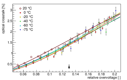
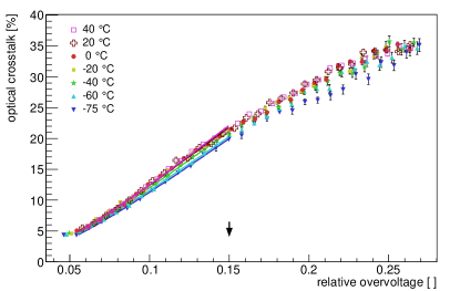
Figure 5 shows the prompt OC of the two devices recorded at seven temperatures between C and C. In this and subsequent measurements, OC is quantified as the probability that the breakdown of one SiPM cell causes one or more other cells to break down too. For the Hamamatsu device we discarded the measurement at C because the contamination from pile-up of uncorrelated dark counts was too large and could not be reliably subtracted. For all other measurements, the accidental pile-up within a 2 ns time window could be subtracted by assuming that the number of dark counts in a given time interval are Poisson distributed. After the correction, all OC curves of one device fall on top of each other, as expected.
We now compare the OC of the two devices at the bias where the breakdown probability for 400 nm photons is 90%.333We do not imply that this operating point is optimal for an application but it allows for an unbiased comparison. The arrow in each panel marks the corresponding relative overvoltage. The KETEK device has a fairly high optical crosstalk of %, which is not surprising because it does not have trenches to prevent photons from propagating into neighboring cells. The prompt OC in the Hamamatsu device, on the other hand, is only 1.5%, which is an impressive improvement compared to past developments [10].
In [10] we showed that a valid model of the optical crosstalk probability vs. relative overvoltage is
| (3) |
where we use from [16] as the number of photons produced per charge carrier in the avalanche that can also cause OC. We note that other measurements of the photon intensity exist, e.g. [17, 18], but those also include spectral components, which are irrelevant for OC, either because the photon absorption lengths are too long (photons do not absorb in the device) or too short (photons absorb in the same cell they are emitted from). is the gain of the SiPM, and is a figure of merit that quantifies what fraction of the photons produced in a breakdown make it into a neighboring cell. The term in square brackets is the breakdown probability already discussed in the previous section.
The OC data in Figure 5 are fit with that model. For the fit we fixed the cell capacitance at 84 fF and 154 fF and the breakdown voltage at 26.8 V and 37.5 V at C, for the KETEK and Hamamatsu SiPM, respectively. The capacitance and breakdown voltages had been measured as described in [10]. The breakdown voltage is found to increase by about 0.1%/∘C in both devices.
The Hamamatsu OC measurements can be fit over the entire measured range with an acceptable fit probability. For the KETEK device, we had to restrict the upper end of the fit range to a relative overvoltage of 0.15, i.e. OC of less than 20%, in order for the fit to yield an acceptable fit probability. It is evident from the KETEK data points, that the OC data turn over in what seems to be a saturating behavior. An explanation for this behavior is that for large OC of more than 20% and the cell size of the device, the probability of more than one OC photon being absorbed in the same cell cannot be neglected anymore. That effect is not included in the fit model.
| Device | Temp. | ||
|---|---|---|---|
| Hamamatsu | -75∘C | 0.0120.001 | 13.91.3 |
| LVR2 | -60∘C | 0.0140.001 | 9.91.4 |
| -40∘C | 0.0130.001 | 10.91.6 | |
| -20∘C | 0.0180.003 | 6.81.2 | |
| 0∘C | 0.0170.001 | 7.20.9 | |
| 20∘C | 0.0140.001 | 160.8 | |
| KETEK | -75∘C | 0.3470.009 | 12.90.7 |
| PM3325 WB | -60∘C | 0.3550.008 | 13.70.8 |
| -40∘C | 0.3780.009 | 13.50.7 | |
| -20∘C | 0.3840.007 | 15.30.7 | |
| 0∘C | 0.420.01 | 12.90.7 | |
| 20∘C | 0.4150.008 | 13.80.6 | |
| 40∘C | 0.4420.007 | 12.80.4 | |
| Hamamatsu LCT5 | 0.0770.001 | 130.2 | |
| SensL J-Series | 0.1260.002 | 8.50.1 | |
| FBK NUV-HD | 0.5570.002 | N/A |
Table 2 lists the values for from the fits. The average values from our previously measured devices are also listed [10]. Comparing the numbers it is evident that the structure of the LVR2 device is 5.5 times better than the LCT5 device in preventing photons from crossing cells. The value for is 0.014, i.e. 1.4% of all photons make it into a neighboring cell where they can cause optical crosstalk. In the KETEK SiPM, between 35% and 44% of the photons cause optical crosstalk.
The second factor that determines the amount of OC is the product of breakdown voltage and cell capacitance, which is 2.25 pFV for the KETEK and 5.78 pFV for the Hamamatsu SiPM. It is a figure of merit that is proportional to the charge generated in an avalanche. Minimizing the figure of merit by designing devices with small breakdown voltage and/or small cell capacitance minimizes OC while retaining good breakdown characteristics, which are governed by .
This time it is the KETEK SiPM that outperforms the Hamamatsu device by a factor of 2.6 because of its smaller cell capacitance. However, the Hamamatsu SiPM has a two times smaller cell capacitance per cell area. We would thus expect that the product of cell capacitance and breakdown voltage for an LVR2 with m cells will be two times lower than for the KETEK device. This assumes that the cell capacitance scales linear with area, which is not necessarily the case as edge effects become important for small cell sizes.
The fit results also allow us to draw conclusions about the location where the crosstalk producing photons are absorbed relative to the avalanche region. For the previously tested Hamamatsu LCT5 SiPM we could show that the majority of these photons are absorbed above the avalanche region [10]. The value we obtained then was . That interpretation was confirmed by Hamamatsu, who found that these photons exit the silicon and reflect off the boundary between the protective layer and the ambient air back into a cell.
In the Hamamatsu SiPM studied here that contribution to the prompt OC has been successfully suppressed by eliminating the protective epoxy layer. The same conclusion comes from the interpretation of . The best fit value for is about in all fits of the optical crosstalk but the one for C, where the fit probability is due to a contamination from random dark counts and can thus be safely ignored (see Table 2). The average value can be compared with the ones we found from the different PDE measurements (Table 1). A small value like 10 corresponds to heavily hole initiated breakdowns, which means that the OC photons must be absorbed below the high-field region. According to Table 1 that is the case if the OC photons absorb in a depth m below the surface.
Three scenarios come to mind that can explain how optical crosstalk photons can be absorbed at such depths. The first scenario is that some photons manage to penetrate the trench between cells. That scenario is unlikely because photons would absorb uniformly across the cell, i.e. absorb above and below the avalanche region and, in consequence, result in values for larger than 10 because the occurring breakdowns would be electron and hole initiated. The second scenario is that some photons with long absorption lengths still bounce off the air-SiPM interface and are absorbed deep inside the device, i.e. mostly below the avalanche structure. The third, and our preferred scenario is that photons cross into a neighboring cell below the trench and are absorbed below the avalanche structure.
In the second and third scenario photons can be absorbed in the bulk and the generated holes diffuse into the active volume where they cause delayed OC (see next section). If the diffusion time is less than 2 ns and thus below the resolving time of our setup, the delayed OC would be misidentified as a prompt OC event. If the photons are absorbed in the active volume below the avalanche region a prompt OC would be caused.
The fit result for the KETEK SiPM yields an number of . Comparing that value with the numbers in Table 1 lets us conclude that the majority of the photons absorb equally distributed across the avalanche region and thus produce an equal amount of electron and hole dominated breakdowns. That result is not surprising as the device does not have trenches in between cells, which would prevent photons to travel directly from the avalanche region where they are produced into a neighboring one.
5 Afterpulsing and Delayed Optical Crosstalk
If the prompt OC in the Hamamatsu device is indeed dominated by misidentified delayed OC, a reduction of the minority carrier lifetimes in the bulk with a low resistivity bulk or a better shielding of the active volume from carriers diffusing out of the bulk with a potential barrier might be a viable way to reduce OC further, unless those measures are already implemented. We illustrate the potential room for improvement by discussing the delayed OC and afterpulsing characteristics of the two tested SiPMs.
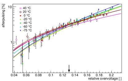
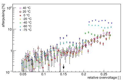
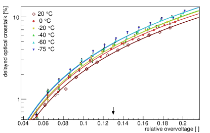
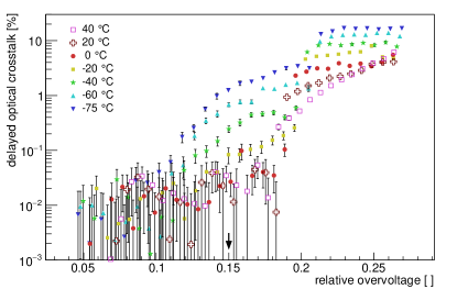
Both quantities are extracted by recording time difference between SiPM pulses as explained in [10]. Afterpulsing events become dominant a few ten nanoseconds after a breakdown when the corresponding cell is recharged to 50% or more of its full capacity. Delayed OC signals dominate at shorter time differences. For the Hamamatsu LVR2 device the subjective division between the two contributions is made at 20 ns, and for the KETEK device at 10 ns. We note that our choice of separating the two contributions in the described way results in a contamination of each measurement with events of the opposite type. That contamination is acceptable for our purposes. Figure 6 shows the afterpulsing and Figure 7 the delayed optical-crosstalk probabilities of both devices.
The KETEK device has an afterpulsing probability of less than 1%, whereas the afterpulsing of the Hamamatsu device is two to three times larger, when compared at their respective bias, which yields a 90% breakdown probability for 400 nm photons (marked by the arrow in the figures). The uncertainties in the different fits of the Hamamatsu afterpulsing data do not allow us to claim a temperature dependence. The afterpulsing of the KETEK SiPM shows irregular behavior for relative overvoltages above 0.2 for the two lowest temperatures. We attribute that behavior to delayed optical crosstalk leaking into the afterpulsing measurement due to our choice of discriminating between the two by means of applying a simple cut in time.
At the same 90% breakdown-probability yielding bias, the delayed OC changes from 0.01% at C to 1% at C for the KETEK SiPM. The temperature dependence is not that strong in the Hamamatsu SiPM, where the delayed OC is 3.5% at C and increases by a factor of 1.3 to 4.5% at C. We discard the delayed OC measurement at C for the same reason we discarded the prompt OC measurement at the same temperature.
Below relative overvoltages of 0.15, afterpulsing and delayed OC of the KETEK device are so low that the measurement is affected by systematic effects. Only at higher overvoltages is it possible to resolve the expected temperature dependence of the delayed optical crosstalk. The dependence is due to an increase of the carrier life times in the bulk with decreasing temperatures.
Comparing the prompt and delayed OC performance of both devices has us speculate about possible future improvements of both technologies. The about ten times lower delayed OC of the KETEK device is an indication that it should be in principle possible to lower the delayed OC in the Hamamatsu technology further. If a lower delayed OC is achieved in the Hamamatsu technology and our assertion that the prompt OC in the present Hamamatsu device is due to misidentified delayed OC events, the effectively measured prompt OC should go down as well. On the other hand, it can be expected that future KETEK developments with trenches will be able to achieve a similar if not better prompt OC performance than observed in the Hamamatsu SiPM.
6 Discussion
In this work we characterized one prototype SiPM from Hamamatsu and the PM3325 WB SiPM from KETEK. Both SiPMs have dramatically improved characteristics when compared to previous devices. The PDE of both devices peaks between 40% and 50% and nuisance parameters are significantly reduced. In particular impressive is the 1.5% prompt optical crosstalk of the Hamamatsu device, which is four times lower than in the Hamamatsu LCT5 device [10]. Equally impressive are the low afterpulsing and delayed optical crosstalk of the KETEK device, which are both less than 1%. A device that combines the excellent features of both SiPMs would result in another significant improvement in the SiPM technology.
Analysis methods that probe the microphysics of SiPMs help to understand how SiPMs work and ultimately provide input in the design of future SiPM developments. For that purpose we discussed how the vertical structure of the high-field region is mapped with bias dependent breakdown probability measurements and how such a mapping can be utilized to learn about the origin of charge carriers relative to the avalanche structure. Using the method we could show that the prompt OC producing photons in the Hamamatsu SiPM must be absorbed below the avalanche structure contrary to the LCT5 device where the majority of OC photons enter the avalanche region from the surface side. In the KETEK device, the optical-crosstalk photons illuminate the avalanche region of a neighboring cell from the side. This information will help to further improve the prompt OC performance in future devices. We are not aware of another experimental method that provides the same information.
The -method could also be used to identify the spatial origin of charge carriers produced by delayed optical crosstalk, afterpulsing, and dark counts relative to the avalanche region. However, two requirements need to be fulfilled first. A valid model has to exist that properly describes the bias dependence of the characteristic of interest and includes the breakdown probability. And the measurement cannot be contaminated, like, for example, our delayed optical crosstalk measurement, which also includes some afterpulsing events. Unless, of course, the model takes these contaminations into account too.
The empirical mapping of the values obtained in PDE measurements to the photon absorption length allowed us to determine how far below the surface the avalanche region is located. However, because we have no access to the structure of the studied devices, we cannot verify the absolute accuracy of the mapping and the dependence of on the size of the avalanche region. To verify that assumption and for a more precise probing of the high-field structure, dedicated test structures are needed for calibration. The main parameters to vary in these structures are the size of the region and its location below the surface.
Analytical modeling that links to the microphysics of the breakdown, like the ionization coefficients and the electron/hole breakdown initiation ratio, would further improve the understanding of SiPMs and expand the usability of the method. We hope that this paper inspires future work in that direction.
Acknowledgment
We are grateful to Hamamatsu and KETEK, who have provided us with samples of their latest developments. This research was in part supported by the National Science Foundation under grant no. PHYS-1505228.
References
-
[1]
S. Ogawa,
Liquid
xenon calorimeter for MEG II experiment with VUV-sensitive MPPCs, Nuclear
Instruments and Methods in Physics Research Section A: Accelerators,
Spectrometers, Detectors and Associated Equipment 845 (2017) 528–532.
doi:10.1016/J.NIMA.2016.06.085.
URL http://www.sciencedirect.com/science/article/pii/S0168900216306489 -
[2]
F. Moreau, J. C. Vanel, O. Drapier, M. Gonin, A. Bonnemaison, A. Cauchois,
Y. Geerebaert, S. Couturier-Le Quellec,
Mass
characterization of multi-pixel photon counters for the T2K 280 m near
detector, Nuclear Instruments and Methods in Physics Research, Section A:
Accelerators, Spectrometers, Detectors and Associated Equipment 613 (1)
(2010) 46–53.
doi:10.1016/j.nima.2009.11.042.
URL http://www.sciencedirect.com/science/article/pii/S0168900209022220 -
[3]
E. J. Mannel, An SiPM
based readout for the sPHENIX calorimeters, in: IEEE Nuclear Science
Symposium Conference Record, IEEE, 2013, pp. 1–4.
doi:10.1109/NSSMIC.2013.6829439.
URL http://ieeexplore.ieee.org/document/6829439/ -
[4]
H. Anderhub, M. Backes, A. Biland, V. Boccone, I. Braun, T. Bretz, J. Buß,
F. Cadoux, V. Commichau, L. Djambazov, D. Dorner, S. Einecke, D. Eisenacher,
A. Gendotti, O. Grimm, H. Von Gunten, C. Haller, D. Hildebrand,
U. Horisberger, B. Huber, K. S. Kim, M. L. Knoetig, J. H. Köhne,
T. Krähenbühl, B. Krumm, M. Lee, E. Lorenz, W. Lustermann, E. Lyard,
K. Mannheim, M. Meharga, K. Meier, T. Montaruli, D. Neise, F. Nessi-Tedaldi,
A. K. Overkemping, A. Paravac, F. Pauss, D. Renker, W. Rhode, M. Ribordy,
U. Röser, J. P. Stucki, J. Schneider, T. Steinbring, F. Temme, J. Thaele,
S. Tobler, G. Viertel, P. Vogler, R. Walter, K. Warda, Q. Weitzel,
M. Zünglein,
Design
and operation of FACT-the first G-APD Cherenkov telescope, Journal of
Instrumentation 8 (6) (2013) P06008–P06008.
doi:10.1088/1748-0221/8/06/P06008.
URL http://stacks.iop.org/1748-0221/8/i=06/a=P06008?key=crossref.215223ca70483ee275407a04fbb44da8 - [5] A. Otte, K. Meagher, T. Nguyen, M. Carroll, S. Hooper, K. Mckinney, S. Peet, Silicon photomultiplier integration in the camera of the mid-size Schwarzschild-Couder Cherenkov telescope for CTA, Nuclear Instruments and Methods in Physics Research, Section A: Accelerators, Spectrometers, Detectors and Associated Equipment 787 (2015) 85–88. doi:10.1016/j.nima.2014.11.026.
- [6] A. N. Otte, J. Barral, B. Dolgoshein, J. Hose, S. Klemin, E. Lorenz, R. Mirzoyan, E. Popova, M. Teshima, A test of silicon photomultipliers as readout for PET, Nuclear Instruments and Methods in Physics Research, Section A: Accelerators, Spectrometers, Detectors and Associated Equipment 545 (3) (2005) 705–715. doi:10.1016/j.nima.2005.02.014.
-
[7]
V. C. Spanoudaki, A. B. Mann, A. N. Otte, I. Konorov, I. Torres-Espallardo,
S. Paul, S. I. Ziegler,
Use
of single photon counting detector arrays in combined PET/MR:
Characterization of LYSO-SiPM detector modules and comparison with a LSO-APD
detector, Journal of Instrumentation 2 (12) (2007) P12002–P12002.
doi:10.1088/1748-0221/2/12/P12002.
URL http://stacks.iop.org/1748-0221/2/i=12/a=P12002?key=crossref.e10b977bd4b95190897aebb2163f748f -
[8]
M. Perenzoni, D. Perenzoni, D. Stoppa,
A 64 x 64-Pixels
Digital Silicon Photomultiplier Direct TOF Sensor With 100-MPhotons/s/pixel
Background Rejection and Imaging/Altimeter Mode With 0.14% Precision Up To
6 km for Spacecraft Navigation and Landing, IEEE Journal of Solid-State
Circuits 52 (1) (2017) 151–160.
doi:10.1109/JSSC.2016.2623635.
URL http://ieeexplore.ieee.org/document/7756659/ - [9] R. Agishev, A. Comerón, J. Bach, A. Rodriguez, M. Sicard, J. Riu, S. Royo, Lidar with SiPM: Some capabilities and limitations in real environment, Optics and Laser Technology 49 (2013) 86–90. doi:10.1016/j.optlastec.2012.12.024.
-
[10]
A. N. Otte, D. Garcia, T. Nguyen, D. Purushotham,
Characterization of Three High
Efficiency and Blue Sensitive Silicon Photomultipliers, Nuclear Instruments
and Methods in Physics Research Section A: Accelerators, Spectrometers,
Detectors and Associated Equipment 14 (8) (2016) 1–21.
arXiv:1606.05186,
doi:http://dx.doi.org/10.1016/j.nima.2016.09.053.
URL http://arxiv.org/abs/1606.05186 -
[11]
A. N. Otte,
SiPM’s
a very brief review, in: International Conference on New Photo-Detectors,
Moscow, 2015.
URL http://indico.inr.ru/event/4/session/1/contribution/81/material/slides/0.pdf -
[12]
G. Zappalà, F. Acerbi, A. Ferri, A. Gola, G. Paternoster, V. Regazzoni,
N. Zorzi, C. Piemonte,
Study
of the photo-detection efficiency of FBK High-Density silicon
photomultipliers, Journal of Instrumentation 11 (11) (2016) P11010–P11010.
doi:10.1088/1748-0221/11/11/P11010.
URL http://stacks.iop.org/1748-0221/11/i=11/a=P11010?key=crossref.b0de4efb86f2d245334693c679c4f821 -
[13]
W. G. Oldham, R. R. Samuelson, P. Antognetti,
Triggering Phenomena in
Avalanche Diodes, IEEE Transactions on Electron Devices 19 (9) (1972)
1056–1060.
doi:10.1109/T-ED.1972.17544.
URL http://ieeexplore.ieee.org/document/1477015/ - [14] S. M. Sze, K. K. Ng, Physics of semiconductor devices, Wiley-Interscience, 2007.
-
[15]
P. Buzhan, B. Dolgoshein, A. Ilyin, V. Kaplin, S. Klemin, R. Mirzoyan,
E. Popova, M. Teshima,
The
cross-talk problem in SiPMs and their use as light sensors for imaging
atmospheric Cherenkov telescopes, Nuclear Instruments and Methods in
Physics Research, Section A: Accelerators, Spectrometers, Detectors and
Associated Equipment 610 (1) (2009) 131–134.
doi:10.1016/j.nima.2009.05.150.
URL https://www.sciencedirect.com/science/article/pii/S0168900209010456 -
[16]
A. Nepomuk Otte,
On
the efficiency of photon emission during electrical breakdown in silicon,
Nuclear Instruments and Methods in Physics Research, Section A: Accelerators,
Spectrometers, Detectors and Associated Equipment 610 (1) (2009) 105–109.
doi:10.1016/j.nima.2009.05.085.
URL https://www.sciencedirect.com/science/article/pii/S0168900209010390 -
[17]
A. Lacaita, M. Ghioni, F. Zappa, G. Ripamonti, S. Cova,
Recent
advances in the detection of optical photons with silicon photodiodes,
Nuclear Inst. and Methods in Physics Research, A 326 (1-2) (1993) 290–294.
doi:10.1016/0168-9002(93)90366-P.
URL http://linkinghub.elsevier.com/retrieve/pii/016890029390366P -
[18]
R. Mirzoyan, R. Kosyra, H. G. Moser,
Light
emission in Si avalanches, Nuclear Instruments and Methods in Physics
Research, Section A: Accelerators, Spectrometers, Detectors and Associated
Equipment 610 (1) (2009) 98–100.
doi:10.1016/j.nima.2009.05.081.
URL https://www.sciencedirect.com/science/article/pii/S0168900209010377