nEXO Collaboration
Imaging individual barium atoms in solid xenon for barium tagging in nEXO
Abstract
The search for neutrinoless double beta decay probes the fundamental properties of neutrinos, including whether or not the neutrino and antineutrino are distinct. Double beta detectors are large and expensive, so background reduction is essential for extracting the highest sensitivity. The identification, or “tagging”, of the 136Ba daughter atom from double beta decay of 136Xe provides a technique for eliminating backgrounds in the nEXO neutrinoless double beta decay experiment. The tagging scheme studied in this work utilizes a cryogenic probe to trap the barium atom in solid xenon, where the barium atom is tagged via fluorescence imaging in the solid xenon matrix. Here we demonstrate imaging and counting of individual atoms of barium in solid xenon by scanning a focused laser across a solid xenon matrix deposited on a sapphire window. When the laser sits on an individual atom, the fluorescence persists for 30 s before dropping abruptly to the background level, a clear confirmation of one-atom imaging. No barium fluorescence persists following evaporation of a barium deposit to a limit of 0.16%. This is the first time that single atoms have been imaged in solid noble element. It establishes the basic principle of a barium tagging technique for nEXO.
pacs:
32.30.-r,32.50.+d,32.90.+a,14.60.Pq,23.40.-sThe search for neutrinoless double beta decay () is an important probe into the nature of neutrinos. Observation would imply that neutrinos are Majorana particles, would demonstrate violation of lepton number conservation, and could help determine the absolute neutrino mass1. EXO-200 is searching for in 136Xe with 110 kg of active liquid Xe (LXe) enriched to 80.6 136Xe in a time projection chamber (TPC). Two-neutrino double beta decay () of 136Xe has been observed in EXO-200, and its half-life is measured at (stat)(sys) yr EXO200TwoNuLong . The most recent EXO-200 search sets a limit on the half-life at > 1.81025 yr (90 CL), which corresponds to an effective Majorana neutrino mass of < 147-398 , depending on nuclear matrix element calculations EXO200ZeroNuPRL .
A 136Xe TPC provides a unique opportunity to tag the daughter 136Ba at the site of a double beta decay event. The implementation of this barium tagging would improve sensitivity by effectively eliminating all backgrounds except Moe1991 . Barium tagging is being investigated for a future upgrade of the next-generation LXe experiment, nEXO, a 5 tonne enriched Xe experiment recently described in pCDR ; sensitivity . Initial results have been reported for research on methods of barium tagging in LXe Mong2015 ; Twelker2014 , and also in a Xe gas TPC Brunner2015 . The NEXT collaboration has recently reported images of single Ba++ in fluorescent dye molecules from a dilute deposit of barium perchlorate salt solution NEXTPRL .
This paper presents a major step towards realization of barium tagging in solid Xe (SXe) for nEXO Mong2015 . In this method, a cryogenic probe would be moved to the position of the candidate event in LXe, and the daughter atom or ion would be captured in a small amount of SXe on a sapphire window at the end of the probe Wamba ; Rowson . It would then be detected by its laser-induced fluorescence in the SXe. It is expected that a Ba++ ion will convert to Ba+ in LXe, as the LXe conduction band gap is less than the ionization potential for Ba+ Moe1991 . Neutralization to barium may also occur in the charge cloud following a event. A study of 214Bi daughters of 214Pb -decay in EXO-200 has reported that 76(6) of these daughters are ionized, with negligible subsequent neutralization after many minutes alphaion . Thus, a large fraction of 136Ba daughters is expected to be in the singly ionized state in LXe. Whether or not the 136Ba will remain ionized in SXe on a cold probe is not yet known.
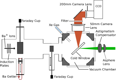
Significant progress on understanding the spectroscopy of Ba in SXe has been made Mong2015 ; McCaffrey2016 ; McCaffrey2018 . Through theoretical modeling, the strongest fluorescence peaks at 577 and 591 are identified as barium atoms in 5-atom and 4-atom vacancy sites in the SXe matrix McCaffrey2018 . These two fluorescence peaks bleach fairly rapidly at high laser intensity, e.g. using a focused laser beam Mong2015 . Obtaining large numbers of photons from single barium atoms in these matrix sites would benefit from a method to overcome bleaching, e.g., with repumping lasers. The barium emission peak at 619 , although not reported in some deposits made at 10 McCaffrey2016 ; McCaffrey2018 , is more prominent in annealed deposits or deposits made at higher temperature and observed at 10 Mong2015 ; McCaffrey-pc . The 619 peak is attributed in this work to barium atoms in a single vacancy (SV) site. This peak exhibits less bleaching than the 577 and 591 emission peaks and thus is more amenable to single barium atom imaging. The apparatus for depositing and observing Ba/Ba+ deposits in SXe is described in Mong2015 . Important components are shown in Fig. 1.
In this work, imaging of single barium atoms in SXe via the 619 fluorescence peak is reported. This is the first time that single atoms have been imaged in a solid noble element matrix. Images of single DBATT dye molecules in solid krypton and xenon Sepiol as well as Mg-TAP molecules in solid xenon Starukhin have been obtained previously.
I Results
I.1 Fixed Laser Images
The barium fluorescence in a given deposit is determined by summing the counts in a 44 pixel area enclosing the laser spot and subtracting the SXe-only background. The background is measured by averaging the summed CCD counts in the focused laser region from the prior and following SXe-only deposits for each Ba+ deposit. A typical background level is 1000 . The observed barium counts per mWs of laser exposure vs. Ba+ ions deposited in the laser region are plotted in Fig. 2(a). Since the neutralization fraction is not known, the number of barium atoms in the laser beam is less than or equal to the number of ions deposited. Each point represents a separate Ba+ deposit with the signal averaged over 4 laser positions separated by 20 on the deposit. The error bar is the standard deviation of the four measurements. The observed signal is linear with a log-log slope of . The slope of the linear fit is per ion. Including the uncertainty in number of ions deposited, the observed fluorescence per ion is 379 per ion. For these measurements, 40 of focused 572 laser excitation was used with 3 of laser exposure.
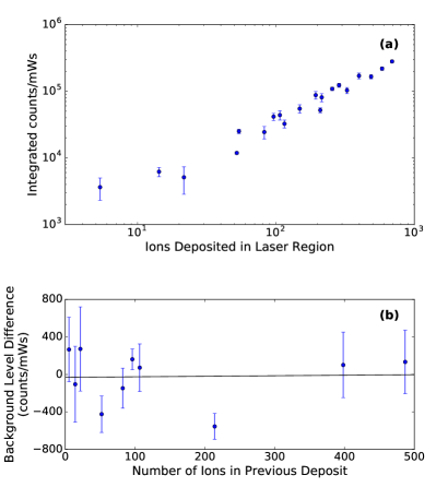
For a practical barium tagging application in nEXO, it is crucial for each barium tag to be independent of any previous tagging measurements or residual barium on the cryogenic probe to ensure that the barium daughter is correlated to the decay candidate being investigated. To obtain a quantified limit of this “erasure” property, the difference in the background level of the last SXe-only deposit before and the SXe-only immediately after a barium deposit in Fig. 2(a) is plotted in Fig. 2(b). The data are averaged over four laser positions for each deposit, and the standard deviation is shown as an error bar. The differences are consistent with zero, and the slope of a linear fit, per ion is a measure of the barium signal remaining after evaporation. The ratio of the maximum value of the SXe-only difference fit to the minimum barium signal response from the slope of Fig. 2(a) gives a limit of 0.16% on residual barium fluorescence after evaporation.
I.2 Scanned Images
By further decreasing the density of barium ions deposited, single barium atoms can be spatially resolved. To image these atoms, the laser is rastered across the deposit. A typical scan consists of laser displacements in a square grid of 1212 steps with 3 of laser exposure and a spacing of 4 . The raw CCD images of four successive steps of a laser scan are shown in Fig. 3. As the laser passes over the barium atom, a strong 619 signal appears. When the laser moves off of the barium atom, the observed counts return to background level.

A scan image of this region is generated by integrating the CCD counts in a 44 pixel area encompassing the laser region in each frame. These integrals are divided by the laser exposure, and arranged according to the position of each spot in the grid. Five such scan images, taken from a typical experiment, are shown in Fig. 4. Data from the four frames shown in Fig 3 contribute to four points in line y=7 in Fig. 4(b). In the first SXe-only deposit, no fluorescence peaks are found in the scan (Fig. 4(a)). After this, the deposit is evaporated by heating the sapphire window to 100 . Then, a new SXe deposit with 12 pulses of the Ba+ ion source, corresponding to 48 Ba+ ions in the full scan area is produced. Two large peaks of roughly equal size in an otherwise low-background area are observed in a scan of this deposit (Fig. 4(b)). This distinguishes each peak as the location of a single resonant barium atom. This scan is then repeated, and the barium peaks persist, as seen in Fig. 4(c).
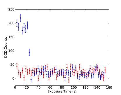
At this point, the laser is moved to the location (x,y)=(4.75,6.00), and many 3 exposures are taken. Although not intended, this position is not the same as the peak frame (4,7) but is close to the position of frame (5,6). The time dependence of the integrated signal from a 33 pixel area of the single barium peak is shown in Fig. 5. The average signal level of 192 counts agrees with the single barium values at this position in the scans, 184 and 169 counts, respectively, taking into account 33 rather than 44 pixel integration. This signal persists for 30s of laser exposure, including the prior two scans, before abruptly dropping to the average background level of 21 counts. This discrete turn-off of the fluorescence signal is a hallmark of a single atom.
About 3300 photons (0.5 CCD ) are detected from this atom. This corresponds to around 1.4106 photons absorbed and emitted by one atom. For comparison, the standard deviation of the SXe-only background at one laser position in Fig. 5 for a 30 integration is 47 detected photons. Thus, the single barium atom fluorescence signal is 70 above background fluctuations at one laser position. For different laser positions in the SXe-only scans, Fig. 4 (a) and (e), the background fluctuation is 30 detected photons in a 3 integration. Comparing this to 330 barium atom fluorescence photons in 3, the barium peaks in a composite image, such as those in Fig. 4 (b-d), are 11 above background.
Following this fixed laser position run, a third scan is done, and the barium peak on the left has disappeared, as expected. The right barium peak on the edge of the scan persists, as seen in Fig.4 (d). After evaporating this deposit, a new SXe-only deposit is made. As in the previous SXe-only deposit, no peaks are observed in this scan (Fig.4 (e)). This illustrates the lack of any “history effect” due to previous barium deposits and the absence of any signal from possible barium contamination on the sapphire window.

II Discussion
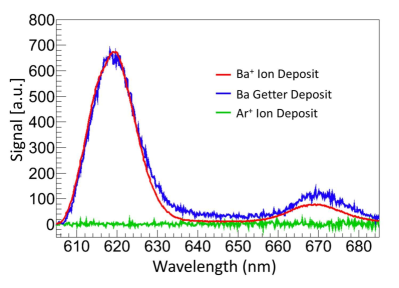
The barium sample in this work is deposited as Ba+ ions. The fluorescence lines of Ba+ in SXe are expected in the blue-green region rather than the yellow-red region. Thus a spectroscopic assignment of the 619 emission line to barium rather then Ba+ is favored. To further test this, a spectrum of a neutral barium deposit made with the barium getter source is compared in Fig. 6 to a spectrum of a Ba+ deposit. Identical spectra are observed using the two sources under similar conditions. This confirms the 619 emission line as associated with barium atoms resulting from neutralization of the incident Ba+ ions. In addition, no fluorescence peak is observed from deposits of Ar+ ions in SXe at 2000 under similar conditions. This rules out matrix damage as the source of the 619 peak.
A reasonable assignment of the 619 nm emission is to barium atoms in a single vacancy (SV) site. The previously studied case of Na+ in solid argon (SAr) matrix is a good analogy. A higher fraction of Na atoms was found in SV sites with Na+ ions incident from a laser ablation or ion beam source than with Na atoms from a thermal atom source Tam-Fajardo ; Silverman-Fajardo ; Vaskonen ; Ahokas . In the model presented in Silverman-Fajardo , Na+ ions preferentially form in SV sites in SAr due to tighter ion binding. Subsequently, some ions are neutralized, resulting in Na atoms in cramped SV sites. Similarly, a barium ion with Ba+Xe equilibrium radius of 3.619 Buchachenko should prefer an SV site of 4.39 radius in SXe at 50 Granfors rather than a larger multivacancy site. After neutralization from Ba+ to Ba, the barium atom with BaXe equilibrium radius of 5.5 Buchachenko ; McCaffrey2016 ; McCaffrey2018 is cramped in the SV site, but creation of additional vacancies may not be energetically favorable. In the following paragraphs, alternate barium molecule interpretations are considered, and found to be inconsistent with observations.
Assignment to Ba2 is unlikely as a linear relationship of signal vs. ions deposited is observed in Fig. 2(a), rather than quadratic. At the low ion density of Fig. 4, implanted Ba+ ions are separated, on average, by 8 . Since the Ba+ ions are implanted 7 5 SRIM below the surface of the SXe, mobility of the neutralized barium atoms should be limited.
Reactions of deposited Ba with residual gas impurities, such as water and oxygen to form molecules should also be considered. A limit of < 100 residual gas molecules in the SXe matrix is established through fringe rate and partial pressure comparisons. The most likely species to form are BaOH and BaO, through the reactions
| (1) |
Both processes are endothermic Murad1981 , and thus energetically unfavored. BaOH vapor has known emission bands in the green at 487 and 512 , and in the IR at 712-758 and 783-839 BaOHlines . These do not agree with the observed 619 emission. At low temperature, the upper state of BaO should be primarily the A() state. This state has a multi-line spectrum in vacuum with calculated values from 455 - 865 BaOlines . The =0 to =2 and 4 transitions are close to our observed peaks at 619 nm and 670 , but adjacent transitions are missing. Furthermore, the excitation spectra of these peaks are different, contradicting a common =0 upper state for the emission. The A state lifetime of 356 in vacuum Johnson1972 , is discrepant with the 7 decay lifetime of the observed 619 emission line presented in this work. Thus, this line is not due to BaO.
III Conclusions
The imaging and counting of individual barium atoms with high definition in solid xenon by scanning a focused laser has been demonstrated. The 619 emission peak observed in deposits of Ba+ and Ba in solid xenon is attributed to neutral barium atoms in a single-vacancy substitution site. The observation of two isolated peaks in a scan with roughly equal size fluorescence in an otherwise low-background area clearly distinguishes each peak as the location of an individual resonant barium atom. With prolonged laser exposure, the sudden, discrete turn-off of the fluorescence, with signal dropping to background level, is strong confirming evidence that the fluorescence is from one atom only. This is the first imaging of individual atoms in a solid rare element. Additional unique features of this work are very low background obtained by pre-bleaching the substrate and a demonstrated limit of 0.16% for “erasure” of barium signal by deposit evaporation. Successful counting of individual barium atoms in solid xenon is a significant step toward barium tagging in the nEXO neutrinoless double beta decay experiment.
Acknowledgements
The authors are grateful to Picoquant for the loan of the time resolved photon counting equipment. Valuable discussions with J. G. McCaffrey, B. Gervais and A. van Orden are appreciated. This material is based upon work supported by the National Science Foundation under Grant Number PHY-1649324 and the U.S. Department of Energy, Office of Science, Office of High Energy Physics under Award Number DE-FG02-03ER41255.
References
- (1) M. Tanabashi et al. (Particle Data Group), Phys. Rev. D 98, 030001 (2018) (http://pdg.lbl.gov).
- (2) J. Albert et al. (EXO-200 Collaboration), Phys. Rev. C 89, 015502 (2014).
- (3) J. Albert et al. (EXO-200 Collaboration), Phys.Rev.Lett. 120, 072701 (2018).
- (4) M. Moe, Phys. Rev. C 44, R931 (1991).
- (5) S. Al Kharusi et al. (nEXO Collaboration), arXiv:1805.11142 [physics.ins-det] (2018).
- (6) J. Albert et al. (nEXO Collaboration), Phys. Rev. C 97, 065503 (2018).
- (7) B. Mong et al., Phys. Rev. A 91, 022505 (2015).
- (8) K. Twelker et al., Review of Scientific Instruments 85, 095114 (2014).
- (9) T. Brunner et al., International Journal of Mass Spectrometry 379, 110-120 (2015).
- (10) A.D. McDonald et al. (NEXT Collaboration), Phys.Rev.Lett. 120, 132504 (2018).
- (11) K. Wamba, (PhD Dissertation), Stanford University, (2006).
- (12) P.C. Rowson, Stanford Linear Accelerator Center, Cryogenic Ion Capture Probe R&D at SLAC, SLAC-PUB-17110, (2017).
- (13) J. Albert et al. (EXO-200 Collaboration), Phys. Rev. C 92, 045504 (2015).
- (14) B.M. Davis, J.G. McCaffrey, J. Chem. Phys. 144, 1044308 (2016); doi: 10.1063/1.4940688
- (15) B.M. Davis, B. Gervais, J.G. McCaffrey, J. Chem. Phys. 148, 124308 (2018); doi: 10.1063/1.5019890
- (16) The 619 nm emission peak has been observed in higher temperature deposits by the McCaffrey group (J. G. McCaffrey private communication).
- (17) J. Sepiol et. al., Chem. Phys. Lett. 311, (1999); doi: 10.1016/S0009-2614(99)00753-8
- (18) A. Starukhin et. al., Chem. Phys. 285, (2002); doi: 10.1016/S0301-0104(02)00694-8
- (19) S. Tam and M.E. Fajardo, J. Chem. Phys. 99, 854 (1993); doi: 10.1063/1.465348
- (20) D.C. Silverman and M.E. Fajardo, J. Chem. Phys. 106, 8964 (1998); doi: 10.1063/1.474029
- (21) K. Vaskonen, J. Eloranta, and H. Kunttu Chem. Phys. Lett. 310, 245 (1999); doi: 10.1016/S0009-2614(99)00694-6
- (22) J. Ahokas, T. Kiljunen, J. Eloranta, and H. Kunttu J. Chem. Phys. 112, 2420 (2000); doi: 10.1063/1.480825
- (23) A.A. Buchachenko and L.A. Viehland, J. Chem. Phys. 148, 154304 (2018); doi: 10.1063/1.5025861
- (24) P.R. Granfors, A.T. Macrander, and R.O. Simmons Phys. Rev. B 24, 4753 (1981).
- (25) J.F. Ziegler, M.D. Ziegler, J.P. Biersack, SRIM- the stopping and range of ions in matter. Nucl. Instr. Meth. Phys. Res. B, 268, (2010)
- (26) E. Murad, J. Chem. Phys. 75, 4080 (1981); doi: 10.1063/1.442567
- (27) M. Charton and A.G. Gaydon, Proc. Phys. Soc. A 69, 520 (1956)
- (28) K. Sakurai, S.E. Johnson, and H.P. Broida, J. Chem. Phys. 52, 1625 (1970); doi: 10.1063/1.1673196
- (29) S.E. Johnson, J. Chem. Phys. 56, 149 (1972); doi: 10.1063/1.1676841
Methods
Ba/SXe Sample Deposition. The source of barium is an ion beam at 2 keV energy, filtered to select Ba+ with an EB velocity filter. A set of pulsing plates produces 1 s ion bunches for depositing small numbers of ions. The spectra of Ba+ ion deposits in the SXe matrix exhibit peaks known to be due to neutral Ba atoms [7]. Thus some percentage of the ions neutralize in the matrix, although the fraction has not yet been determined. An alternative source of neutral Ba is a BaAl4 getter wire which can be moved into the beam path and heated to emit barium atoms toward the sample. However, it is challenging to achieve low barium flux with this source and to calibrate it.
Deposits are made on a cold sapphire window tilted at 45 with respect to the Ba+ beam. To create a sample, Xe gas is directed toward the window by opening a leak valve. The Xe gas freezes onto the window and forms a SXe matrix with a thickness of around a micron. This is initiated a few seconds prior to the barium deposit, continues during the barium deposit, and is turned off a few seconds after the barium deposit by closing the valve. Thus, the barium atoms are located sparsely in a thin layer at about half the depth of the SXe.
In this work, deposition is done with the sapphire window at a temperature of 50 K. This reduces hydrogen, nitrogen and oxygen content in the matrix, as these residual gases condense below 50 K in vacuum [7]. The window is then cooled to 11 K for observation. Xe is deposited at a rate of around 60 nm/s. An experiment cycle consists of a deposit at 50 K, a fluorescence observation at 11 K, and then evaporation of the deposit by heating the window to 100 K. Many deposits are made in a day with varying numbers of ions deposited, as well as periodic SXe-only deposits to establish the background.
Measurement of Ba ion density. The area density of deposited Ba+ ions cannot be measured directly because the window is an insulator. During the deposit, only the induction signal of the pulse of ions in transit through a circular induction plate is recorded. To estimate the deposited ion density, the pulsed ion beam is sampled before and after deposits by two Faraday cups located 17.5 cm and 4.5 cm before the window. The factor for conversion of these signals to ion density on the window is measured in a separate calibration procedure in which the window is replaced by a third Faraday cup at the window position, and the alignment and magnitude of the three cup signals are compared under conditions similar to that of actual deposits. The uncertainty in the Faraday cup measurements is estimated as -10% due to secondary electron effects, measured by biasing the Faraday cup electrodes. An additional +0% to -10% uncertainty in the ion density deposited on the observation window is included for possible 1 mm misalignment of the approximately Gaussian ion beam, with a full width at half maximum of 5.1 mm, relative to the excitation laser. Conservatively adding these two uncertainties linearly, the total uncertainty in barium ion density at the window is +10% to -20%.
The number of Ba+ ions deposited within the 1/e radius of the laser beam gives a rough upper limit to the number of barium atoms responsible for the observed signal with a fixed laser beam. For typical ion bunch densities of 0.1-1 fC/mm2 and focused laser 1/e radii of w0x = 3.2 m and w0y = 3.8 m, this results in about 0.001-0.01 Ba+ ions/pulse in the 1/e intensity laser region.
Excitation laser system. The excitation laser, a Coherent 599 cw dye laser with Rhodamine 6G dye, pumped by the 532 nm line of a Coherent Verdi-V8 laser, enters from the back side of the window. To position the laser beam with sub-m precision, two computer controlled piezoelectric translation stages are used to move the laser focusing lens. Barium fluorescence light is collected and collimated by a 50 mm Nikon camera lens. A filter with a sharp-edged band-pass of 610-630 nm passes just the 619 nm fluorescence peak. A 200 mm Nikon camera lens then focuses the light onto a liquid nitrogen cooled CCD [31], resulting in an image of magnification. Each of the 2020 m pixels of the CCD represents approximately a 57 m area on the SXe sample, which is at tilted at 45 in the y-direction.
For a given laser intensity, the smallest focus possible is desired for optimal signal-to-background ratio from single atoms. To achieve this, an aspherical lens of 7.9 cm focal length [32] is used to minimize spherical aberration, and a fused silica optical flat of 1 cm thickness is placed at 9 after the lens in order to compensate for astigmatism caused by the tilted sapphire window.
Vibrations of the sapphire window relative to the excitation laser increase the area of laser exposure, and reduce the average intensity seen by a single barium atom. The main source of vibration is the cryostat He compressor cycle, which pulses with a frequency of about 2.25 Hz. To limit the laser exposure to a segment of the cryostat cycle with minimal vibration, a shutter is placed in the laser path and synchronized with the signal from an accelerometer on the outside of the cryostat. This laser gating has 45% duty cycle.
Backgrounds for 619 nm emission. A typical CCD image recorded with a focused laser beam at 570 nm is shown in Extended Data Fig. 1. A strong signal from the barium deposit in SXe on the front surface of the window is visible. A Gaussian fit to the image gives a 1/e2 radius of 10.4 m, which is larger than the average laser beam radius of w = 3.5 m. Aberrations and vibrations in the collection optics and imperfections in the surface of the SXe layer contribute to blurring of the image. A weak background emission from the opposite window surface is also visible.
Very low concentrations of Cr3+ in the sapphire bulk (sub-ppb level) produce a sharp fluorescence peak at 693 nm, with a broad tail extending to the 610-630 nm region passed by the band-pass filter. This results in the faintly visible line through the window in the CCD image. Commercially available c-plane quality sapphire from Meller Optics and Rubicon Technologies has been found to have sufficiently low Cr3+ concentrations for detecting single barium atoms.
The background emission from the front sapphire surface beneath the SXe layer is the main challenge for single barium imaging. It has been found that this background can be reduced significantly and semi-permanently by photo-bleaching. A variety of wavelengths have been used effectively for bleaching, including 514.5 nm, 532 nm, 570-572 nm, and 580.5 nm. A typical bleaching procedure consists of a repeating raster scan of an 80 mW 532 nm laser, focused to around w0 = 10 m, in a 1414 position grid, with 8 m grid spacing and 20 m at each position per scan. This is done with the sapphire window at 100 K. As seen in a subsequent imaging scan in Extended Data Fig. 2, this reduces the surface background 30 over a region of about 9090 m. This area is large enough to accommodate both the fixed laser and scanned images presented in Sec. I.2 in the main article text.
Time resolved photon counting. The decay lifetimes of both the sapphire surface background and the average signal from many barium atoms were investigated using a 561 nm pulsed laser with 100 ps pulse length as the excitation source, and a single photon avalanche photodiode (SPAD) as the detector. The time between the laser pulse and the arrival of a photon at the SPAD was measured by a fast counter, and a histogram of photon arrival times was recorded [33]. The decay histograms for a SXe-only (green) and Ba in SXe (blue) deposit, are shown in Extended Data Fig. 3. By subtracting the SXe-only histogram from the barium histogram, the decay lifetime for the 619 nm emission of barium was isolated and measured to be 7.0 0.3 ns. The SXe-only background decay is comprised of more than one decay constant, but is nonetheless significantly shorter than the barium decay lifetime. By time gating the CCD or SPAD, the signal to background ratio can be increased by a factor of 2 with a loss of 50% of the barium signal. In the future, a sapphire window will be mounted at the end of a cryoprobe Mong2015 , likely to be made of some type of metal. Background emission from the metal tubing may be a concern for barium atom detection. The observed lifetime of emission at 619 nm from a stainless steel cryoprobe tube, shown in Extended Data Fig. 3 (red), is 1.5 ns. Thus, background from the stainless steel parts of a cryoprobe could be reduced by time gating with minimal barium signal loss.
[31] Roper Scientific SPEC-10 LN-Cooled
Spectroscopy Detector.
[32] Thorlabs part ASL10142-A.
[33] Picoquant PicoHarp 300, PDL800D laser and
PDM detector.
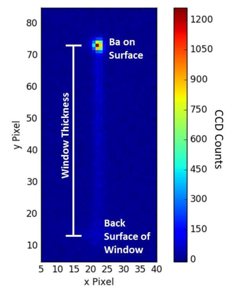
Extended Data Fig. 1: Example CCD image of a Ba+ deposit in SXe. The barium atoms are excited by a focused 570 nm laser, using a 620 nm fluorescence band-pass filter. The bright spot at the top of the image is the front surface of the window where the Ba ions are deposited. The broad spot at the bottom of the image is the surface fluorescence of back surface of the window. This spot is broadened due to the laser focus as well as the collection optics being optimized for the front surface. The faint line between the surfaces is the faint fluorescence of Cr3+ impurities in the bulk of the sapphire that extend into the filter region.
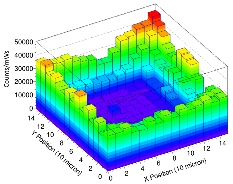
Extended Data Figure 2: Scan image of background emission after bleaching. A 532 nm laser was used to bleach the sapphire surface background in a 1414 grid pattern with 8 m steps. A 30 reduction of the background is observed in the low area where the bleaching laser was scanned.
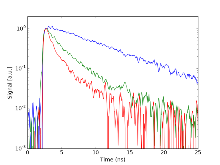
Extended Data Fig. 3: Time resolved photon counting of 619 nm fluorescence. Histograms of the 619 nm fluorescence decay of Ba in SXe (blue), SXe-only (green), and cryoprobe tube (red). The decay lifetime of the Ba fluorescence is 7.0 0.3 ns. The SXe-only and cryoprobe having shorter lifetimes of approximately 3 ns and 1.5 ns respectively.