Kirchhoff’s metasurfaces
Abstract
Thermo-optical properties of the nanodisc and metal hole array plasmonic perfect absorber (PPA) metasurfaces were designed and characterised at mid-infrared wavelengths. Both, light emitter and detector systems are highly thought after for the future sensor networks in the internet-of-things for various spectral domains. Reciprocity of the absorbance and emittance is shown experimentally, i.e., the PPAs are following Kirchhoff’s law where the patterns exhibiting a strong optical absorption were found enhanced thermal radiation. Design principles and scaling for photo-thermal conversion are discussed. The highest efficiency of light-to-heat and heat-to-radiation were obtained for the Au-Si-Au structures.
keywords:
mid infrared plasmonics, thermal radiation, photo-thermal generationControl of thermal radiation is one of challenges in the future’s essential technologies, which could deliver light emitters with tailored spectral, polarization, directionality properties strongly required for the infrared (IR) spectral window. According to the Einstein’s description of emission, the coefficient, , for the probability of spontaneous optical emission is smaller (a lower optical transition probability) at the mid-IR wavelength region as compared with the visible spectral range. Therefore, it would be expected that a mid-IR photo diode would have a low quantum efficiency of radiation/emission. For mid-IR wavelengths, the molecular vibrations have the representative absorbance bands and are used for qualitative and quantitative detection of different compounds, hence, realizing a molecular finger printing. Especially the mid-IR technology has focused on the gas sensing, exhaust control in cars, environmental monitoring, and human health care. The cavity ring down spectroscopy where a high finesse resonator is coupled with quantum cascade laser (QCLs) or a laser comb is one of the successful and promising technologies for optically detection of low concentration molecular species [1, 2, 3, 4, 5]. However, the cost of equipment such as QCL and comb lasers, highly reflectivity mirrors () at specific wavelengths, high speed photodiode detectors are still making this technology expensive and less portable.
Nowadays, the miniaturisation trend and information technology requires sensors for realizing the Internet-of-things (IoT) to become the founding principle of the future technologies [6, 7, 8, 9, 10]. The demand of IoT projects the following directions for sensors: low cost, portable (wearable), long lifetime (low energy consumption), and large quantities of sensors interconnected in the network [11, 12, 13]. Plasmonics and nanophotonics are the powerful candidates to contribute and solve the above mentioned challenges for IoT, especially for the chemical sensing field. An enhancement of the IR absorption by plasmons on nano-textured/pattered surfaces utilized in the surface-enhanced IR absorption (SEIRA) spectroscopy realize the high sensitivity and scaling along with the cost-down trend for entire sensing systems [14, 15, 16, 17, 18]. When the light emitters and detectors consist of the plasmonic materials, the strong EM-field enhancement factors would be expected for the enhanced emission efficiency as well as for the light absorption (the Kirchhoff’s law). A practical design of plasmon perfect absorbers (PPAs) has a configuration of a metal film, insulator (SiO2, Si, TiO2 or other dielectric), and metal nanostructure. Optical properties of the PPAs are zero transmission, , and close to zero reflection, , at the plasmon resonance. At the wavelength of plasmonic resonance, light should be absorbed by PPA [19, 20, 21, 22, 23, 24, 25, 26, 27, 28, 29]. For the ideal case, 100% of incident light can be absorbed at the resonance wavelength by PPA.
Kirchhoff’s law of radiation stipulates that the strong light absorber is also an efficient light emitter. Therefore PPA structures are expected to be also applicable for the light emitters, i.e., thermo-optical input/output devices. When plasmon materials absorbs at a specific wavelength, a decaying oscillation according to the quality Q-factor of the plasmonic resonance - oscillation of free electrons - generates Joule heat which is radiated. Experimental verification of Kirchhoff’s law at mid-far-IR wavelengths and for different absorption mechanisms in nanophotonic patterns and structures is strongly required.
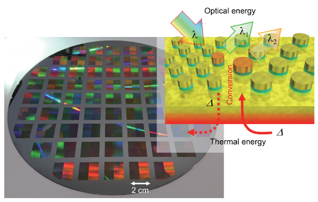
Here, we show a design of PPAs at IR wavelengths and tested them as optical emitters at IR wavelength. We experimentally characterise thermo-optical input and output properties of PPAs and show the reciprocity correlation between the absorbance and emittance of these Kirchhoff’s metasurfaces as shown in Fig.1.
1 Experimental
Fabrication of large area PPAs
Two type metasurfaces PPAs, the nano-disk and multi-hole array (NDA and MHA) nanostructures were fabricated on a silicon wafer via reduction projection photolithography using an -line stepper (NSR205-i14E, NIKON Co.) [30, 31]. First, a 200-nm-thick Au film has sputtered on the top of a double side polished Si wafer. The same photo mask pattern was used for both NDA and MHA fabrication. For NDAs a positive-tone photo-resist (TLOR-P003 HP, Tokyo Ohka Kogyo Co.), whereas for the MHA structures the negative tone resist (TLOR-N001 PM, Tokyo Ohka Kogyo Co.) was used. The resist pattern was developed for the following deposition of the insulator and metal structures deposited by magnetron sputtering with a sequence of 10 nm of Si/SiO2 and 50 nm of Au with a 3 nm Ti adhesion layer between Au and insulator (AXXIS, JKLesker). Then, the lift-off process followed in acetone for NDAs or methyl isobutyl ketone heated on a hot plate for MHAs. Both structures were rinsed by isopropanol and dried under nitrogen stream.
Optical characterization of PPAs
The optical reflection spectra were measured by conventional technique that is a combination of the FT-IR (FT-IR 4200, JASCO Co.) with a microscope unit (IRT-1000). As reference reflectivity, the Au mirror with 98% absolute reflectance was used. For the thermal radiation spectroscopy, the 8× times magnification Cassegrain reflector lens with numerical aperture was used. By controlling a square aperture, the 500 500 m2 region was measured.
Thermal radiation and photo-thermal conversion
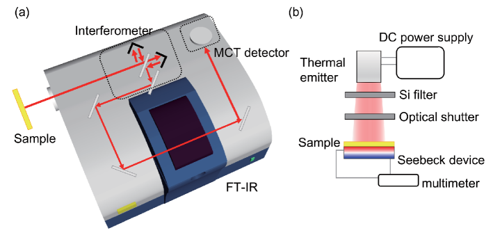
The thermal radiation and photo-thermal generation were measured by a custom home built setup. For realisation of FT-IR spectroscopy setup, the emitted light was passed through an interferometer. We have customized the commercial FT-IR (FT-IR 4200, JASCO Co.) as shown in Fig. 2(a). Light was coupled from outside into the FT-IR setup via an optical side-port. It passed through the interferometer and was detected on the HgCdTe (MCT) detector. Sample chamber was evacuated by oil rotary pump to reduce the absorption effect by CO2, H2O and other atmospheric gases in the present inside the measurement chamber. The target substrate was contacted to the ceramic heaters on the Al plate. The sample was heated at 300∘C; the temperature was monitored using radiative infrared thermometer.
Materials radiate the black body radiation according to their temperature with part of emission at the IR wavelengths. Most of the metals, which have high reflectivity have small emissivity. Therefore, an Al plate was used to block the IR thermal radiation that was generated from surrounding objects heated to 300∘C by the heater. Ceramic heater was also covered by Al to screen thermal radiation. To reduce the thermal noise form other sources, a top cover plate made by Al with 11 cm2 square through-hole was used and all the system was covered with Al film. This was required to measure the radiation from the sample. The radiation efficiency was determined using a relative radiation intensity of 94% of the black body using black ink (THL-1B TASCO Co.).
Photo-thermal conversion was measured using the Seebeck device as shown in Fig. 2-(b). Tungsten filament-based thermal radiation emitter was used for the IR-light source. A pseudo-collimated light was illuminated onto samples through a Si wafer, which works as a cut-filter under the 11its 00 n upgth light. The Si filter was separated enough from the heater to prevent its heat up by the tungsten heater. Sample was put on the Seebeck device on the Al plate. For the photo-thermal conversion, the sensitivity of Seebeck device was low, therefore a larger 22 cm2 region has illuminated, which contains four regions which were adjacent to each other. The output voltage from the Seebeck device has measured with a multimeter.
2 Results and discussion
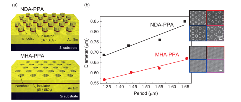
Figure 3(a) shows a schematic illustration of both, the nano-disk array (NDA) and multi-hole array (MHA) structures used for PPAs. Here, both metals in the PPA were gold because of the chemical stability for high temperature cycling in air conditions. As the insulator layer, Si and SiO2 were used to test influence of strongly different refractive index materials. The PPA patterns were fabricated uniformly over the 11 cm2 area. Different hole (disk) diameters and periods of the pattern were tested. The periods and diameters of the NDA and MHA structures is plotted in the Fig. 3(b). The same mask was used for both, the NDA and MHA structures and the period was reliably reproduced. However, the diameters of the disks and holes were slightly different. The ratio of the diameter-to-period was set to the 1:2. The NDA structures were reproduced according to the design, while the MHA patterns showed slightly smaller holes. This is due to different retention of the polymer vs. dose for the used negative and positive tone resists.
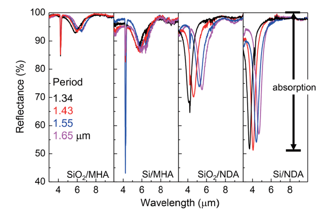
Figure 4 shows the optical reflection spectra for the NDA and MHA structures. The PPAs had a 200-nm-thick Au film on the bottom of the structure. Therefore no transmission of light can be observed in experiment (transmission data has been omitted in Fig.4) and light (except scattering and reflection) is absorbed in the PPA structure. The sharp peaks around 4.3 m are caused by CO2 absorption in air, which could be removed by N2 purging when required.
Noteworthy, when we consider typical plasmonic resonances, the NDAs were inspected in the reflection or scattering while the MHAs were measured in the transmission mode for comparison of their performance as absorbers. The MHA showed considerably smaller reflection dip, which means a weaker absorption at the plasmonic resonance. However, the NDAs showed a strong absorption, hence, modulation of the reflectance at the resonance wavelength. For both structures, the Si insulator was preferable due to the larger absorption as compared with SiO2 (Fig. 4).
The plasmon peak wavelength is dependent on the geometry of the structure. In NDAs, it is mainly defined by the diameter of the disc, while in MHA by the period. Considering typical MHA structures, their performance as absorbers had a weaker dependence on the structure period (Fig. 4).
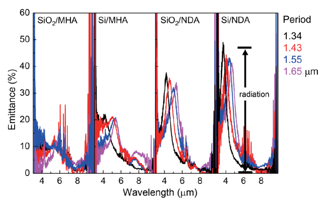
Figure 5 summaries thermal radiation properties of the very same PPAs characterized above for their absorbance. To obtain emittance, the radiation spectra was normalized to the sample that was covered with a 94% radiation efficiency black body ink. As expected from the Kirchhoff’s law, the spectral shape of emittance was strongly anti-correlated with the reflectivity spectrum of the same structure (or the absorbance is correlated with emittance). The peak emittance agreed well with the spectral position of absorption maximum (a dip in reflectance). According to the Kirchhoff’s law of the thermal radiation, the thermal emission and absorption are expected to be equal under the thermodynamic equilibrium condition.
The NDA absorber structure with Si insulator presents the most effective emitter among the tested four. With the PPA it would be possible to realize the perfect absorption: a zero-transmission and reflection, hence, a 100% absorption, when the impedance matching to the air has been achieved [32]. For this purpose, the dielectric permittivity of the structures, substrate and insulator layer and their thickness optimization is required.
Thermo-emitter response of the PPAs is shown in Fig. 6 where Seebeck voltage is presented (see, Fig. 2(b)). A time dependent response to the on-off switching of the IR light is presented in (a); switching was controlled by a mechanical shutter within 0.7 s time intervals. Both ”on” and ”off” response times to the saturated state of the Seebeck voltage took few tens of seconds for all samples. This is caused by the time required to diffuse heat through an entire thickness of the substrate. In Fig. 6(b), the maximum output voltage is shown. All the PPA structures exhibited a larger efficiency of thermal emission as compared to the 0.5-mm-thick Al plate and 200-nm-thick Au films on Si (which is the same substrate without top nanostructures). Metals such as Al and Au have a lower absorption coefficient and consequently have a lower emissivity: Al 4-8% and Au 2-3%, respectively [33]. Even in the mid-IR range, there is a weak interband absorption in metals (hence emission). Both metal surface have some roughness that can facilitate coupling of the incident light into a surface plasmon polariton wave. Therefore, there were still some photo-thermal heat generation present using these substrates. It is important to separate the effect which is not caused by the designed structure, especially for the Au-Si substrate with the same composition as PPAs. The output form the Au-Si served as a reference for the background of the plasmonic absorber/emitter (Fig. 6(b)).
Experiments clearly show that the thermal emission from PPAs was stronger than background noise from unstructured samples made from the same materials. The Seebeck device (Fig 2(b)) used in this study was linear at around room temperature [34]. Thermal emission from PPAs was estimated to be at least from 2.5 to 3.0 times stronger than that from the Al plate.

The tungsten thermal emitter (Fig. 2(b)) covers a wide wavelength range where it performs close to the blackbody radiation efficiency. In this experiment, samples with four different periods were illuminated. The plasmon band of the PPAs are narrow in the tested wavelength range and the differences in geometry between samples were rather small. The averaged PPA absorbance was from 2.7 to 7.8% in this wavelength region. Therefore the output thermal emission was expected to be small. Illumination of PPAs by monochromatic light from mid-IR laser, light emitting diode can be used to characterise PPA detectors and is considered for a future study.
The temperature change was estimated to be from 0.01 K (Al plate) to 0.03 K (Si-NDA). A large heat conductivity and thick substrate would dissipate heat to air and it decrease contrast from the thermal background. The response time to reach saturation (equilibration) is dependent of the thermal capacitance. Integration of PPAs on thermally isolated membrane could help to reduce the thermal background noise and to increase the temperature of the PPA. It could help to realize a plasmon micro-bolometer working at room temperature.
FDTD calculations
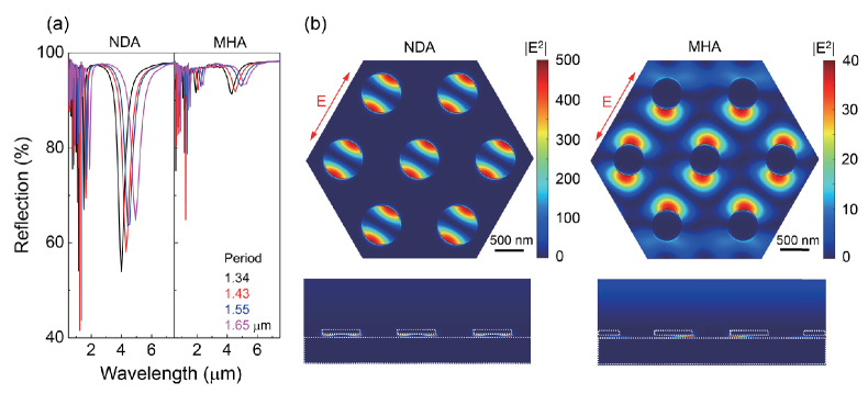
The FDTD calculations were performed for the ideal shape of the flat surface of the metal and insulator. Figure 7(a) shows the optical reflection spectra of PPAs as used in experiments. Absorbance of NDA was more than 4 times larger than that of MHA. From the electromagnetic field profile at the resonance wavelength shown in Fig. 7(b) it follows that the E-field is localized in the insulator layer. As described in the experimental section, the insulator layer was at the bottom of metal structures. However in the case of MHA-PPAs, the insulator layer was continuous overall the entire sample, E-field is delocalized and absorption was smaller than that of NDA structures.
The basic scaling behaviour of PPAs observed in experiments and differences between MHA and NDA patterns can be gauged from this simple FDTD model to reveal the localization of energy and local field enhancement. In the case of SiO2 insulator layer, the modeled optical properties were closely following the experimental results.
As our previous work indicated, the surface roughness of the structures, especially the metal base, affects numerical results considerably. Therefore it is important to reproduce a closely matching resemblance of the experimental PPA when it is rendered for FDTD modeling seeking more quantitative match with experiments. It was found that FDTD predictions of PPAs with Si insulator layer show differences with experimental observations due to electrical conductivity of Si (which is accounted for via permittivity of materials used in numerical simulations) [31].
Conclusions and Outlook
It is demonstrated that NDA and MHA structures made for resonant absorbance are performing as the narrow band thermal radiation emitters. The energy conversion for thermal energy harvesting as well as extraction into radiation are feasible. The most efficient thermal emitters had the NDA design with Si as insulator for the IR wavelengths.
Kirchhoff’s metasurfaces can find applications for thermal emitters and detectors and open a toolbox for engineering thermal energy control for miniaturised (wavelength scale) devices in IR spectral range. Since Si has comparatively high transparency in THz spectral range, we can envisage application of such Kirchhoff’s metasurfaces over a broad spectral range. Next modality in IR emission control is creation of directional IR emitters by harnessing the Wolf’s effect [35] with a grating over the Kirchhoff’s metasurfaces. Such surface will deliver angular selectivity and enhancement of light extracted with the sub-wavelength grating realizing a coherent IR emitter [35, 36].
acknowledgement
Authors are grateful for the Tokyo Ohka Kogyo Co. Ltd. for access to stepper. YN and SN gratefully thank Dr. Hideki Miyazaki from National institute for material science for advise regarding construction of thermal radiation measurement setup. YN is grateful for partial support by Japan Society for the Promotion of Science (JSPS), Grants-in-Aid for Scientific Research, Open Partnership Joint Projects of JSPS Bilateral Joint Research Projects, Tateishi and Amada fundations. SJ acknowledges partial support via the Australian Research Council Discovery project DP130101205 and a startup funding of Nanotechnology facility by Swinburne University.
References
- Wheeler et al. [1998] M. D. Wheeler, S. M. Newman, A. J. Orr-Ewing, M. N. R. Ashfold, Cavity ring-down spectroscopy, J. Chem. Soc., Faraday Trans 94 (1998) 337–351.
- Zalicki and Zare [1995] P. Zalicki, R. N. Zare, Cavity ring-down spectroscopy for quantitative absorption measurements, J. Chem. Phys. 102 (1995) 2708.
- Berden et al. [2000] G. Berden, R. Peeters, G. Meijer, Cavity ring-down spectroscopy: Experimental schemes and applications, Int. Rev. Phys. Chem. 19 (2000) 565–607.
- Sun et al. [2018] J. Sun, J. Ding, N. Liu, G. Yang, J. Li, Detection of multiple chemicals based on external cavity quantum cascade laser spectroscopy, Spectroc. Acta Pt. A-Molec. Biomolec. Spectr. 191 (2018) 532–538.
- Kiseleva et al. [2018] M. Kiseleva, J. Mandon, S. Persijn, F. Harren, Line strength measurements and relative isotopic ratio 13c/12c measurements in carbon dioxide using cavity ring down spectroscopy, J. Quant. Spectrosc. Radiat. Transf. 204 (2018) 152–158.
- Bandodkar et al. [2016] A. J. Bandodkar, I. Jeerapan, J. Wang, Wearable chemical sensors: present challenges and future prospects, ACS Sens. 1 (2016) 464–482.
- Khan et al. [2015] S. Khan, L. Lorenzelli, R. S. Dahiya, Technologies for printing sensors and electronics over large flexible substrates: A review, IEEE Sens. J. 15 (2015) 3164–3185.
- Caldara et al. [2016] M. Caldara, C. Colleoni, E. Guido, V. Re, G. Rosace, Optical monitoring of sweat ph by a textile fabric wearable sensor based on covalently bonded litmus-3-glycidoxypropyltrimethoxysilane coating, Sens. Actuators, B 222 (2016) 213–220.
- Senior [2014] M. Senior, Novartis signs up for google smart lens, Nat. Biotechnol 32 (2014) 856.
- Mannoor et al. [2012] M. S. Mannoor, H. Tao, J. D. Clayton, A. Sengupta, D. L. Kaplan, R. R. Naik, N. Verma, F. G. Omenetto, M. C. McAlpine, Graphene-based wireless bacteria detection on tooth enamel, Nat. Commun 3 (2012) 763.
- Güntner et al. [2016] A. T. Güntner, V. Koren, K. Chikkadi, M. Righettoni, S. E. Pratsinis, E-nose sensing of low-ppb formaldehyde in gas mixtures at high relative humidity for breath screening of lung cancer, ACS Sens. 1 (2016) 528–535.
- Maruyama et al. [2018] S. Maruyama, T. Hizawa, K. Takahashi, K. Sawada, Optical-interferometry-based cmos-mems sensor transduced by stress-induced nanomechanical deflection, Sensors 18 (2018) 138.
- Adib et al. [2018] M. Adib, R. Eckstein, G. Hernandez-Sosa, M. Sommer, U. Lemmer, Sno2 nanowire-based aerosol jet printed electronic nose as fire detector, IEEE Sens. J. 18 (2018) 494–500.
- Nishijima et al. [2012] Y. Nishijima, H. Nigorinuma, L. Rosa, S. Juodkazis, Selective enhancement of infrared absorption with metal hole allays, Opt. Mater. Express 2 (2012) 1367.
- Nishijima et al. [2013] Y. Nishijima, Y. Adachi, L. Rosa, S. Juodkazis, Augmented sensitivity of an ir-absorption gas sensor employing a metal hole array, Opt. Mat. Express 32 (2013) 968.
- Nishijima et al. [2017] Y. Nishijima, S. Suda, G. Seniutinas, A. Balčytis, S. Juodkazis, Plasmonic sensor: towards parts-per-billion level sensitivity, Sens. Mater. 29 (2017) 1253–1258.
- Brown et al. [2015] L. V. Brown, X. Yang, Z. K, B. Y. Zheng, P. Nordlander, N. J. Halas, Fan-shaped gold nanoantennas above reflective substrates for surface-enhanced infrared absorption (seira), Nano Lett. 15 (2015) 1272–1280.
- Dong et al. [2017] L. Dong, X. Yang, C. Zhang, B. Cerjan, L. Zhou, M. L. Tseng, Y. Zhang, A. Alabastri, P. Nordlander, N. J. Halas, Nanogapped au antennas for ultrasensitive surface-enhanced infrared absorption spectroscopy, Nano Lett. 17 (2017) 5768–5774.
- Diem et al. [2009] M. Diem, T. Koschny, C. M. Soukoulis, Wide-angle perfect absorber/thermal emitter in the thz regime, Phys. Rev. B 79 (2009) 033103.
- Miyazaki et al. [2014] H. Miyazaki, T. Kasaya, M. Iwanaga, C. Bongseok, Y. Sugimoto, K. Sakoda, Dual-band infrared metasurface thermal emitter for co2 sensing, Appl. Phys. Lett. 105 (2014) 121107.
- Miyazaki et al. [2008] H. T. Miyazaki, K. Ikeda, T. Kasaya, K. Yamamoto, Y. Inoue, K. Fujimura, T. Kanakugi, M. Okada, K. Hatade, S. Kitagawa, Thermal emission of two-color polarized infrared waves from integrated plasmon cavities, Appl. Phys. Lett. 92 (2008) 141114.
- Ikeda et al. [2008] K. Ikeda, H. T. Miyazak, T. Kasaya, K. Yamamoto, Y. Inoue, K. Fujimura, T. Kanakugi, M. Okada, K. Hatade, S. Kitagawa, Controlled thermal emission of polarized infrared waves from arrayed plasmon nanocavities, Appl. Phys. Lett. 92 (2008) 021117.
- Kusunoki et al. [2004] F. Kusunoki, T. Kohama, T. Hiroshima, S. Fukumoto, J. Takahara, T. Kobayashi, Narrow-band thermal radiation with low rirectivity by resonant modes inside tungsten microcavities, Jpn. J. Appl. Phys. 43 (2004) 5253.
- Ueba and Takahara [2012] Y. Ueba, J. Takahara, Spectral control of thermal radiation by metasurface with split-ring resonator, Appl. Phys. Express 5 (2012) 122001.
- Maruyama et al. [2001] S. Maruyama, T. Kashiwa, H. Yugami, M. Esashi, Thermal radiation from two-dimensionally confined modes in microcavities, Appl. Phys. Lett. 79 (2001) 1393.
- Liu et al. [2010] N. Liu, M. Mesch, T. Weiss, M. Hentschel, H. Giessen, Infrared perfect absorber and its application as plasmonic sensor, Nano Lett. 10 (2010) 2342–2348.
- Hedayati et al. [2014] M. K. Hedayati, F. Faupel, M. Elbahri, Review of plasmonic nanocomposite metamaterial absorber, Materials 7 (2014) 1221–1248.
- DESHPANDE et al. [2017] R. DESHPANDE, A. PORS, S. I. Bozhevolnyi, Third-order gap plasmon based metasurfaces for visible light, Opt. Express 25 (2017) 12508–12517.
- Leveque and Martin [2006] G. Leveque, O. J. F. Martin, Optical interactions in a plasmonic particle coupled to a metallic film, Opt. Express 14 (2006) 9971–9981.
- Nishijima et al. [2017] Y. Nishijima, A. Balčytis, G. Seniutinas, S. Juodkazis, T. Arakawa, S. Okazaki, R. Petruskevicius, Plasmonic hydrogen sensor at infrared wavelength, Sens. Mater. 29 (2017) 1269–1274.
- Nishijima et al. [????] Y. Nishijima, A. Balčytis, S. Naganuma, G. Seniutinas, S. Juodkazis, Tailoring metal and insulator contributions in plasmonic perfect absorber metasurfaces, submitted to ChemRxiv (????).
- Pu et al. [2011] M. Pu, C. Hu, M. Wang, C. Huang, Z. Zhao, C. Wang, Q. Feng, X. Luo, Design principles for infrared wide-angle perfect absorber based on plasmonic structure, Opt. Express 19 (2011) 17413–17420.
- Brewster [1992] M. Q. Brewster, Thermal radiative transfer and properties (1992).
- Komatsua et al. [2015] R. Komatsua, A. Balčytis, G. Seniutinas, T. Yamamura, Y. Nishijima, S. Juodkazis, Plasmonic photo-thermoelectric energy converter with black-si absorber, Sol. Ener. Mater. Sol. Cell 143 (2015) 72–77.
- Greffet et al. [2002] J.-J. Greffet, R. Carminati, K. Joulain, J.-P. Mulet, S. Mainguy, Y. Chen, Coherent emission of light by thermal sources, Nature 416 (2002) 61–64.
- Liu et al. [2015] J. Liu, U. Guler, A. Lagutchev, A. Kildishev, O. Malis, A. Boltasseva, V. M. Shalaev, Quasi-coherent thermal emitter based on refractory plasmonic materials, Opt. Mater. Express 5 (2015) 2721–2728.