Superconducting cavity electro-optics: a platform for coherent photon conversion between superconducting and photonic circuits
Leveraging the quantum information processing ability of superconducting circuits and long-distance distribution ability of optical photons promises the realization of complex and large-scale quantum networks. In such a scheme, a coherent and efficient quantum transducer between superconducting and photonic circuits is critical. However, such quantum transducer is still challenging since the use of intermediate excitations in current schemes introduces extra noise and limits bandwidth. Here we realize direct and coherent transduction between superconducting and photonic circuits based on triple-resonance electro-optics principle, with integrated devices incorporating both superconducting and optical cavities on the same chip. Electromagnetically induced transparency is observed, indicating the coherent interaction between microwave and optical photons. Internal conversion efficiency of has been achieved, with total efficiency. Superconducting cavity electro-optics offers broad transduction bandwidth and high scalability, and represents a significant step towards the integrated hybrid quantum circuits and distributed quantum computation.
Introduction
The hybrid approach of combining superconducting and photonic quantum technologies promises to realize large scale quantum networks (Schoelkopf and Girvin, 2008; O’brien et al., 2009; Lvovsky et al., 2009; Xiang et al., 2013). In superconducting quantum circuits, the low-loss single quanta nonlinearity at microwave frequencies inherent to Josephson effect allows efficient and fast quantum operations (Clarke and Wilhelm, 2008). However, it is challenging to directly transmit quantum states at microwave frequencies over long distance due to the high attenuation and thermal noise at room temperature. On the other hand, optical photons show complementary features. The weak single photon nonlinearity prevents the development of high fidelity quantum gates at optical frequency (Kok et al., 2007). However, low decoherence and dissipation rates make optical photons the ideal information carrier for quantum communication (O’brien et al., 2009; Lvovsky et al., 2009). As a result, it is beneficial to develop hybrid quantum platform where quantum information is processed by superconducting circuits, and transmitted with optical photons. Thus, the quantum transducer which can coherently interface superconducting and photonic circuits with high conversion efficiency is highly demanded (Andrews et al., 2014; Bochmann et al., 2013; Balram et al., 2016; Barzanjeh et al., 2012; Lecocq et al., 2016; Tsang, 2010, 2011; Huang, 2015; Javerzac-Galy et al., 2016; Rueda et al., 2016; Soltani et al., 2017; Hafezi et al., 2012; Hisatomi et al., 2016; Williamson et al., 2014).
Coherent conversion of photons between microwave and optical frequencies has been proposed utilizing various intermediate excitations, including collective spin in atom ensembles (Hafezi et al., 2012), phonon in electro-optomechanics (Barzanjeh et al., 2012; Bochmann et al., 2013; Andrews et al., 2014; Balram et al., 2016), and magnon in magneto-optics (Hisatomi et al., 2016; Williamson et al., 2014). Currently, the highest conversion efficiency is demonstrated based on electro-optomechanical systems where a compliant mechanical resonator couples to microwave and optical cavities simultaneously (Andrews et al., 2014). The use of intermediate low-frequency (MHz) excitations inevitably introduces extra noise channels, limits conversion bandwidth, and complicates operation with impedance matching between optical and microwave ports. The electro-optic approach can overcome these obstacles by excluding intermediate excitations in the conversion process, as proposed by Tsang recently (Tsang, 2010, 2011). Great improvement of electro-optic coupling strength is proposed by Javerzac-Galy et al. utilizing coplanar microwave structure and integrated optical resonators, showing the feasibility of near-unity conversion efficiency with practical device parameters (Javerzac-Galy et al., 2016). Even though the conversion efficiency of electro-optical systems has been improved dramatically, it is still limited to ~0.1% due to the large ohmic loss of non-superconducting material, and small coupling rates resulting from large mode volumes (Rueda et al., 2016). Moreover, the coherence and bidirectionality of the conversion process remain to be proved.
In this paper, we report the experimental demonstration of the coherent conversion between microwave and optical photons based on the electro-optic effect within a hybrid superconducting-photonic device, where planar superconducting resonators are integrated with aluminum nitride (AlN) optical cavities on the same chip. We observe the electromagnetically induced transparency effect in electo-optic systems, as a signature of coherent conversion between microwave and optical photons. Internal conversion efficiency of and on-chip efficiency of are realized. A major challenge we have addressed is to realize the energy and phase conservation of the triple-resonance condition with ultra-small mode volumes, boosting the pump photon number and vacuum coupling rate simultaneously to enhance the coherent conversion. Moreover, our device is ready to incorporate other superconducting and photonic quantum devices on the same chip, providing the scalable platform for hybrid quantum network.
Results
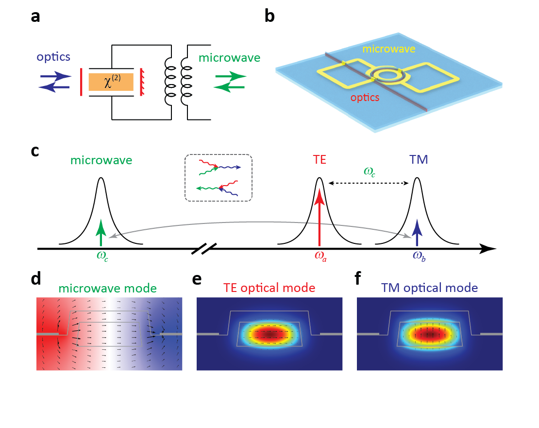
The principle of quantum transducers based on superconducting cavity electro-optics is illustrated in Fig. 1A. The optical cavity, consisting of materials with Pockel nonlinearity, is placed inside the capacitor of the LC microwave resonator. The electric field across the capacitor changes the refractive index of the optical cavity, thus modulates the optical resonant frequency. Reversely, modulated optical fields can generate microwave field due to the optical mixing (rectification) in Pockels materials (Bass et al., 1962). To implement the quantum transducer, we use integrated optical microring cavities made of AlN, which supports low loss optical modes and provides high electro-optic coefficients simultaneously (Xiong et al., 2012) (Fig. 1B). Superconducting microwave resonators are placed on top of a thin buffer layer, and the capacitor shape is designed to match the optical cavity to maximize the field overlap between microwave and optical modes (Javerzac-Galy et al., 2016; Soltani et al., 2017).
We employ the triple-resonance scheme to enhance the coupling as shown Fig. 1C, with the interaction Hamiltonian written as
where , , are the annihilation operators for the optical pump and signal modes, and microwave mode respectively, and is the vacuum electro-optic coupling rate. Cavity electro-optic systems with triple resonances have been proposed and demonstrated recently (Javerzac-Galy et al., 2016; Rueda et al., 2016). However, the device geometry is limited to above several millimeters, as the pump and signal optical modes are from the same mode group, and the free spectral range (FSR) needs to match the microwave frequency. Large mode volume inevitably leads to small vacuum coupling rate, thus low conversion efficiency (Supplementary Section I). In contrast, our integrated approach uses the transverse-electric (TE) and transverse-magnetic (TM) optical modes as pump and signal modes respectively (Fig. 1E & F), whose frequency difference equals the microwave frequency (Ilchenko et al., 2002, 2003; Savchenkov et al., 2009; Strekalov et al., 2009). Thus the device size and mode volume can be further reduced without the limitation imposed by FSR. In this case, electro-optic coefficient is used, which also enables the use of TE-polarized microwave mode, thus the heterogeneous integration of planar microwave resonators with optical cavities (Fig. 1D). During experiments, a strong coherent field is applied to the pump mode () to stimulate the coherent coupling between signal mode () and microwave mode (), and photons can be bidirectionally converted between optical and microwave frequencies with on-chip efficiency
| (1) |
where , , , are the external coupling and total loss rates for signal and microwave modes respectively, and is the cooperativity with the photon number in the pump mode (Supplementary Section I).
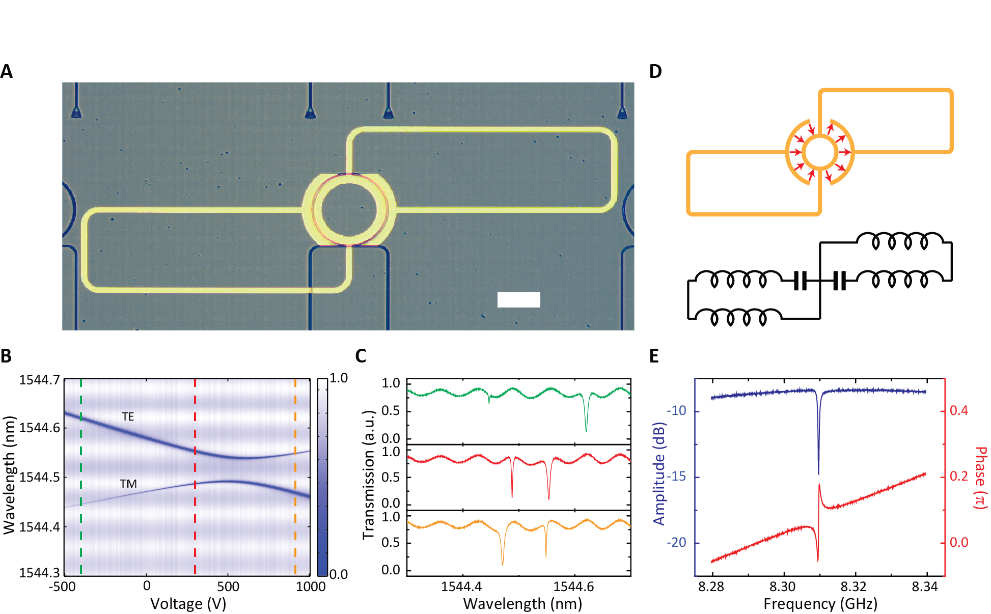
In experiments, the optical cavity is fabricated from an AlN layer on a silicon dioxide cladding on silicon wafer (Fig. 2A). The optical ring cavity has a radius of , and cross-section of (See Supplementary Section II for fabrication procedure and device cross-section). An azimuthal number difference of 1 between the pump and signal optical modes is chosen to mitigate the optical mode mixing induced by the non-vertical waveguide sidewalls (See Supplementary Section III for the identification of azimuthal number difference, and Supplementary Section IV for the influence of TE/TM mode mixing). In Fig. 2B, we present the transmission of TE input light, where mode anti-crossing is observed arising from the structural asymmetry and fabrication imperfection. As TE and TM optical modes have opposite electro-optic coefficients, DC voltage is applied across the device to tune the frequency difference precisely in a wide spectrum range. Compared with using optical modes from the same group (Javerzac-Galy et al., 2016; Rueda et al., 2016), the large frequency tuning range of our device makes it easy to accommodate different microwave frequencies within a single device.
The microwave resonator is made of NbTiN superconducting film with critical temperature around . The device is placed in a cryostat and cooled down to 2 K, and the device surface is covered by superfluid helium to introduce fast heat dissipation (Sun et al., 2013). To allow electro-optic phase matching, it is important to shape the microwave resonator to have azimuthal number of 1, to match the azimuthal number difference between the pump and signal modes (Fig. 2D & Supplementary Section V). The capacitance part of the microwave resonator has a radius of to match the optical cavity, and the distance between electrodes is . Each inductance arm has a length of , allowing far-field magnetic coupling to an off-chip loop probe for broadband microwave signal input and readout. The microwave mode has resonance around with the decay rate of at (Fig. 2E). When the DC voltage is tuned to , the frequency difference between pump and signal modes is also around (Fig. 2C). Therefore, the phase matching and energy conservation are fulfilled simultaneously.
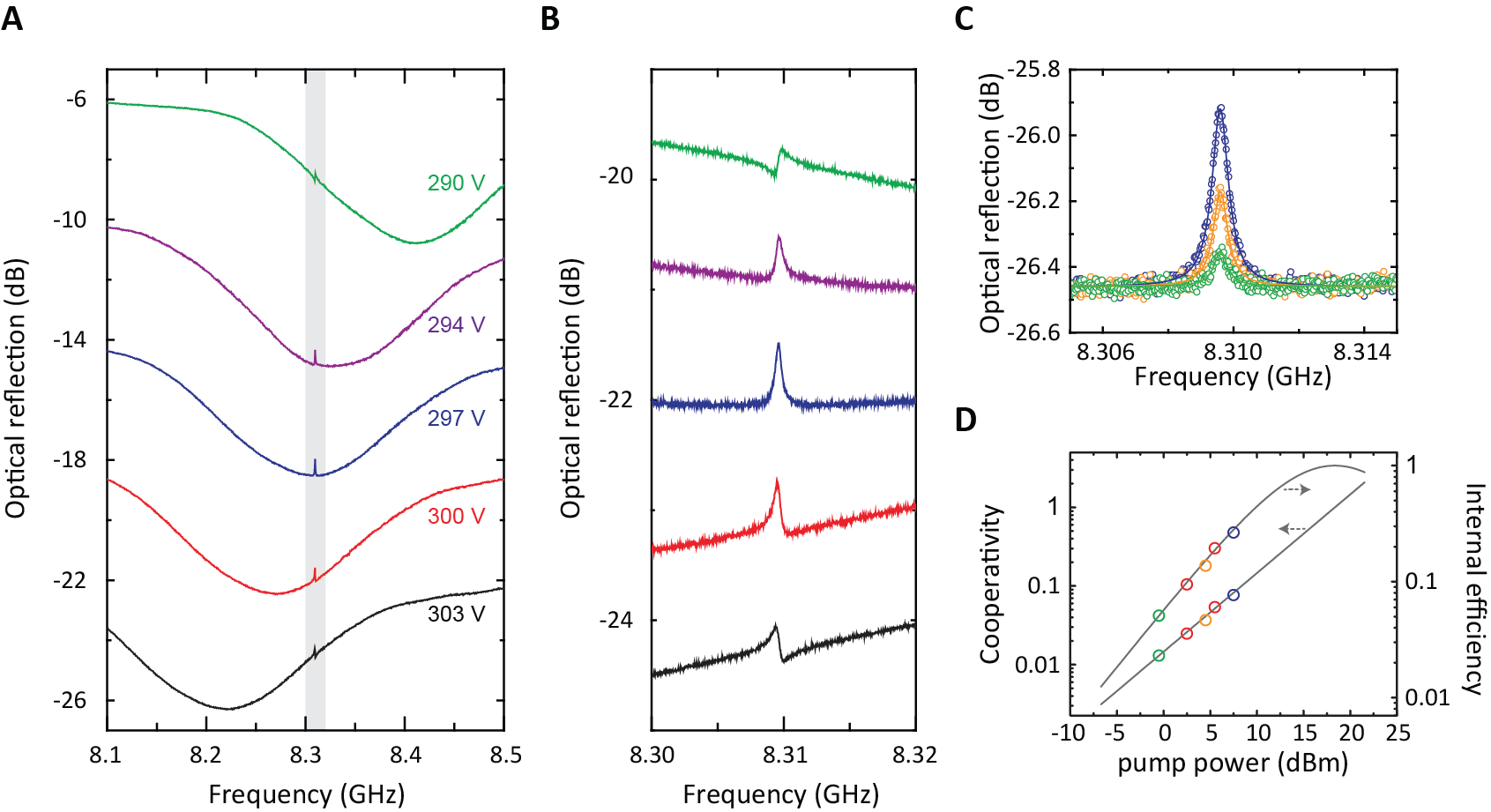
The coherent conversion of our device is first characterized with optical reflection spectrum. Strong control light is applied to the pump mode, and a weak probe light, derived from the control light by single side-band modulation, is sent to the signal mode (Supplementary Section VI). No obvious temperature change of the superconducting microwave resonator is observed (Supplementary Section VII). Figure 3A presents the probe light transmission spectrum sweeping across the signal mode, with a fixed control light on resonance with the pump mode. By tuning the DC voltage, the broad Lorentzian dip corresponding to the signal mode is shifted, with a sharp modification of the spectrum at a fixed frequency . This modification originates from the destructive interference between two pathways for the probe light: directly passing through the optical cavity, and converting to microwave photons and then back to optical photons (Weis et al., 2010; Safavi-Naeini et al., 2011). As shown in the enlarged spectrum (Fig. 3B), when the signal mode frequency matches , there is a sharp transparency window, with the bandwidth equal to . If the signal mode is detuned, the interference gives an asymmetric Fano-shape spectrum. By fitting the transparency window, the conversion cooperativity can be extracted, and internal conversion efficiency can be inferred (Fig. 3C & D) (Hill et al., 2012). An internal efficiency as high as is achieved with our device under 8 dBm control light power (14 dBm total off-chip optical power with 6 dB insertion loss).
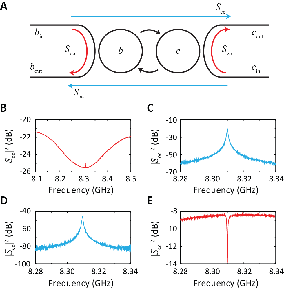
The bidirectional conversion is characterized by measuring the complete conversion matrix (Fig. 4A) with the DC voltage fixed at . By injecting the optical probe and monitoring the microwave output, we measure the microwave-to-optical coefficient , which is a Lorentzian lineshape centered at the microwave resonant frequency (Fig. 4C). The optical-to-microwave coefficient is measured by reversing the input and output signal, which has the same spectrum shape with microwave-to-optical coefficient , indicating that the conversion is bidirectional (Fig. 4D). The optical and microwave reflection spectra are also measured for calibration (Fig. 4B & E), and the on-chip efficiency is estimated to be (Supplementary Section VIII). The main noise source during the conversion process is the thermal excitation of the microwave cavity, which can be reduced by working at lower temperature. And the noise generated by the parametric amplification process is negligible because of the deep resolved sideband condition (Supplementary Section IX).
Discussion
An ideal quantum transducer demands the coherent conversion efficiency approaching , when the cooperativity equals unity and both microwave and optical modes are deeply over-coupled. By optimizing the fabrication process and material properties, the efficiency of our device can be further increased. For instance, optical quality factors above 2 million have been demonstrated with single crystalline AlN (Liu et al., 2017), therefore intrinsic loss for optical modes can be reduced to . Then, pump photon number can be increased by ~100 times with the same pump power, and the enhanced coupling rate can reach . With an improved microwave intrinsic loss rate of (Bruno et al., 2015), for example by using sapphire substrate, the optimal on-chip efficiency exceeding can be achieved by choosing the external optical coupling rate and microwave coupling rate . Therefore, with future development of single crystalline AlN on sapphire system and its adaption for superconducting resonators, the approach presented here is promising to realize high fidelity quantum state transduction between superconducting and photonic circuits.
Conclusion
We have demonstrated the coherent photon transduction between integrated superconducting and photonic circuits. High transduction efficiency is realized based on triple-resonance electro-optics principle. Besides high efficiency, low noise, and large bandwidth, the large frequency tunability makes it easy to interface with different quantum systems, and the planar structure allows the circuit-level integration of different quantum devices. All these features not only make our device an ideal quantum transducer, but also provide a scalable platform to synthesize different quantum systems, paving the route towards large scale hybrid quantum networks.
Materials and Methods
Polycrystal AlN film preparation The 800 nm AlN film is grown on a Si wafer with 2--thick layer by the radio frequency magnetron reactive sputtering, using pure aluminum (99.999%) targets in an argon and nitrogen gas mixture. The sputtered AlN film is poly-crystal with -axis highly oriented perpendicular to the substrate. As AlN has wurtzite crystal structure, the electro-optic coefficient has no direction dependence in the plain perpendicular to -axis. Thus the coefficient in the sputtered AlN film can be used without considering the in-plain crystal direction change (Xiong et al., 2012).
NbTiN film preparation NbTiN films are sputtered by the RF magnetron method at room temperature using 70% Nb and 30% Ti alloy target in an argon and nitrogen gas mixture. Amouphous NbTiN film is formed uniformly on the surface, and the superconducting critical temperature around is achieved.
Supplementary Materials
Theory of cavity electro-optics and its utility for microwave-to-optical conversion
Device fabrication procedure
Identifying phase matching conditions for optical modes
Influence of optical mode mixing on the vacuum coupling rate
Microwave resonator design
Measurement setup
Device temperature calibration
Efficiency calibration
Added noise during conversion
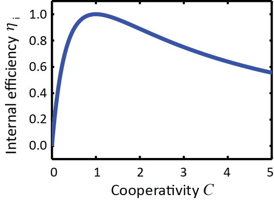
Fig. S1. Calculated internal conversion efficienty
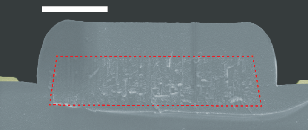
Fig. S1. SEM picture of the cross section of a superconducting cavity electro-optic device
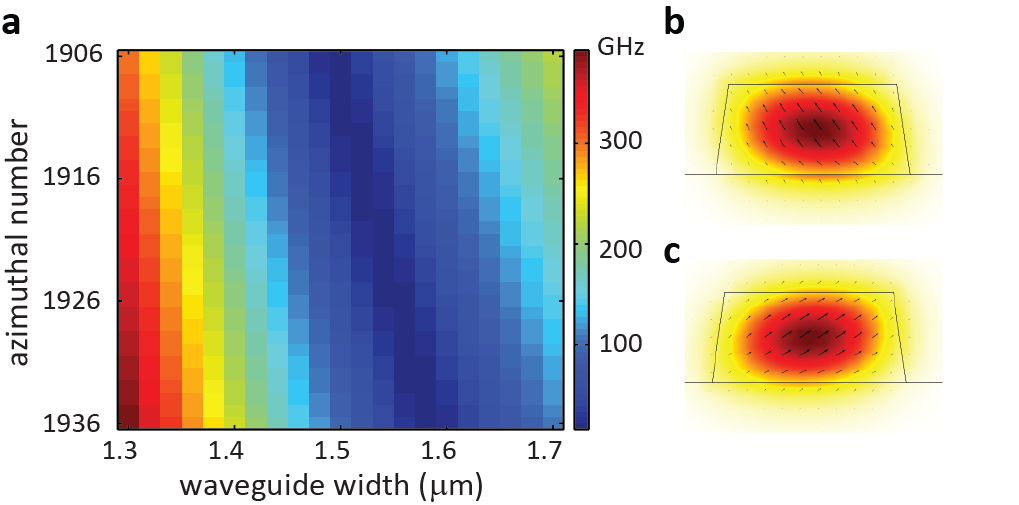
Fig. S3. Anti-crossing between TE and TM optical modes.
Fig. S4. Measured spectrum signature of mixing between TE and TM modes
Fig. S5. Wavelength dierence between adjacent resonances
Fig. S6. Phase matching wavelength and anti-crossing strength
Fig. S7. Vacuum coupling rate with hybrid optical modes
Fig. S8. Microwave resonator simulation
Fig. S9. Experiment setup for microwave-to-optical photon conversion
Fig. S10. Microwave resonator performance under different temperature
References and Notes
References
- Schoelkopf and Girvin (2008) R. Schoelkopf and S. Girvin, “Wiring up quantum systems,” Nature 451, 664 (2008).
- O’brien et al. (2009) J. L. O’brien, A. Furusawa, and J. Vučković, “Photonic quantum technologies,” Nature Photonics 3, 687 (2009).
- Lvovsky et al. (2009) A. I. Lvovsky, B. C. Sanders, and W. Tittel, “Optical quantum memory,” Nature photonics 3, 706 (2009).
- Xiang et al. (2013) Z.-L. Xiang, S. Ashhab, J. You, and F. Nori, “Hybrid quantum circuits: Superconducting circuits interacting with other quantum systems,” Reviews of Modern Physics 85, 623 (2013).
- Clarke and Wilhelm (2008) J. Clarke and F. K. Wilhelm, “Superconducting quantum bits,” Nature 453, 1031 (2008).
- Kok et al. (2007) P. Kok, W. J. Munro, K. Nemoto, T. C. Ralph, J. P. Dowling, and G. J. Milburn, “Linear optical quantum computing with photonic qubits,” Reviews of Modern Physics 79, 135 (2007).
- Andrews et al. (2014) R. W. Andrews, R. W. Peterson, T. P. Purdy, K. Cicak, R. W. Simmonds, C. A. Regal, and K. W. Lehnert, “Bidirectional and efficient conversion between microwave and optical light,” Nature Physics 10, 321 (2014).
- Bochmann et al. (2013) J. Bochmann, A. Vainsencher, D. D. Awschalom, and A. N. Cleland, “Nanomechanical coupling between microwave and optical photons,” Nature Physics 9, 712 (2013).
- Balram et al. (2016) K. C. Balram, M. I. Davanço, J. D. Song, and K. Srinivasan, “Coherent coupling between radiofrequency, optical and acoustic waves in piezo-optomechanical circuits,” Nature photonics 10, 346 (2016).
- Barzanjeh et al. (2012) S. Barzanjeh, M. Abdi, G. J. Milburn, P. Tombesi, and D. Vitali, “Reversible optical-to-microwave quantum interface,” Physical Review Letters 109, 130503 (2012).
- Lecocq et al. (2016) F. Lecocq, J. B. Clark, R. W. Simmonds, J. Aumentado, and J. D. Teufel, “Mechanically mediated microwave frequency conversion in the quantum regime,” Physical review letters 116, 043601 (2016).
- Tsang (2010) M. Tsang, “Cavity quantum electro-optics,” Physical Review A 81, 063837 (2010).
- Tsang (2011) M. Tsang, “Cavity quantum electro-optics. ii. input-output relations between traveling optical and microwave fields,” Physical Review A 84, 043845 (2011).
- Huang (2015) S. Huang, “Quantum state transfer in cavity electro-optic modulators,” Phys. Rev. A 92, 043845 (2015).
- Javerzac-Galy et al. (2016) C. Javerzac-Galy, K. Plekhanov, N. Bernier, L. Toth, A. Feofanov, and T. Kippenberg, “On-chip microwave-to-optical quantum coherent converter based on a superconducting resonator coupled to an electro-optic microresonator,” Physical Review A 94, 053815 (2016).
- Rueda et al. (2016) A. Rueda, F. Sedlmeir, M. C. Collodo, U. Vogl, B. Stiller, G. Schunk, D. V. Strekalov, C. Marquardt, J. M. Fink, O. Painter, G. Leuchs, and H. G. L. Schwefel, “Efficient microwave to optical photon conversion: an electro-optical realization,” Optica 3, 597 (2016).
- Soltani et al. (2017) M. Soltani, M. Zhang, C. Ryan, G. J. Ribeill, C. Wang, and M. Loncar, “Efficient quantum microwave-to-optical conversion using electro-optic nanophotonic coupled resonators,” Physical Review A 96, 043808 (2017).
- Hafezi et al. (2012) M. Hafezi, Z. Kim, S. Rolston, L. Orozco, B. Lev, and J. Taylor, “Atomic interface between microwave and optical photons,” Physical Review A 85, 020302 (2012).
- Hisatomi et al. (2016) R. Hisatomi, A. Osada, Y. Tabuchi, T. Ishikawa, A. Noguchi, R. Yamazaki, K. Usami, and Y. Nakamura, “Bidirectional conversion between microwave and light via ferromagnetic magnons,” Phys. Rev. B 93, 174427 (2016).
- Williamson et al. (2014) L. A. Williamson, Y.-H. Chen, and J. J. Longdell, “Magneto-optic modulator with unit quantum efficiency,” Physical review letters 113, 203601 (2014).
- Bass et al. (1962) M. Bass, P. Franken, J. Ward, and G. Weinreich, “Optical rectification,” Physical Review Letters 9, 446 (1962).
- Xiong et al. (2012) C. Xiong, W. H. Pernice, X. Sun, C. Schuck, K. Y. Fong, and H. X. Tang, “Aluminum nitride as a new material for chip-scale optomechanics and nonlinear optics,” New Journal of Physics 14, 095014 (2012).
- Ilchenko et al. (2002) V. Ilchenko, A. Savchenkov, A. Matsko, and L. Maleki, “Sub-microwatt photonic microwave receiver,” IEEE Photonics Technology Letters 14, 1602 (2002).
- Ilchenko et al. (2003) V. S. Ilchenko, A. A. Savchenkov, A. B. Matsko, and L. Maleki, “Whispering-gallery-mode electro-optic modulator and photonic microwave receiver,” JOSA B 20, 333 (2003).
- Savchenkov et al. (2009) A. Savchenkov, W. Liang, A. Matsko, V. Ilchenko, D. Seidel, and L. Maleki, “Tunable optical single-sideband modulator with complete sideband suppression,” Optics letters 34, 1300 (2009).
- Strekalov et al. (2009) D. Strekalov, H. Schwefel, A. Savchenkov, A. Matsko, L. Wang, and N. Yu, “Microwave whispering-gallery resonator for efficient optical up-conversion,” Physical Review A 80, 033810 (2009).
- Sun et al. (2013) X. Sun, X. Zhang, C. Schuck, and H. X. Tang, “Nonlinear optical effects of ultrahigh-q silicon photonic nanocavities immersed in superfluid helium,” Scientific reports 3 (2013).
- Weis et al. (2010) S. Weis, R. Rivière, S. Deléglise, E. Gavartin, O. Arcizet, A. Schliesser, and T. J. Kippenberg, “Optomechanically induced transparency,” Science 330, 1520 (2010).
- Safavi-Naeini et al. (2011) A. H. Safavi-Naeini, T. M. Alegre, J. Chan, M. Eichenfield, M. Winger, Q. Lin, J. T. Hill, D. E. Chang, and O. Painter, “Electromagnetically induced transparency and slow light with optomechanics,” Nature 472, 69 (2011).
- Hill et al. (2012) J. T. Hill, A. H. Safavi-Naeini, J. Chan, and O. Painter, “Coherent optical wavelength conversion via cavity optomechanics,” Nature Communications 3, 1196 (2012).
- Liu et al. (2017) X. Liu, C. Sun, B. Xiong, L. Wang, J. Wang, Y. Han, Z. Hao, H. Li, Y. Luo, J. Yan, et al., “Aluminum nitride-on-sapphire platform for integrated high-q microresonators,” Optics Express 25, 587 (2017).
- Bruno et al. (2015) A. Bruno, G. De Lange, S. Asaad, K. Van der Enden, N. Langford, and L. DiCarlo, “Reducing intrinsic loss in superconducting resonators by surface treatment and deep etching of silicon substrates,” Applied Physics Letters 106, 182601 (2015).
- Boyd (2003) R. W. Boyd, “Nonlinear optics,” in Handbook of Laser Technology and Applications (Three-Volume Set) (Taylor & Francis, 2003) pp. 161–183.
- Pernice et al. (2012) W. H. Pernice, C. Schuck, O. Minaeva, M. Li, G. Goltsman, A. Sergienko, and H. Tang, “High-speed and high-efficiency travelling wave single-photon detectors embedded in nanophotonic circuits,” Nature communications 3, 1325 (2012).
Acknowledgments We acknowledge funding support from an LPS/ARO grant (W911NF-14-1-0563), AFOSR MURI grant (FA9550-15-1-0029), NSF EFRI grant (EFMA-1640959) and DARPA ORCHID program through a grant from the Air Force Office of Scientific Research (AFOSR FA9550-10-1-0297), and the Packard Foundation. Facilities used were supported by Yale Institute for Nanoscience and Quantum Engineering and NSF MRSEC DMR 1119826. The authors thank L. Jiang for discussion, and M. Power, M. Rooks and L. Frunzio for assistance in device fabrication. Author contributions H.X.T., L.F., C.-L.Z. & X.H. conceived the experiment; L.F. fabricated the device; L.F., R.C., X.G., Z.G., & S.W. performed the experiment; L.F. & C.-L.Z. analyzed the data. L.F. & C.-L.Z. wrote the manuscript, and all authors contribute to the manuscript. H.X.T. supervised the work. Competing interests The authors declare that they have no competing interests. Data and materials availability All data needed to evaluate the conclusions in the paper are present in the paper and/or the Supplementary Materials. Additional data related to this paper may be requested from the authors.
Supplementary Information
Linran Fan, Chang-Ling Zou, Risheng Cheng, Xiang Guo, Xu Han, Zheng Gong, Sihao Wang
Hong X. Tang
I Theory of cavity electro-optics and its utility for microwave-to-optical conversion
The electro-optic effect is a second-order nonlinear process [30], thus the interaction Hamiltonian can be written as
| (S.1) |
where , , and are the Bosonic annihilation operators for the two optical modes and microwave mode respectively, and is the vacuum electro-optic coupling strength. As the optical frequency is much higher than the microwave frequency and , the counter rotating terms is neglected. Thus, the interaction Hamiltonian becomes
| (S.2) |
And the vacuum coupling strength can be expressed as
| (S.3) |
Here and (, ) denote relative permittivity and electric field components respectively, is the angular frequency, is the electro-optic component, and Einstein summation convention is used.
If we consider a ring structure with radius , the field distribution of optical whispering gallery modes and microwave modes in the cylindrical coordinator can be expressed as with and , respectively, where is the azimuthal number, and indicates the contribution of different azimuthal numbers for microwave modes. Thus the vacuum coupling rate is
| (S.4) |
with . The expression indicates that the microwave field should have non-zero coefficient for the azimuthal number .
If mode is coherently driven with a strong pump, the system Hamiltonian in the resolved sideband regime will become
| (S.5) |
where , , and are the pump power, pump frequency, and external coupling rate of mode , respectively. For a strong coherent pump field, mode is in steady state and the backaction from the system to the pump mode is negligible, thus we can treat the pump mode as a complex number
| (S.6) |
with the corresponding pump cavity photon number
| (S.7) |
Here is the pump detuning, is the total decay rate, is the intrinsic loss rate of mode , and is the pump phase. Choosing the pump phase and the pump mode frequency close to , the system Hamiltonian in the rotation frame of under rotating-wave approximation (RWA) can be simplified to
| (S.8) |
with , which is the enhanced coupling rate, and . Equation (S.8) has the form of a linear beam splitter Hamiltonian, allows the coherent state transfer between mode and mode , which has the potential for quantum state transfer between microwave and optical frequencies. The equation of motion including the input and output of mode and can be written as
| (S.9) | |||
| (S.10) | |||
| (S.11) | |||
| (S.12) |
where and denote the input signals, and are the angular frequency of inputs, and are the total decay rates, and represent the external coupling rate of mode and , respectively. Solving Eqs. (S.9) - (S.12) in steady state, we can get the relationship between the input and output of mode and as
| (S.13) |
Thus, the bidirectional conversion efficiency can be written as
| (S.14) |
where is defined as the system cooperativity, and is the input signal angular frequency. The maximum conversion is reached when and the pump frequency matches the frequency difference between mode and (), and the on-chip conversion efficiency is
| (S.15) |
with conversion bandwidth . As we can see from Eq. (S.15), the conversion efficiency consists of two parts: the cavity extraction efficiency which is , and the internal conversion efficiency which is
| (S.16) |
Figure S1 plots the achievable internal conversion efficiency dependence on the cooperativity. The maximum internal conversion efficiency () is achieved when the cooperativity . Also the internal conversion efficiency can never be larger than unity, due to the photon number conservation imposed by Eq. (S.8).
II Device fabrication procedure
The 800 nm AlN film is grown on a Si wafer with 2--thick layer by the radio frequency magnetron reactive sputtering, using pure aluminum (99.999%) targets in an argon and nitrogen gas mixture. Optical waveguides are patterned with electron beam lithography (EBL) using hydrogen silsesquioxane (HSQ) resist, subsequently transferred to the AlN layer by chlorine-based reactive ion-etching (RIE). Then 400 nm is deposited with plasma-enhanced chemical vapor deposition (PECVD), followed by device annealing at . After annealing, NbTiN superconducting film is sputtered on top of SiO2by the magnetron sputtering method. A second EBL is performed to define the microwave resonator pattern with HSQ, which is transferred to the NbTiN layer by chlorine-based RIE. A test device instead of the device used in experiment is cleaved along with the diameter of the AlN optical ring resonator to verify the consistence beween fabricated device and our design. The SEM picture of the device cross section is shown in Fig. S2. As we can see from the SEM picture, the optical waveguide width () and the gap between optical waveguide and microwave electrode () match our design.
III Identifying phase matching conditions for optical modes
We use the electro-optic coefficient of AlN, therefore the fundamental TE optical mode, fundamental TM optical mode, and the TE microwave mode are needed in our triple-resonance scheme. As the microwave mode has much smaller frequency and azimuthal number than optical modes, we first identify the condition that TE and TM optical modes have the same frequency and azimuthal number. The waveguide geometry is designed that TE and TM modes have the same phase velocity, thus the same azimuthal number. In a ring structure, the frequency degeneracy between TE and TM optical modes with the same azimuthal number will be broken due to the non-vertical sidewall of AlN waveguides as shown in Fig. S3a. Anti-crossing between TE and TM modes can be observed, with the mode coupling strength (half of the minimum frequency difference) determined by the sidewall angle and the ring radius. At the anti-crossing point, the two optical modes cannot be classified as pure TE or TM mode anymore. Instead, the two optical modes are the mixture of TE and TM modes (Fig. S3b and c).
The mixing between TE and TM modes provides the spectrum signature to identify the phase matching condition. If we tune the optical input in the bus waveguide to be TE mode, we can only observe one group of TE optical modes at the output if there is no mixing between TE and TM modes. If the TE and TM azimuthal numbers approach each other, mixing between TE and TM modes takes place, and we can observe two groups of modes, corresponding to the two mixed modes.
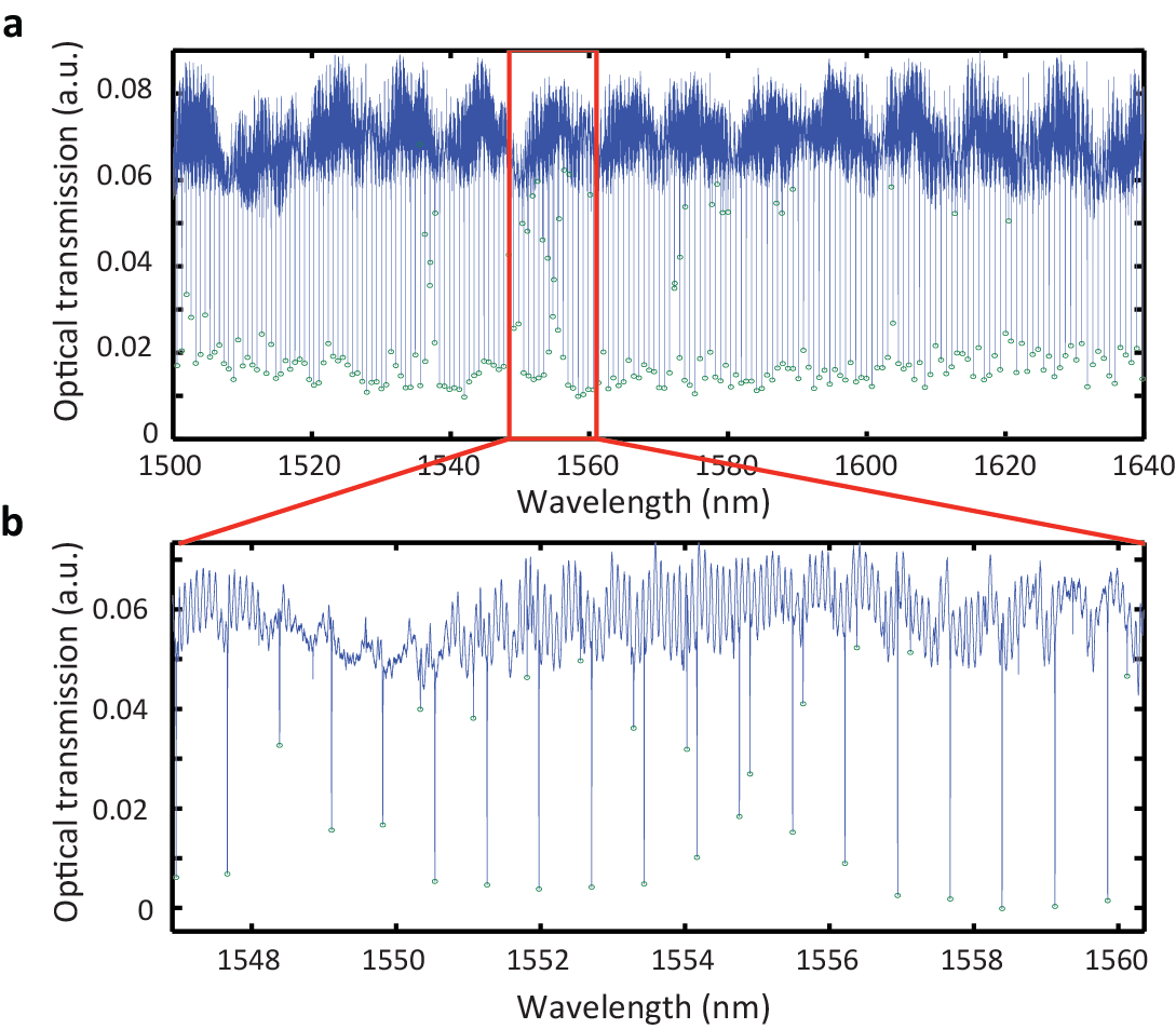
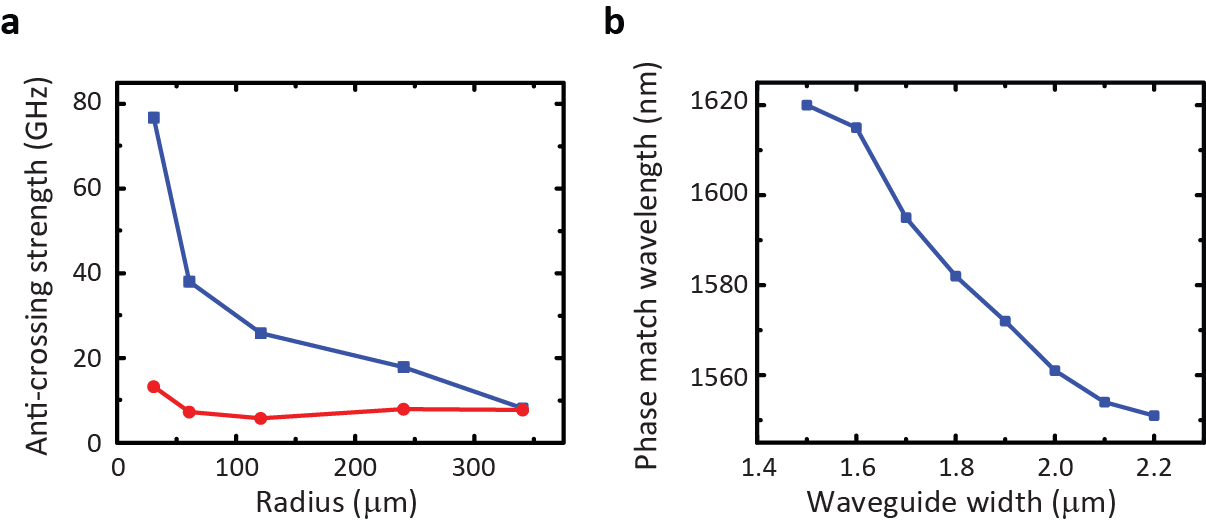
In Fig. S4, we show the measured TE optical spectrum of a AlN ring with radius 240m and width 2.1m. Beside the fundamental TE optical modes, we observe another group of modes around 1555 nm, showing the mixing between TE and TM modes. In addition, the mode extinction ratio also drops, as the coupling rate between the bus waveguide and ring resonator drops. In Fig. S5, we plot the wavelength difference between two adjacent optical resonances. When there is no mixing between TE and TM modes, the wavelength difference corresponds to the free spectral range of the ring resonator. When the mixing happens, the wavelength difference drops below half of the free spectral range, and the smallest wavelength difference gives us the anti-crossing strength between TE and TM modes. Beside the main anti-crossing around 1555 nm, we can also observe anti-crossing around 1538 nm and 1573 nm, corresponding to the azimuthal number different of . As we can see, the anti-crossing strength is much smaller for compared with (Fig. S6a). Here, the mode mixing between the TE and TM modes for is from the surface roughness and the perturbation induced by the external coupling waveguide.
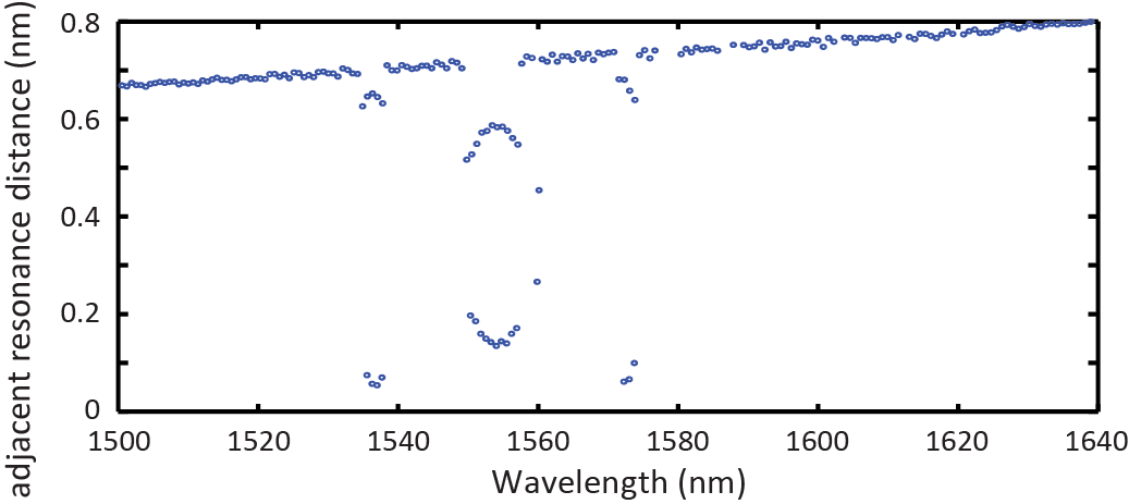
As the vacuum coupling efficiency is inversely proportional to the square root of the ring radius (Eq. (S.3)), we should minimize the ring radius to maximize the vacuum coupling rate. Therefore, instead of using TE and TM modes with the same azimuthal number (), we use the TE and TM modes with azimuthal number different by 1 (), which have a much smaller mode anti-crossing. Accordingly, the microwave azimuthal number should also be designed to be , which will be explained in detail in Sect. III.
With the same ring radius, the phase matching wavelength can be fine-tuned by the waveguide width, which modifies the phase velocity differently for the TE and TM optical modes. Figure S6b shows that the phase matching wavelength can be tuned by 70 nm with a waveguide width change of 600 nm. Therefore we can precisely control the phase matching wavelength to match different wavelength bands, providing the possibility for wavelength domain multiplexing.
IV Influence of optical mode mixing on the vacuum coupling rate
As we can see from the last section, the anti-crossing between TE and TM optical modes sets the lowest possible microwave frequency if triple resonance scheme is used. Furthermore, the vacuum coupling rate is decreased due to the mixing between TE and TM optical modes. The system Hamiltonian for the mode mixing is
| (S.17) |
where is the mode mixing strength between TE and TM optical modes. Since , we first diagonalize the optical part of the Hamiltonian by introducing the hybrid optical modes as
| (S.18) |
where and are the operators for hybrid optical modes, and , satisfying
| (S.19) |
The eigenfrequencies of the hybrid optical modes are
| (S.20) | ||||
| (S.21) |
The minimum frequency difference is therefore , which corresponding to the frequency gap in the anti-crossing spectrum.
By inverting Eq. (S.18), we can obtain
| (S.22) |
Plugging Eq. (S.22) into Eq. (S.2), we obtain the modified electro-optic interaction Hamiltonian
| (S.23) | ||||
| (S.24) |
Comparing with the original interaction Hamiltonian, the modified Hamiltonian has the same form, but lower effective coupling strength .
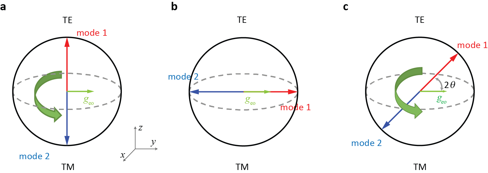
When the detuning between the two original optical modes is zero, thus , the effective electro-optic interaction vanishes. This phenomena can be intuitively shown with the Bloch sphere. Assuming the north and south poles are the TE and TM optical modes respectively, then the electro-optic interaction is equivalent to the rotation along -axis (Fig. S7a). When there is mode anti-crossing and the detune is zero, the two renormalized optical modes involved are maximally hybridized mode, whose directions are along -axis, thus the rotation along -axis will not induce the mode conversion between the two renormalized modes (Fig. S7b). Therefore, the detuning must be non-zero, and the effective vacuum coupling rate is (Fig. S7c). When the detuning is much larger than the anti-crossing strength, the vacuum coupling rate approaches the original value .
V Microwave resonator design
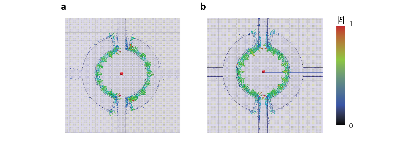
This planar microwave resonator can be treated as two coupled lumped element microwave resonators, where the central disk and surrounding arms provide the dominant capacitance and inductance respectively. The two lumped microwave resonators are coupled through the connection at the central disk. The resonator has symmetric and anti-symmetric modes due to the coupling between capacitors. The simulated electric field distribution is plotted in Fig. S8a and b. The symmetric mode has uniformly distributed electric field with the azimuthal angle , thus the azimuthal number , satisfying the phase matching condition for . And the anti-symmetric mode has a dependence, thus strong component of , satisfying the phase matching condition for .
The lumped element microwave resonator can provide very small electric mode volume, which is critical for enhancing the vacuum coupling rate (Eq. S.3). Also the resonant frequency can be varied by adjusting the arm length of the resonator. Thus the capacitance part of the resonator can be kept fixed, making it easy to match the optical cavity and resonant frequency simultaneously. Another advantage of this design is that the long-arm inductor allows supercurrents to generate magnetic flux far-extended from the chip surface, making it feasible to inductively couple the microwave resonator with an off-chip loop probe for broadband high-efficiency microwave signal input and readout.
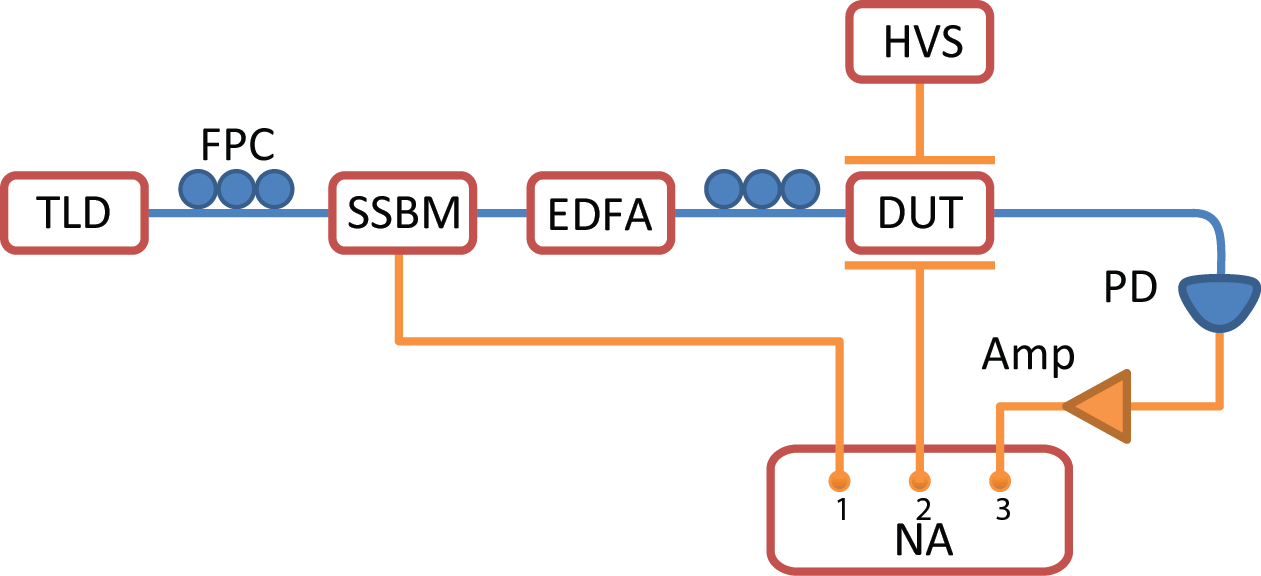
VI Measurement setup
The experiment setup is shown in Fig. S9. Coherent light from a tunable laser diode (TLD) is used as the control light, which is sent into an single side-band modulator (SSBM) to generate a weak probe light. The modulation RF signal is from a network analyzer (NA). Then a erbium doped fiber amplifier (EDFA) is used to amplify the control light. Light is coupled to and from the on-chip bus waveguide through a pair of grating couplers, which only transmit TE light. The output light is detected by the high frequency photodetector (PD). The output signal of the photodetector is amplified by a RF amplifier (Amp), and de-modulated with network analyzer. The microwave port of the device is directly connect to the network analyzer. A high voltage source (HVS) is used to provide the static electric field across the device for optical resonance tuning.
VII Device temperature calibration
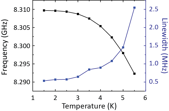
The strong control light can heat up the device, which may degrade the microwave resonator performance. In order to calibrated the device temperature, we measure the microwave resonant frequency and linewidth at different ambient temperatures without light input. As we can see from Fig. S10, the resonator frequency drops and the linewidth increases with the temperature increase. Therefore, by measuring the microwave resonant frequency and linewidth at base temperature with strong control light, we can infer the effective temperature of the microwave cavity. The linewidths at 2.0 K, 2.5 K, and 3.0 K are 0.64 MHz, 0.58 MHz, and 0.54 MHz respectively. As shown in Fig. 2E and Fig.4 E in the main text, the microwave resonance linewidth is around 0.55 MHz under 8 dBm optical pump, indicating that the effective temperature of the device is around 2.1 K.
VIII Efficiency calibration
The cooperativity of is estimated from the fitting of the blue curve in Fig. 3C in the main text, leading to internal efficiency around based on Eq. (S.16). From the resonance extinction ratio , the photon extraction efficiency can be calculated assuming under-coupled condition with for optical signal and microwave modes respectively. From Fig. 2 C & E in the main text, the resonance extinction ratio of optical signal and microwave modes can be extracted, and , leading to extraction efficiency and respectively. Thus the on-chip efficiency can be estimated . We also followed the calibration procedure in Ref. [7]. The complete conversion matrix is measured as shown in Fig. 4 in the main text, including optical reflection , microwave reflection , microwave-to-optical conversion , and optical-to-microwave conversion . The on-resonance conversion efficiency is normalized by the off-resonance reflection amplitude, thus the gain and loss of the measurement circuit are excluded. Assuming that the conversion efficiency is the same for both directions, we estimate on-chip efficiency, which agrees well with the estimation based on the cooperativity and extraction efficiency.
Based on the cooperativity and the resonance linewidth, the enhanced coupling strength can be estimated . The pump photon number inside the pump optical mode is , with the uncertainty determined by the insertion loss (supplementary material of Ref. [34]). Therefore the effective vacuum coupling rate estimated from experimental results is
| (S.25) |
Using finite-element-method simulation with the actual device geometry estimated from Fig. S2, the field distributions (, , ) of the optical pump and signal modes, and the microwave mode can be obtained (Fig. 1D, E, & F). Plugging the field distributions into Eq. (S.4) and assuming [21], the vacuum coupling rate for our device can be calculated as , with the uncertainty determined by the parameter difference between the design and fabricated device estimated from Fig S2. Together with the optical mode mixing strength obtained from Eq. (S.19), the calculated effective vacuum coupling rate is
| (S.26) |
which agrees with our experimental estimation.
IX Added noise during conversion
In addition to the conversion efficiency , the added noise during the conversion process is also an important figure of merit. There are mainly two sources of noise, thermal excitation of the microwave cavity and photons generated by the parametric interaction .
By including the counter-rotating term , we have the
| (S.27) | |||
| (S.28) | |||
| (S.29) | |||
| (S.30) |
Here, and are the noise from the intrinsic loss channels of the optical and microwave cavities respectively. The noise correlators can be expressed as following
| (S.31) | ||||
| (S.32) | ||||
| (S.33) | ||||
| (S.34) |
By solving Eq. (S.27) - (S.30) and the input-output relations Eq. (S.11) & Eq. (S.12), we can obtain the output signal at phase matching condtion
| (S.35) | ||||
| (S.36) |
with the conversion efficiency
| (S.37) | ||||
| (S.38) |
The added noise due to the thermal environment is
| (S.39) | ||||
| (S.40) |
And the noise due the counter-rotating term is
| (S.41) | ||||
| (S.42) |
Compare with Eq. (S.15), the additional term in the conversion efficiency is the counter-rotating term induced amplification. For our experiment parameters with , , and , we estimated the modification of the conversion efficiency due to the parametric amplification factor for the achieved . This indicates that the RWA is valid for our experiments.
For the added noise, we have the thermal excitation for , thus and , which can be further reduced by working at lower temperature. In addition, the noise due to parametric amplification can be estimated, and , which are negligible in our current experiments.